Note: Descriptions are shown in the official language in which they were submitted.
CA 02613719 2011-04-08
THIOPHENE ELECTRONIC DEVICES
CROSS REFERENCE TO RELATED APPLICATIONS
[0001] Illustrated in U.S. Patent No. 7,718,999, filed concurrently
herewith, is an electronic device comprising a semiconductor of the
Formula/Structure (I)
,R
X
i
(C H 2)m
/ \ M
S a b
n
(I)
wherein X is one of 0 or NR'; m represents the number of methylenes; M is a
conjugated moiety; R and R' are selected from the group consisting of at least
one of hydrogen, a suitable hydrocarbon, and a suitable hetero-containing
group; a represents the number of 3-substituted thiophene units; b represents
the number of conjugated moieties, and n represents the number of repeating
units of the polymer.
[0002] U.S. Patent No. 7,834,132, filed October 25, 2006 on Electronic
Devices by Beng S. Ong et al.
[0003] U.S. Patent No. 7,820,782, filed October 25, 2006 on
Poly(dithienylbenzo[1,2-b:4,5-b']dithiophene) Polymers by Beng S. Ong et al.
[0004] U.S. Patent No. 7,372,071, filed April 6, 2006 on Functionalized
Heteroacenes and Electronic Devices Generated Therefrom by Yuning Li et
at.
[0005] U.S. Patent Application Publication No. 2007-0260069, filed
April 6, 2006 on Functionalized Heteroacenes by Yuning Li et at.
-1-
CA 02613719 2011-04-08
[0006] U.S. Patent No. 7,550,760, filed April 6, 2006 on Polyacenes
and Electronic Devices Generated Therefrom by Yuning Li et al.
[0007] U.S. Patent No. 7,557,370, filed April 6, 2006 on Heteroacene
Polymers and Electronic Devices Generated Therefrom by Yuning Li et al.
[0008] U.S. Patent No. 7,586,120, filed April 6, 2006 on Ethynylene
Acene Polymers and Electronic Devices Generated Therefrom by Yuning Li et
al.
[0009] U.S. Patent No. 7,795,373, filed April 6, 2006 on Ethynylene
Acene Polymers by Yuning Li et al.
[0010] U.S. Patent No. 7,449,715, filed April 6, 2006 on
Poly[bis(ethynyl)heteroacenes] and Electronic Devices Generated Therefrom
by Yuning Li et al.
[0011] U.S. Patent No. 7,563,860, filed April 6, 2006 on
Semiconductors and Electronic Devices Generated Therefrom by Yiliang Wu
et al.
[0012] U.S. Patent No. 7,615,607, filed April 6, 2006 on Semiconductor
Polymers by Yiliang Wu et al.
[0013] U.S. Patent No. 7,517,477, filed April 6, 2006 on
Polydiazaacenes and Electronic Devices Generated Therefrom by Yiliang Wu
et al.
[0014] U.S. Patent No. 7,517,476, filed April 6, 2006 on
Polydiazaacenes by Yiliang Wu et al.
[0015] U.S. Patent Application Publication No. 2007-0235719, filed
April 6, 2006 on Poly(alkynylthiophene)s and Electronic Devices Generated
Therefrom by Beng S. Ong et al.
[0016] U.S. Patent No. 7,705,111, filed April 6, 2006 on
Poly(alkynylthiophene)s by Beng S. Ong et al.
-2-
CA 02613719 2011-04-08
[0017] U.S. Patent No. 7,619,055, filed April 6, 2006 on Linked
Arylamine Polymers and Electronic Devices Generated Therefrom by Yuning
Li et al.
[0018] U.S. Patent No. 7,847,052, filed April 6, 2006 on Linked
Arylamine Polymers by Yuning Li et al.
[0019] U.S. Patent Application Publication No. 2006-0124921, filed
December 14, 2004, relating to indolocarbazole moieties and thin film
transistor devices thereof.
[0020] U.S. Patent No. 7,402,681, Publication No. 20060214155, filed
June 27, 2005, relating to indolocarbazole moieties and thin film transistor
devices thereof.
[0021] Illustrated in U.S. Patent 6,770,904 and U.S. Patent No.
7,250,625, Publication No. 20050017311 are electronic devices, such as thin
film transistors containing semiconductor layers of, for example,
polythiophenes.
[0022] In aspects of the present disclosure, there may be selected the
appropriate substituents, such as a suitable hydrocarbon, a heteroatom
containing group, hydrogen, halogen, source and gate electrodes, substrates,
number of repeating polymer units, number of groups, and the like as
illustrated in the copending applications.
BACKGROUND
[0023] The present disclosure is generally directed to semiconductors
of the formulas/structures as illustrated herein, and processes of preparation
and uses thereof. More specifically, the present disclosure in embodiments
is directed to novel classes of substituted aromatic vinyl-based thiophene
semiconductors of the formulas as illustrated herein which are believed to
be more stable than, for example, acene-based semiconducting materials.
These semiconducting materials can be dissolved or blended in a polymer
binder for fabricating uniform thin films which can be selected
as semiconductors for TFTs. Accordingly, in
-3-
CA 02613719 2007-12-07
embodiments it is believed that the dissolved semiconductor molecules can
crystallize out and form a continuous highly ordered semiconducting film to
provide excellent TFT performance characteristics, such as efficient field
effect
charge carrier transport. In embodiments, the new semiconducting materials can
be selected as semiconductors for thin-film transistors, and also which can be
selected as solution processable and substantially stable channel
semiconductors
in organic electronic devices, such as thin film transistors, and which
devices can
be generated by economical solution processes, and which electronic devices
are
stable in air, that is do not substantially degrade over a period of time when
exposed to oxygen.
[0024] There are desired electronic devices, such as thin film transistors,
TFTs, fabricated with a semiconductor of the formulas as illustrated herein,
and
which semiconductors possess excellent solvent solubility, and which can be
solution processable; and wherein these devices possess mechanical durability
and structural flexibility characteristics which are desirable for fabricating
flexible
TFTs on a number of substrates, such as plastic substrates. Flexible TFTs
enable
the design of electronic devices with structural flexibility and mechanical
durability
characteristics. The use of plastic substrates together with the semiconductor
of
the formulas as illustrated herein can transform the traditionally rigid
silicon TFT
into a mechanically more durable and structurally flexible TFT design. This
can
be of particular value to large area devices such as large area image sensors,
electronic paper, and other display media. Also, the selection of the
semiconductors of the formulas as illustrated herein possess in embodiments
extended conjugation for integrated circuit logic elements for low end
microelectronics, such as smart cards, radio frequency identification (RFID)
tags,
and memory/storage devices, and enhance their mechanical durability, and thus
their useful life span.
[0025] A number of semiconductor materials are not, it is believed, stable
when exposed to air as they become oxidatively doped by ambient oxygen
resulting in increased conductivity. The result is large off current and thus
a low
current on/off ratio for the devices fabricated from these materials.
Accordingly,
-4-
CA 02613719 2007-12-07
with many of these materials, rigorous precautions are usually undertaken
during
materials processing and device fabrication to exclude environmental oxygen to
avoid or minimize oxidative doping. These precautionary measures increase the
cost of manufacturing therefore offsetting the appeal of certain semiconductor
TFTs as an economical alternative to amorphous silicon technology,
particularly
for large area devices. These and other disadvantages are avoided or minimized
in embodiments of the present disclosure.
REFERENCES
[0026] Regioregular polyhexylthiophenes usually undergo rapid photo
oxidative degradation under ambient conditions, while the know
polytriarylamines
possess some stability when exposed to air, however, these amines are believed
to possess low field effect mobilities, disadvantages avoided or minimized
with the
polymers of the formulas as illustrated herein.
[0027] Also, acenes, such as pentacene and heteroacenes, are known to
possess acceptable high field effect mobility when used as channel
semiconductors in TFTs. However, these materials can be rapidly oxidized by,
for
example, atmospheric oxygen under light, and such compounds are not
considered processable at ambient conditions. Furthermore, when selected for
TFTs, acenes have poor thin film formation characteristics and are
substantially
insoluble, thus they are essentially nonsolution processable; accordingly,
such
compounds have been processed by vacuum deposition methods that result in
high production costs, eliminated or minimized with the TFTs generated with
the
semiconductors illustrated herein.
[0028] A number of organic semiconductor materials has been described
for use in field effect TFTs, which materials include organic small molecules,
such
as pentacene, see for example D.J. Gundlach et at., "Pentacene organic thin
film
transistors - molecular ordering and mobility", IEEE Electron Device Lett.,
Vol. 18,
p. 87 (1997); oligomers such as sexithiophenes or their variants, see for
example
reference F. Garnier et at., "Molecular engineering of organic semiconductors:
Design of self-assembly properties in conjugated thiophene oligomers", J.
Amer.
-5-
CA 02613719 2007-12-07
Chem. Soc., Vol. 115, p. 8716 (1993), and poly(3-alkylthiophene), see for
example reference Z. Bao et al., "Soluble and processable regioregular poly(3-
hexyithiophene) for field-effect thin film transistor application with high
mobility',
App!. Phys. Lett. Vol. 69, p4108 (1996). Although organic material based TFTs
generally provide lower performance characteristics than their conventional
silicon
counterparts, such as silicon crystal or polysilicon TFTs, they are
nonetheless
sufficiently useful for applications in areas where high mobility is not
required.
These include large area devices, such as image sensors, active matrix liquid
crystal displays and low end microelectronics such as smart cards and RFID
tags.
[0029] TFTs fabricated from p-type semiconductor polymers of the formulas
illustrated herein may be functionally and structurally more desirable than
conventional silicons and other semiconductors in that they may offer
mechanical
durability, structural flexibility, and the potential of being able to be
incorporated
directly onto the active media of the devices, thus enhancing device
compactness
for transportability. Also, a number of known small molecule or oligomer-based
TFT devices rely on difficult vacuum deposition techniques for fabrication.
Vacuum deposition is selected primarily because the materials selected are
either
insoluble or their solution processing by spin coating, solution casting, or
stamp
printing does not generally provide uniform thin films.
[0030] Further, vacuum deposition may also involve the difficulty of
achieving consistent thin film quality for large area format. Polymer TFTs,
such as
those fabricated from regioregular components of, for example, regioregular
poly(3-alkylthiophene-2,5-diyl) by solution processes, while offering some
mobility,
suffer from their propensity towards oxidative doping in air. For practical
low cost
TFT design, it is therefore of value to have a semiconductor material that is
both
stable and solution processable, and where its performance is not adversely
affected by ambient oxygen, for example, TFTs generated with poly(3-
alkylthiophene-2,5-diyl) are sensitive to air. The TFTs fabricated from these
materials in ambient conditions generally exhibit large off-current, very low
current
on/off ratios, and their performance characteristics degrade rapidly.
-6-
CA 02613719 2011-04-08
[0031] Additional references that may be of interest include U.S. Patent
Nos. 6,150,191; 6,107,117; 5,969,376; 5,619,357, 5,777,070 and 6,774,393.
SUMMARY OF INVENTION
[0031 a] In accordance with another aspect, there is provided an electronic
device comprising a semiconductor, wherein said semiconductor comprises a
compound selected from Formulas (2), (3), and (5) to (15):
Rn
Rm S
I C i -Ar
S
Ar C-C R'
\ S Rm
R' Y x
Rn
(2)
Rn
Rm S
R' C-~-Ar
C C
Y S Rm _ R
I I
x
Rn
(3)
Rn Rn
R
I ' _ _ R'
S
C=C-Ar
Y y R'
S
Rm Rm x
(5)
-7-
CA 02613719 2011-04-08
Rn
S Rm
I
s S
y
~k ,,, S z s \ y C-Ar
R m x R'
Rn
(6)
Rn
R'
S S Rm
Ar-C- I R'
R S S \ / y -C Ar
z x
Rm R
Rn
(7)
Rm Rn
R S S R
C- i -Ar
Ar-C - ky s
S z y
Rn x
Rm
(8)
-7a-
CA 02613719 2011-04-08
Rn
Rm
R' s s R'
11 Ar-C-C \ / \ / \ / \ C-C-Ar
Y y R
x Rn
Rm
(9)
Rm Rn
s S \ R'
S C-~-Ar
Ar-C~~ g Y
y S
R
Rn Rm x
(10)
Rm Rn
s S R'
R' I
I C- i -Ar
Ar C C G\-// y
S S y
z
R'
Rim x
Rn
(11)
Rn Rm
R' s R'
Ar-C-C / \ \ -Ar
Ys C\,Xu- z x Rn
Rm
(12)
-7b-
CA 02613719 2011-04-08
Rn Rm
S I\ S R
Ar-C O\/ C-~-Ar
R (O)
S Y R
Y
z x I
Rn
Rm
(13)
Rm Rn
s / \ s / \ ELAr
ArC=C I / S S Y
Y x R
Rn Rm
(14)
Rn Rm
R' S i '
Ar =C FC-Ar
R' Y x v R'
Rn
Rm
(15)
wherein R' is independently selected from hydrogen, alkyl, substituted alkyl,
alkoxy, substituted alkoxy, aryl, and substituted aryl; R is selected from
alkyl,
substituted alkyl, alkoxy, substituted alkoxy, aryl, and substituted aryl,
halogen,,
and hydrogen; m and n represent the number of substituents; Ar is aryl; and x,
y,
and z represent the number of repeating units.
-7c-
CA 02613719 2011-04-08
[0031 b] In accordance with a further aspect, there is provided an electronic
device comprising a semiconductor, wherein the semiconductor comprises a
compound selected from Formulas (a) through (q):
a\\ R" R"
S \ /
(a)
R
S
R" I R"
S
R
(b)
S
Rõ 1:S
(c)
R
S S
- S \ S
R
(d)
-7d-
CA 02613719 2011-04-08
R
S
R"
(e)
R"
(9)
R"
S S
R"
S g
R"
(h)
-7e-
CA 02613719 2011-04-08
R-
s S
R- / \ \ I \ \ / R..
S S
\i)
\ S \ ~
U)
/ \ S
Rõ
R'
/ \ --O -R"
S
R,...
(k)
R"
S
(I)
-7f-
CA 02613719 2011-04-08
R
R
\ / \ S
R..
R -C -O -R"
S
R
R....
(m)
R
R / S \ / R..
S
R"'
(n)
R
R
s
(0)
R R
Rõ / \ = S
S i S
R... R"
(p)
-7g-
CA 02613719 2011-04-08
R' S
(q)
wherein R", R"', and R"" are independently selected from alkyl having from 1
to
about 35 carbon atoms, substituted alkyl having from 1 to 35 carbon atoms,
perfluoroalkyl having from 1 to 12 carbon atoms, alkoxy having from 1 to 18
carbon atoms, and alkoxy having from 1 to 18 carbon atoms.
[0031 c] In accordance with another aspect, there is provided an electronic
device comprising a semiconductor, wherein said semiconductor comprises a
compound of Formula (4):
R' Rn Rn
I S S I R'
I
Ar-C-C C-C-Ar
S Y S Y
R
S z
Rm Rm x
(4)
wherein R' is independently selected from hydrogen, alkyl, substituted alkyl,
alkoxy, substituted alkoxy, aryl, and substituted aryl; R is selected from
alkyl,
substituted alkyl, alkoxy, substituted alkoxy, aryl, and substituted aryl,
halogen,
and hydrogen; m and n represent the number of substituents; where m is 0 or 1,
and n is 0, 1, or 2; Ar is aryl; and x, y, and z represent the number of
repeating
units, where x is a number from 1 to 6, y is a number from 0 to 4, and z is a
number from 1 to 3.
[0031d] In accordance with a further aspect, there is provided a
semiconductor comprised of:
-7h-
CA 02613719 2011-04-08
Rn
Rm S
i1
R' C-C-Ar
S
R'
Ar C= i I
S Rm
R Y x
Rn
(2)
Rn
Rm S
Ar C=C / \ / \ Y R'
S Rm
y X
Rn
(3)
Rn
R s Rm
Ar- i =C \ / \ / -
4/ S\ S
Y S z s \ S / y -C-Ar
Rm x R'
Rn
(6)
-7i-
CA 02613719 2011-04-08
Rn
S S Rm
Ar C - I / I \ R'
I I
R ~:::--C-Ar
s s x\ / y
Rm R'
Rn
(7)
Rm Rn
S
Ar-CC
- -~/ S Y
\ yy
R' S z
Rn x
Rm
(8)
Rn
Rm
R' S S R'
~ :/ I
Ar-C=C / \
R' Y S z I Y R'
x Rn
Rm
(9)
Rm Rn
s S R'
R' s
Ar C - S }
Y S S z
R'
Rm x
Rn
(10)
-7j-
CA 02613719 2011-04-08
Rm Rn
S S R'
Ar-C
S S z Y
R'
Rm X
Rn
(11)
wherein R' is independently at least one of hydrogen, alkyl, alkoxy, and aryl;
R is
at least one of alkyl, alkoxy, aryl, a halogen, and hydrogen; m and n
represent
the number of substituents; Ar is selected from the group consisting of
phenyl,
alkylphenyl, halophenyl and alkoxyphenyl; x, y, and z represent the number of
repeating units, wherein x is from 1 to 6, y is from 0 to 4 and z is from 0 to
3
BRIEF DESCRIPTION OF THE DRAWINGS
[0032] Illustrated in Figures 1 to 4 are various representative
embodiments of the present disclosure, and wherein semiconductors of the
formulas as illustrated herein are selected as the channel or semiconductor
material in thin film transistor (TFT) configurations.
DESCRIPTION OF THE EXEMPLARY EMBODIMENTS
[0033] It is a feature of the present disclosure to provide semiconductors
of the formulas as illustrated herein, which are useful for microelectronic
device
applications, such as TFT devices.
[0034] It is another feature of the present disclosure to provide
semiconductors of the formulas as illustrated herein with a band gap of from
about 1.5 eV to about 4 eV (electron volts) as determined from the absorption
spectra of thin films thereof.
[0035] In yet a further feature of the present disclosure there are
provided p-type semiconductors of the formulas illustrated herein which are
-7k-
CA 02613719 2011-04-08
useful as microelectronic components, and which semiconductors possess a
solubility of, for example, at least about 0.1 percent to about 95 percent by
weight in common organic solvents, such as methylene chloride,
tetrahydrofuran, toluene, xylene, mesitylene, chlorobenzene, dichlorobenzene,
trichlorobenzene and the like, and thus these semiconductors can be
economically fabricated by solution processes such as spin coating, screen
printing, stamp printing, dip coating, solution casting, jet printing, and the
like.
[0036] Another feature of the present disclosure provides p-type
semiconductors of the formulas as illustrated herein which can be dissolved or
blended in a polymer binder resin for fabricating uniform thin films which can
be
selected as semiconductors for TFTs. Thus, in embodiments it is believed that
-71-
CA 02613719 2007-12-07
the dissolved semiconductor molecules can crystallize out and form a
continuous
highly ordered semiconducting film to provide excellent TFT performance
characteristics, such as efficient field effect charge carrier transport.
[0037] A process for the preparation of the semiconductor involves
generating a dispersion or a solution comprised of (a) a continuous phase
comprising a solvent, a binder resin, and an optional dispersing agent, and
(b) a
dispersed phase or a solution comprising the organic semiconductor material of
the formulas illustrated herein. In embodiments the degree of solubility of
the
semiconductor material in the solvent may vary in embodiments of, for example,
from 0 percent to about 100 percent solubility, and more specifically from 0.5
percent to about 100 percent solubility.
[0038] The binder resin and the optional dispersing agent in embodiments
are substantially soluble in the solvent, inclusive of being completely
dissolved in
the solvent. However, the degree of solubility of the binder resin and the
dispersing agent in the solvent may vary in embodiments from, for example,
about
95 percent to 100 percent solubility by weight, and more specifically from
about 99
percent to 100 percent solubility by weight.
[0039] In the dispersion (or the solution) and the semiconductor layer, the
components can be present in various concentrations. For example, the
semiconductor material is present in an amount of, for example, from about 20
percent to about 99.5 percent by weight, and more specifically, from about 60
percent to about 95 percent by weight, based on the total weight of the
semiconductor material and the binder resin. The binder resin is present in an
amount of, for example, from about 80 percent to less than about 1 percent by
weight, and more specifically, from about 40 percent to about 5 percent by
weight,
based on the total weight of the semiconductor material and the binder resin.
The
ratio of optional dispersing agent to binder resin is, for example, from 0 to
about
0.5 by weight, while the solvent is present in an amount of, for example, from
about 10 percent to about 95 percent, and more specifically, from about 50
percent by weight to about 90 percent by weight, based on the total weight of
the
dispersion or the solution.
-8-
CA 02613719 2011-04-08
[0040] The binder resin functions primarily as a medium for the organic
semiconductor materials to permit the semiconductor layer to be fabricated by
a
solution process, such as spin coating, dip coating, solution casting, stamp
printing, or jet printing, and the like, to thereby form a uniform
semiconductor
layer. The binder resin, which is electrically insulating or semiconducting,
may be
selected for instance from a number of known oligomers and polymers as
illustrated herein, and more specifically, poly(vinyl butyral), polyesters,
polycarbonates, poly(vinyl chloride), polyacrylates and methacrylates,
copolymers
of vinyl chloride and vinyl acetate, phenoxy resins, polyurethanes, poly(vinyl
alcohol), polyacrylonitrile, polystyrene, semiconductor polymers, such as
polythiophenes, mixtures thereof and the like. Subsequent to the solvent
evaporation from the coated dispersion or the coating solution, the binder
resin
usually forms a substantially smooth, continuous phase that adheres to the
substrate and uniformly coats the semiconductor material. In embodiments, the
binder resin may also function as a dispersant for the particles of the
semiconductor material by minimizing agglomeration, increasing the dispersion
uniformity, and preventing settling of the semiconductor material when the
dispersion is stored.
[0041] A dispersing agent can be included in the semiconductor layer
dispersion in an amount of, for example, from about 0.1 percent to about 50
percent, and more specifically, from about 1 percent to about 10 percent of
the
weight of the binder resin. Many types of dispersing agents are known (as
described, for example, in the book "McCutcheon's, Volume 1: Emulsifiers and
Detergents", published annually by McCutcheon's division, MC Publishing Co.,
175 Rock Road, Glen Rock, N.J., 07452), including those dispersants
illustrated
herein such as ethoxylated long-chain alcohols, glyceryl stearates,
alkanolamides,
sodium lauryl sulfate, alkylnaphthalene sulfonates, and aliphatic-based
phosphate
esters; trimethyl cetyl ammonium chloride, oleic imidazoline and ethoxylated
fatty
amines, lecithin and polyglycol ether derivatives, and which agent primarily
functions to stabilize the dispersed semiconductor material against
flocculation,
-9-
CA 02613719 2007-12-07
aggregation or sedimentation, and thereby maintains the dispersion in a finely
divided state.
[0042] Another feature of the present disclosure resides in providing
electronic devices, such as TFTs, with p-type semiconductors of the formulas
as
illustrated herein for organic thin film transistors, and which semiconductor
layer
has a conductivity of, for example, from about 10"4 to about 10"10 S/cm
(Siemens/centimeter).
[0043] Also, in yet another feature of the present disclosure there are
provided novel p-type semiconductors of the formulas as illustrated herein and
devices thereof, and which devices exhibit enhanced resistance to the adverse
effects of oxygen, that is, these devices exhibit relatively high current
on/off ratios,
and their performance does not substantially degrade as rapidly as similar
devices
fabricated with acenes or with regioregular poly(3-alkylthiophene-3,5-diyl).
[0044] Additionally, in a further feature of the present disclosure there is
provided a class of novel p-type semiconductors of the formulas as illustrated
herein with unique structural features which are conducive to molecular self-
alignment under appropriate processing conditions, and which structural
features
also enhance the stability of device performance. Proper molecular alignment
can
permit higher molecular structural order in thin films, which can be of value
to
efficient charge carrier transport, and thus higher electrical performance.
[0045] There are disclosed in embodiments semiconductors of the formulas
as illustrated herein and electronic devices thereof. More specifically, the
present
disclosure relates to semiconductor materials illustrated by or encompassed by
Formula/Structure (I)
R' R'
I I
Ar-C= C- M-C= C-Ar
(I)
wherein each R' is independently hydrogen, a suitable hydrocarbon, such as
alkyl,
alkoxy, haloalkyl, aryl, substituted derivatives thereof, and the like; Ar is
an aryl or
heteroaryl substituent with, for example, from 6 to about 42 carbon atoms,
such as
-10-
CA 02613719 2007-12-07
phenyl, alkylphenyl, halophenyl like chiorophenyl, alkoxyphenyl, and the like;
and
M represents at least one thiophene based conjugated segment.
[0046] Examples of semiconductor components or materials (I) include, but
are not limited to, those substituted aromatic vinyl-based thiophene
semiconductors of the following formulas/structures
Rm
Fr R'
Ar-C-C C=C-Ar
I S X
R R'
(1)
-11-
CA 02613719 2007-12-07
Rn
s S
R
C-C-Ar
I \
/ / s Y
Ar C - C I
K'
S Rm
y x
R' I
Rn
(2)
Rn
Rm S
C-C-Ar
I,
S Rm
R' Y x
Rn
(3)
Rn Rn
Ar-C=C -K : C-C-Ar
Rs / S Y
R
S z
Rm Rm x
(4)
-12-
CA 02613719 2007-12-07
Rn Rn
R' _ _ R'
I S S I
Ar-i-C \ i =C-Ar
R' Y I Y R'
S
Rm Rm x
(5)
Rn
R'
I S S Rm
S
-C-Ar
R' Y k-s z s i
Rm x I R'
Rn
(6)
Rn
R=
S S RIm
Ar=C- I / I \ ` R'
I - Y I -
R S z x y ~Ar
Rm I R'
Rn
(7)
Rm Rn
I' S S S R'
C= i -Ar
R' S z S Y R'
Rn Rm x
(8)
-13-
CA 02613719 2007-12-07
Rn
Rm
S R'
Ar-C-C I -
Y S z I Y I
R'
Rm x Rn
(9)
Rm Rn
R S S I \
R i,
\` I Y S S Z R'
Rn Rm x
(10)
Rm Rn
s S R'
C-C-Ar
Ar-C=C,
a,-/ S S Z Y R
R
Rm x
Rn
(11)
Rn Rm
R' S R'
Ar-C= i / I \ \ \ 1 = -
R' Y S I Y R'
z x Rn
Rm
(12)
Rn Rm
R' / I \ S ~ ~ I\ g I
Ar-C \ C-C-Ar
s y S \ I/ ~Y-
R' z I R'
Rm x Rn
-14-
CA 02613719 2007-12-07
(13)
Rm Rn
R R'
Ar-C-i S =I-Ar
R X R'
I I** S Y
Rn Rm
(14)
Rn Rm
R' R'
Ar-~~C S FG-Ar
R' Y Y R'
Rn
Rm
(15)
wherein R' and Ar are as illustrated herein with respect to Formula (I); R
represents suitable substituents on the aromatic and thiophene rings,
respectively,
and more specifically, R is a suitable hydrocarbon like alkyl, aryl, alkoxy,
and
substituted derivatives thereof; a halogen; hydrogen, and the like; m and n
represent the number of substituents, and in embodiments are zero (0), 1, 2,
3, or
4; and x, y, and z represent the number of repeating units, or segments, for
example, x can be a number of 1, 2, 3, 4, 5, or 6; y can be zero (0), 1, 2, 3,
or 4;
and z can be zero (0), 1, 2, and 3.
[0047] Alkyl includes, for example, those substituents with from about 1 to
about 35 carbon atoms of, for example, methyl, ethyl, propyl, butyl, pentyl,
hexyl,
heptyl, octyl, nonyl, decyl, undecyl, dodecyl, tridecyl, tetradecyl,
pentadecyl,
hexadecyl, heptadecyl, octadecyl, nonadecyl, eicosanyl, trifluoromethyl,
-15-
CA 02613719 2007-12-07
perfluoroethyl perfluoropropyl, perfluorobutyl, perfluoropentyl,
perfluorohexyl,
perfluoroheptyl, perfluorooctyl, perfluorononyl, perfluorodecyl,
perfluoroundecyl, or
perfluorododecyl. Alkoxy includes, for example, those substituents with from
about 1 to about 35 carbon atoms of, for example, methoxy, ethoxy, propoxy,
butoxy, pentyloxy, hexyloxy, heptyloxy, octyloxy, nonyloxy, decyloxy,
undecyloxy,
dodecyloxy, tridecyloxy, tetradecyloxy, pentadecyloxy, hexadecyloxy,
heptadecyloxy or octadecyloxy. Aryl examples are those groups with, for
example, from about 6 to about 42 carbon atoms of, for example, phenyl,
naphthyl, methylphenyl (tolyl), ethylphenyl, propylphenyl, butylphenyl,
pentylphenyl, hexylphenyl, heptylphenyl, octylphenyl, nonylphenyl,
decylphenyl,
undecylphenyl, dodecylphenyl, tridecylphenyl, tetradecylphenyl,
pentadecylphenyl, hexadecylphenyl, heptadecylphenyl, octadecylphenyl,
halophenyls like chlorophenyl, alkoxyphenyls, and the like.
[0048] Specific examples of the thiophene semiconductors are
s
R" R"
S
(a)
R"'
s
Re / \ I \ R
S
R,..
(b)
-16-
CA 02613719 2007-12-07
S
S \ S \ / \
(C)
R,,,
S S
S S
R
(d)
R
S
Rõ / \ I \ \ Rõ
S
R"
(e)
S R",
-17-
CA 02613719 2007-12-07
\ \ / R"
(g)
R"
s s
R" R"
S 9
R"
(h)
R"'
S S
S S
(i)
~, / \ S \ \ Rõ
s
G)
R
R
-18-
CA 02613719 2007-12-07
(k)
R"
R=
S
RP"
(I)
Fr"
S
R
(m)
R
(n)
R"
R,. / \ S / I \ S
(0)
-19-
CA 02613719 2007-12-07
RR,,
8 S \ / R
R" R
(P)
\ I Rõ
(4)
-20-
CA 02613719 2007-12-07
(r)
S
R111 R"
(s)
R,,,
S S
R"=
(t)
wherein R", R"', and R"" independently represent at least one of alkyl, or
substituted alkyl groups with from about 1 to about 35 carbon atoms of, for
example, but not limited to, an alkyl or substituted alkyl of methyl, ethyl,
propyl,
butyl, pentyl, hexyl, heptyl, octyl, nonyl, decyl, undecyl, dodecyl, tridecyl,
tetradecyl, pentadecyl, hexadecyl, heptadecyl, octadecyl, nonadecyl,
elcosanyl,
trifluoromethyl, perfluoroethyl perfluoropropyl, perfluorobutyl,
perfluoropentyl,
perfluorohexyl, perfluoroheptyl, perfluorooctyl, perfluorononyl,
perfluorodecyl,
perfluoroundecyl, or periluorododecyl, methoxy, ethoxy, propoxy, butoxy,
pentyloxy, hexyloxy, heptyloxy, octyloxy, nonyloxy, decyloxy, undecyloxy,
dodecyloxy, tridecyloxy, tetradecyloxy, pentadecyloxy, hexadecyloxy,
heptadecyloxy or octadecyloxy, and substituted derivatives thereof, and the
like.
-21-
CA 02613719 2007-12-07
[0049] The semiconductor materials can be prepared by a number of
suitable methods, such as, for example, the processes as illustrated with
reference to the following reaction Scheme 1
SCHEMEI
R' ,0
Ar-C=C-B. + Br M Br
R' 0
Pd(PPh3)4
Na2CO3
toluene
90-950C
R' R'
Ar C C M C C Ar
1
R' R'
wherein R', Ar and M are as illustrated herein with respect to structure (I).
[0050] The semiconductors of the formulas/structures illustrated herein are
believed to be soluble or substantially soluble in common coating solvents,
for
example, in embodiments they possess a solubility of at least about 0.1
percent
by weight, and more specifically, from about 0.1 percent to about 10 percent,
or to
about 95 percent by weight in such solvents as methylene chloride, 1,2-
dichloroethane, tetrahydrofuran, toluene, xylene, mesitylene, chlorobenzene,
dichlorobenzene, and the like. Moreover, p-type semiconductors of the formulas
as illustrated herein provide a stable conductivity of, for example, from
about 10-9
S/cm to about 10-4S/cm, and more specifically, from about 10$ S/cm to about 10-
5
S/cm as determined by conventional four-probe conductivity measurements.
[0051] It is believed that the semiconductors of the formulas disclosed
when fabricated from solutions as thin films of, for example, from about 10
nanometers to about 500 nanometers, or from about 50 to about 300 nanometers
in thickness materials are more stable in ambient conditions than similar
devices
-22-
CA 02613719 2007-12-07
fabricated from acene-based semiconducting materials or poly(3-alkylthiophene-
2,5-diyl). When unprotected, the aforementioned p-type semiconductors of the
formulas as illustrated herein and devices thereof are generally stable for a
number of weeks, months rather than days, or hours as is the situation with
from
acene-based semiconducting materials or poly(3-alkylthiophene-2,5-diyl) after
exposure to ambient oxygen, thus the devices fabricated from the
semiconductors
of the formulas as illustrated herein can provide higher current on/off
ratios, and
their performance characteristics do not substantially change as rapidly as
acene-
based semiconducting materials or poly(3-alkylthiophene-2,5-diyl) when no
rigorous procedural precautions have been taken to exclude ambient oxygen
during material preparation, device fabrication, and evaluation.
[0052] In further aspects of the present disclosure there is provided a thin
film transistor comprised of a substrate, a gate electrode, a gate dielectric
layer, a
source electrode and a drain electrode, and in contact with the source/drain
electrodes and the gate dielectric layer a semiconductor layer comprised of
the
semiconducting materials of formulas/structures illustrated herein; an
electronic
device comprising a semiconductive component, and wherein the device is a thin
film transistor, and the component is selected from the group consisting of at
least
one of the formulas/structures (1) to (15) illustrated herein; a TFT device
wherein
the substrate is a plastic sheet of a polyester, a polycarbonate, or a
polyimide; the
gate source and drain electrodes are each independently comprised of gold,
nickel, aluminum, platinum, indium titanium oxide, or a conductive polymer,
and
the gate dielectric is a dielectric layer comprised of silicon nitride or
silicon oxide; a
TFT device wherein the substrate is glass or a plastic sheet; the gate, source
and
drain electrodes are each comprised of gold, and the gate dielectric layer is
comprised of the organic polymer poly(methacrylate), or poly(vinyl phenol); a
device wherein the semiconductor layer is formed by solution processes of spin
coating, stamp printing, screen printing, or jet printing; a device wherein
the gate,
source and drain electrodes, the gate dielectric, and semiconductor layers are
formed by solution processes of spin coating, solution casting, stamp
printing,
screen printing, or jet printing; and a TFT device wherein the substrate is a
plastic
-23-
CA 02613719 2007-12-07
sheet of a polyester, a polycarbonate, or a polyimide, and the gate, source
and
drain electrodes are fabricated from the organic conductive polymer
polystyrene
sulfonate-doped poly(3,4-ethylene dioxythiophene), or from a conductive
ink/paste
compound of a colloidal dispersion of silver in a polymer binder, and the gate
dielectric layer is organic polymer or inorganic oxide particle-polymer
composite;
and thin film transistors thereof.
DESCRIPTION OF THE FIGURES
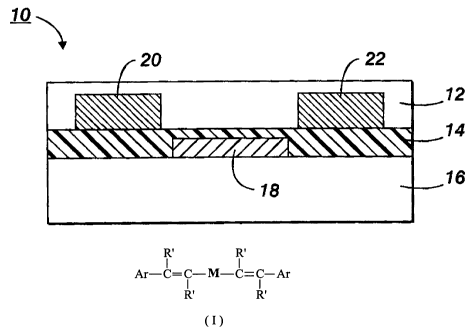
[0053] In Figure 1 there is schematically illustrated a TFT configuration 10
comprised of a substrate 16, in contact therewith a metal contact 18 (gate
electrode), and a layer of an insulating dielectric layer 14 with the gate
electrode
having a portion thereof or the entire gate in contact with the dielectric
layer 14 on
top of which layer 14 two metal contacts, 20 and 22 (source and drain
electrodes),
are deposited. Over and situated between the metal contacts 20 and 22 is layer
12 comprised of the thiophene semiconductors encompassed by
Formula/Structure (I), and more specifically, 2,5-bis[2-(4-pentylphenyl)vinyl]-
thieno(3,2-b)thiophene, structure (a) where R represents pentyl.
[0054] The gate electrode can be included in the substrate, in the dielectric
layer, and the like throughout.
[0055] Figure 2 schematically illustrates another TFT configuration 30
comprised of a substrate 36, a gate electrode 38, a source electrode 40, and a
drain electrode 42, an insulating dielectric layer 34, and the semiconductor
layer
32 of 2,5-bis[2-(4-pentylphenyl)vinyl]-thieno(3,2-b)thiophene, structure (a)
where
R represents pentyl.
[0056] Figure 3 schematically illustrates a further TFT configuration 50
comprised of a heavily n-doped silicon wafer 56, which can act as a gate
electrode, a thermally grown silicon oxide dielectric layer 54, the thiophene
semiconductor layer 52 of 2,5-bis[2-(4-pentylphenyl)vinyl]-thieno(3,2-
b)thiophene,
in example structure (a) where R represents pentyl, on top of which are
deposited
a source electrode 60 and a drain electrode 62; and a gate electrode contact
64.
-24-
CA 02613719 2007-12-07
[0057] Figure 4 schematically illustrates a TFT configuration 70 comprised
of substrate 76, a gate electrode 78, a source electrode 80, a drain electrode
82,
the p-type semiconductor 2,5-bis[2-(4-pentylphenyl)vinyl]-thieno(3,2-
b)thiophene,
layer 72, and an insulating dielectric layer 74.
[0058] Also, other devices not disclosed, especially TFT devices, are
envisioned, reference, for example, known TFT devices. For example, an
optional
protecting layer may be incorporated on top of each of the transistor
configurations of Figures 1, 2, 3 and 4. For the TFT configuration of Figure
4, the
insulating dielectric layer 74 may also function as a protecting layer.
[0059] In embodiments, and with further reference to the present disclosure
and the Figures, the substrate layer may generally be a silicon material
inclusive
of various appropriate forms of silicon, a glass plate, a plastic film or a
sheet, and
the like depending on the intended applications. For structurally flexible
devices,
a plastic substrate, such as for example polyester, polycarbonate, polyimide
sheets, and the like, may be selected. The thickness of the substrate may be,
for
example, from about 10 micrometers to over 10 millimeters with a specific
thickness being from about 50 to about 100 micrometers, especially for a
flexible
plastic substrate, and from about 1 to about 10 millimeters for a rigid
substrate
such as glass or silicon.
[0060] The insulating dielectric layer, which can separate the gate electrode
from the source and drain electrodes, and in contact with the semiconductor
layer,
can generally be an inorganic material film, an organic polymer film, or an
organic-
inorganic composite film. The thickness of the dielectric layer is, for
example,
from about 10 nanometers to about 1 micrometer with a more specific thickness
being about 100 nanometers to about 500 nanometers. Illustrative examples of
inorganic materials suitable as the dielectric layer include silicon oxide,
silicon
nitride, aluminum oxide, barium titanate, barium zirconate titanate, and the
like;
illustrative examples of organic polymers for the dielectric layer include
polyesters,
polycarbonates, poly(vinyl phenol), polyimides, polystyrene,
poly(methacrylate)s,
poly(acrylate)s, epoxy resin, and the like; and illustrative examples of
inorganic-
organic composite materials include nanosized metal oxide particles dispersed
in
-25-
CA 02613719 2007-12-07
polymers, such as polyester, polyimide, epoxy resin, and the like. The
insulating
dielectric layer is generally of a thickness of from about 50 nanometers to
about
500 nanometers depending on the dielectric constant of the dielectric material
used. More specifically, the dielectric material has a dielectric constant of,
for
example, at least about 3, thus a suitable dielectric thickness of about 300
nanometers can provide a desirable capacitance, for example, of about 10-9 to
about 10-7 F/cm2.
[0061] Situated, for example, between and in contact with the dielectric
layer and the source/drain electrodes is the active semiconductor layer
comprised
of p-type semiconductors of the formulas as illustrated herein, and wherein
the
thickness of this layer is generally, for example, about 10 nanometers to
about 1
micrometer, or about 40 to about 100 nanometers. This layer can generally be
fabricated by solution processes such as spin coating, casting, screen, stamp,
or
jet printing of a solution of p-type semiconductors of the present disclosure.
[0062] The gate electrode can be a thin metal film, a conducting polymer
film, a conducting film generated from a conducting ink or paste, or the
substrate
itself (for example heavily doped silicon). Examples of gate electrode
materials
include, but are not limited to aluminum, gold, chromium, indium tin oxide,
conducting polymers, such as polystyrene sulfonate-doped poly(3,4-
ethylenedioxythiophene) (PSS/PEDOT), a conducting ink/paste comprised of
carbon black/graphite or colloidal silver dispersion contained in a polymer
binder,
such as ELECTRODAG available from Acheson Colloids Company, and silver
filled electrically conductive thermoplastic ink available from Noelle
Industries, and
the like. The gate layer can be prepared by vacuum evaporation, sputtering of
metals or conductive metal oxides, coating from conducting polymer solutions
or
conducting inks or dispersions by spin coating, casting or printing. The
thickness
of the gate electrode layer is, for example, from about 10 nanometers to about
10
micrometers, and a specific thickness is, for example, from about 10 to about
200
nanometers for metal films, and about 1 to about 10 micrometers for polymer
conductors.
-26-
CA 02613719 2007-12-07
[0063] The source and drain electrode layer can be fabricated from
materials which provide a low resistance ohmic contact to the semiconductor
layer. Typical materials suitable for use as source and drain electrodes
include
those of the gate electrode materials such as gold, nickel, aluminum,
platinum,
conducting polymers, and conducting inks. Typical thickness of this layer is,
for
example, from about 40 nanometers to about 1 micrometer with the more specific
thickness being about 100 to about 400 nanometers. The TFT devices contain a
semiconductor channel with a width W and length L. The semiconductor channel
width may be, for example, from about 10 micrometers to about 5 millimeters
with
a specific channel width being about 100 micrometers to about 1 millimeter.
The
semiconductor channel length may be, for example, from about 1 micrometer to
about 1 millimeter with a more specific channel length being from about 5
micrometers to about 100 micrometers.
[0064] The source electrode is grounded and a bias voltage of generally,
for example, about 0 volt to about -80 volts is applied to the drain electrode
to
collect the charge carriers transported across the semiconductor channel when
a
voltage of generally, for example, about +10 volts to about -80 volts is
applied to
the gate electrode.
[0065] The following Examples are provided:
-27-
CA 02613719 2007-12-07
EXAMPLE I
(a) Preparation of 2,5-Bis[2-(4-pentylphenyl)vinyl]-thieno(3,2-b)
thiophene; Structure (a) Where R Represents Pentyl:
[0066] To a 500 milliliter 3-necked reaction flask containing 2,5-dibromo-
thieno[3,2-b] thiophene (3.01 grams, 10.10 mmol) and toluene (80 milliliters)
fitted
with a magnetic stirrer bar, argon line and a condenser, a solution of 2-[2-(4-
pentylphenyl)vinyl]-4,4,5,5-tetramethyl-1,3,2-dioxaborolane (7.580 grams, 25.2
mmol) in toluene (20 milliliters) was added. The mixture resulting was stirred
at
room temperature, about 23 C to about 26 C, under argon atmosphere until the
above reactants were dissolved. Sodium carbonate (4.91 grams dissolved in
23.16 grams of distilled water; 2M), the phase-transfer agent ALIQUATTM 336
(2.02 grams, 5 mmol) in toluene (25 milliliters),
terakis(triphenylphosphine)palladium(0) (0.233 gram, 0.202 mmol) were added,
respectively. The resulting reaction mixture was heated with stirring to 90 C,
and
refluxed at this temperature for three days. During the reaction, thin layer
chromotography (TLC) analysis was used to monitor the completion of the
reaction. The reaction mixture was allowed to cool to room temperature, and
the
precipitate generated was collected by filtration and washed with methanol,
yielding a shiny yellowish crude product (4.20 grams). The product was further
purified by recrystallization from a mixture of toluene (300 milliliters) and
chlorobenzene (100 milliliters), and dried under vacuum at room temperature,
yielding 3.57 grams (yield 73 percent) of the shiny yellowish flaked solid,
2,5-bis[2-
(4-pentylphenyl)vinyl]-thieno(3,2-b)thiophene. Mass spectra analysis: 484.2259
(C32H36S2, calculated: 484.2258); Melting Point: 320.45 C.
(b) OTFT (Organic Thin Film Transistor) Device Fabrication and
Evaluation:
[0067] A top-contact thin film transistor configuration as schematically
illustrated, for example, in Figure 3 was selected as the test device
structure. The
test device was built on a n-doped silicon wafer with a thermally grown
silicon
oxide layer with a thickness of about 200 nanometers thereon, and had a
-28-
CA 02613719 2007-12-07
capacitance of about 15 nF/cm2 (nanofarads per square centimeter), as measured
with a capacitor meter. The wafer functioned as the gate electrode while the
silicon oxide layer acted as the gate dielectric. The silicon wafer was first
cleaned
with isopropanol, argon plasma, isopropanol and air dried, and then immersed
in a
0.1 M solution of octyltrichlorosilane (OTS-8) in toluene at 60 C for 20
minutes.
Subsequently, the wafer was washed with toluene, isopropanol and air dried. A
100 nanometers thick semiconductor layer of the above prepared thiophene
compound (a) was deposited on the OTS-8 treated silicon wafer substrate by,
vacuum evaporation at a rate of 1 A/s under a high vacuum of 10-6 torr with
the
substrate held at room temperature or at 60 C. Thereafter, the gold source and
drain electrodes of about 50 nanometers were deposited on top of the
semiconductor layer by vacuum deposition through a shadow mask with various
channel lengths and widths, thus creating a series of transistors of various
dimensions.
[0068] The performance of the above OTFT device with the Example I
semiconductor was characterized using a Keithley 4200 SCS semiconductor
characterization system in a black box (that is, a closed box which excluded
ambient light) at ambient conditions. The field-effect mobility, , was
calculated
from the data in the saturated regime (gate voltage, VG < source-drain
voltage,
VSD) according to equation (1)
ISD = C1 (W/2L) (VG-VT)2 (1)
where ISD is the drain current at the saturated regime, W and L are,
respectively, the
semiconductor channel width and length, C; is the capacitance per unit area of
the
gate dielectric layer, and VGand VT are, respectively, the gate voltage and
threshold
voltage. VT of the device was determined from the relationship between the
square
root of ISD at the saturated regime and VG of the device by extrapolating the
measured data to ISD = 0.
[0069] The transfer and output characteristics of the devices indicated that
the semiconductor is a p-type semiconductor. Using transistors with a
dimension
of W = 5,000 m and L = 90 m, the following properties were obtained:
-29-
CA 02613719 2007-12-07
Substrate Temperature Mobility (cm2N.s) Current On/Off Ratio
Room temperature 0.027 105
60 C 0.15 106
EXAMPLE II
(a) Preparation of 5,5'-Bis-[2-(4-pentylphenyl)-vinyl]-2,2'-
bithiophene; Structure (b) Where R Represents Pentyl:
[0070] To a 500 milliliter 3-necked reaction flask containing 5,5-dibromo-
2,2-bithiophene (3.25 grams, 10.01 mmol) and toluene (80 milliliters), and
which
flask was fitted with a magnetic stirrer bar, argon line and a condenser, a
solution
of 2-[2-(4-pentylphenyl)vinyl]-4,4,5,5-tetramethyl-1,3,2-dioxaborolane (7.51
grams,
25.2 mmol) in toluene (20 milliliters) was added. The mixture resulting was
then
stirred at room temperature, about 23 C to about 26 C, under an argon
atmosphere until all of the above reactants were dissolved. Sodium carbonate
(4.91 grams dissolved in 23.16 grams distilled water, 2M), the phase-transfer
agent ALIQUATTM 336 (2.023 grams, 5.01 mmol) in toluene (25 milliliters),
terakis(triphenylphosphine)paIladium(0) (0.231 gram, 0.20 mmol) were then
added. The reaction mixture obtained was heated with stirring to 90 C and
refluxed at this temperature for three days. The reaction mixture was allowed
to
cool to room temperature, and the resulting precipitate was collected by
filtration
and washed with methanol, yielding 3.3 grams of a shiny orange yellowish
crucial
product. The filtrate was poured into a separatory funnel and the organic
layer
was extracted with toluene, washed with water (3 X 250 milliliters), and dried
with
magnesium sulfate, MgSO4. After removing the organic solvent, there were
obtained 1.1 grams of shiny orange yellowish crucial product. The combined 4.4
grams of product were further purified by recrystallization from a mixture of
toluene (300 milliliters) and chlorobenzene (100 milliliters), and dried under
vacuum at room temperature, providing 3.4 grams (yield: 66 percent) of orange
yellowish flaked solid, 5,5-bis[2-(4-pentylphenyl)vinyl]-2,2'-bithiophene.
Mass
-30-
CA 02613719 2007-12-07
spectra analysis: 510.2411 (C34H38S2, calculated: 510.2415); Melting point:
214.39 C.
(b) OTFT Device Fabrication and Evaluation:
[0071] A top-contact thin film transistor configuration and with the
semiconductor of (a) above as schematically illustrated, for example, in FIG.
3
were selected as the test device structure. The device was fabricated and
characterized using the same procedure as in Example I. Using transistors with
a
dimension of W = 5,000 m and L = 90 m, the following properties were
obtained:
Substrate Temperature Mobility (cm2N.s) Current On/Off Ratio
Room temperature 0.01 105
60 C 0.05 106
EXAMPLE III
(a) Preparation of 5,5"'-Bis[2-(4-pentylphenyl)vinyl]-3,3"'-dodecyl-
2,2':5',2":5",2"'-quarterthiophene; Structure (H) Where R Represents Pentyl
and R' Represents Dodecyl:
[0072] To a 250 milliliter 3-necked reaction flask containing 5,5-dibromo-
2,2-bithiophene (1.542 grams, 1.87 mmol) and toluene (20 milliliters), and
which
flask was fitted with a magnetic stirrer bar, an argon line, and a condenser,
a
solution of 2-[2-(4-pentylphenyl)vinyl]-4,4,5,5-tetramethyl-1,3,2-
dioxaborolane
(1.402 grams, 4.67 mmol) in toluene (10 milliliters) was added. The resulting
mixture was stirred at room temperature under argon atmosphere until the
reactants were well dissolved. Sodium carbonate (0.92 gram dissolved in 4.34
grams of distilled water, 2M), the phase-transfer agent ALIQUATTM 336 (0.377
gram, 0.93 mmol) in toluene (5 milliliters),
terakis(triphenylphosphine)palladium(0)
(0.233 gram, 0.20 mmol) were added then, respectively. The reaction mixture
-31-
CA 02613719 2007-12-07
was then heated with stirring to 90 C and refluxed at this temperature for
three
days. The reaction mixture was allowed to cool to room temperature and poured
into a separatory funnel. The organic layer obtained was extracted with
toluene,
washed with water (3 X 250 milliliters), and dried with magnesium sulfate,
MgSO4.
The red solid obtained after evaporation of the solvent was purified by column
chromotography on silica gel with a mixed solvent of hexane and
dichloromethane
(hexane/dichloromethane: 70/30 by volume) and recrystallized from hexane
yielding 1.2 grams (yield: 60 percent) of 5,5"'-bis[2-(4-pentylphenyl)vinyl]-
3,3"'-
dodecyl-2,2':5',2":5",2"'-quarterthiophene as a red solid product. Mass
spectra
analysis: 1011.40 (C66H90S4, calculated: 1011.68); Melting point: 91.3 C.
(b) OTFT Device Fabrication and Evaluation:
[0073] A top-contact thin film transistor configuration as schematically
illustrated, for example, in FIG. 3 was selected as the test device structure.
The
silicon wafer substrate was cleaned and modified by the procedure described in
Example I. Since the above prepared thiophene compound had good solubility in
common organic solvents, a solution processed transistor can be prepared as
follows. The above thiophene compound (10 milligrams) and a polystyrene binder
(10 milligrams) were dissolved in 1 gram of chlorobenzene. The resulting
solution
was then filtrated with a 0.45 micron syringe filter and spin-coated onto the
above
modified cleaned substrate to form a thin semiconductor layer. After being
dried
in a vacuum oven to remove residual amounts of the solvent, gold source and
drain electrodes of about 50 nanometers each in thickness were deposited on
top
of the semiconductor layer by vacuum deposition through a shadow mask with
various channel lengths and widths thus creating a series of transistors of
various
dimensions. The performance of the transistors can then be evaluated using the
procedure of Example I.
[0074] The above experimental data showed that the aromatic vinyl-based
thiophene semiconductors were more stable than, for example, acene-based
semiconducting materials and regioregular poly(3-alkylthiophene-2,5-diyl)
semiconductor materials, which degrade in air very quickly. More specifically,
the
-32-
CA 02613719 2007-12-07
above prepared with the thiophene (a) thin film transistors evidenced
excellent
electronic properties with a mobility of up to 0.15 cm2N.s, and a large
current
on/off ratio up to 106. These semiconducting (a) thiophenes can be dissolved
or
blended in a polymer binder for fabricating uniform thin films which can be
selected as semiconductors for electronic devices, such as TFTs, which are
stable
in ambient condition without substantial degradation over a period of time,
such as
one month, when exposed to oxygen.
[0075] The claims, as originally presented and as they may be amended,
encompass variations, alternatives, modifications, improvements, equivalents,
and
substantial equivalents of the embodiments and teachings disclosed herein,
including those that are presently unforeseen or unappreciated, and that, for
example, may arise from applicants/patentees and others. Unless specifically
recited in a claim, steps or components of claims should not be implied or
imported from the specification or any other claims as to any particular
order,
number, position, size, shape, angle, color, or material.
-33-