Note: Descriptions are shown in the official language in which they were submitted.
CA 02613974 2007-09-21
WO 2006/099741 PCT/CA2006/000442
SOLID-STATE LIGHTING DEVICE PACKAGE
FIELD OF THE INVENTION
[0001] The present invention pertains to the field of lighting and in
particular to
solid-state lighting device packages.
BACKGROUND
[0002] Advances in the development and improvements of the luminous flux of
light-emitting devices such as solid-state semiconductor and organic light-
emitting
diodes (LEDs) have made these devices suitable for use in general illumination
applications, including architectural, entertainment, and roadway lighting.
Light-
emitting diodes are becoming increasingly competitive with light sources such
as
incandescent, fluorescent, and high-intensity discharge lamps.
[0003] Light-emitting diodes offer a number of advantages and are generally
chosen
for their ruggedness, long lifetime, high efficiency, low voltage
requirements, and the
possibility to control the colour and intensity of the emitted light
independently. They
provide an improvement over delicate gas discharge lamp, incandescent or
fluorescent
lighting systems. Solid-state semiconductor and improvingly organic light-
emitting
diodes have the capability to create the same outstanding lighting impressions
but
greatly outweigh the drawbacks associated with the other lighting
technologies.
[0004] Unlike classical incandescent light sources which can emit almost all
of the
generated waste heat in the form of infrared radiation, most of the heat
generated in
LEDs is first absorbed by the material structures comprising the optically and
electrically active regions inside the die. The die itself therefore obstructs
heat transfer
to the environment. Despite the higher electro-optical conversion efficiency,
thermal
management is of particular relevance in LED luminaire design. The efficiency
and
longevity of light-emitting diodes is strongly affected by device temperature
and hence
LEDs demand sophisticated combinations of passive or active cooling mechanisms
in
order to maintain acceptable operating temperature conditions. For fixed
parameters
such as packaging and employed die materials, factors of aging such as the
durability
CA 02613974 2007-09-21
WO 2006/099741 PCT/CA2006/000442
and reliability of light-emitting diodes are substantially governed by
operating
temperature conditions.
[0005] In this respect, package design for use with solid-state lighting
devices is of
particular importance in providing a means for managing the device operating
temperature effectively in addition to providing for a desired level of light
extraction
from the solid-state lighting device itself.
[0006] United States Patent No. 6,617,795 provides a multi-chip light-emitting-
diode package having a support member, at least two light-emitting-diode chips
disposed on the support member, at least one sensor disposed on the support
member for
reporting quantitative and spectral information to a controller, relating to
the light output
of the light-emitting-diodes, and a signal processing circuit, including an
analog-to-
digital converter logic circuit, disposed on the support member for converting
the analog
signal output produced by the sensors to a digital signal output. This patent
however,
does not provide ease of thermal access for thermal extraction of heat
generated by the
multi-chip light-emitting-diode package.
[0007] A light emitting die package is disclosed in United States Patent
Application
Publication No. 2004/0041222. The die package includes a substrate, a
reflector plate,
and a lens. The substrate is made from thermally conductive but electrically
insulating
material. The substrate has traces for connecting an external electrical power
source to a
light emitting diode (LED) at a mounting pad. The reflector plate is coupled
to the
substrate and substantially surrounds the mounting pad. The lens is free to
move
relative to the reflector plate and is capable of being raised or lowered by
the
encapsulant that wets and adheres to it and is placed at an optimal distance
from the
LED chips. The lens can be coated with any optical system of chemical that
affects the
performance of the device. Heat generated by the LED during operation is drawn
away
from the LED by both the substrate and the reflector plate act as a heat sink.
The
reflector plate includes a reflective surface to direct light from the LED in
a desired
direction.
[0008] In addition, United States Patent No. 6,707,069 provides a LED package,
made of ceramic substrates and having a reflective metal plate, a first
ceramic substrate,
which has a chip mounting area on its top surface, and is provided with a
predetermined
2
CA 02613974 2007-09-21
WO 2006/099741 PCT/CA2006/000442
conductive pattern formed around the chip mounting area. One or more LED chips
are
seated on the chip mounting area of the first ceramic substrate, and are
connected to the
conductive pattern. A second ceramic substrate is mounted on the top surface
of the
first ceramic substrate and has a cavity at a position corresponding to the
chip mounting
area. The reflective metal plate is set in the cavity of the second ceramic
substrate to
surround the LED chips. The reflective metal plate acts as a heat sink for
dissipating
heat from the LED chips.
[0009] United States Patent No. 6,949,771 discloses a light source suitable
for
surface mounting onto a printed circuit board. The light source includes a
planar
substrate with a centrally positioned aperture. A light emitting diode is
mounted on a
metallic layer covering the bottom of the aperture, and is encapsulated by a
transparent
encapsulation material. The metallic layer provides a thermal path for heat
generated by
the light emitting diode.
[0010] An LED module is disclosed in United States Patent No. 6,860,621. The
LED module includes a relatively thick substrate having good thermal
conductivity and
one or more radiation-emitting semiconductor components that fixed on the top
side of
the substrate. The underside of the substrate is fixed on a carrier body
having a high
thermal capacity, in which the component fixing between the semiconductor
components and the substrate and the substrate fixing between the substrate
and the
carrier body are embodied with good thermal conductivity.
[0011] United States Patent No. 6,858,870 discloses a multi-chip light
emitting
diode (LED) package which includes red, green, and blue LED chips directly
bonded on
a silicon substrate for a controlling integrated circuit (IC), and a
relatively thick carrier
to which the controlling IC is attached. The multi-chip LED package has
reduced
volume and enhanced heat-radiating power. The chips are directly driven and
controlled
by the controlling IC, so that the carrier is not necessarily a printed
circuit board but may
be made of any solid material.
[0012] A white light emitting LED luminaire is disclosed in United States
Patent
No. 6,741,351. The LED luminaire incorporates an array of red, green and blue
emitting
LEDs and a feedback arrangement to maintain a desired color balance. The
feedback
arrangement includes photodiodes positioned and enabled to separately measure
the
3
CA 02613974 2007-09-21
WO 2006/099741 PCT/CA2006/000442
light output of each RGB color component. Individual colors are measured
sequentially
by pulsing the LEDs and photodiodes or by the use of color filters.
[0013] United Patent No. 6,498,355 discloses a light emitting diode array with
a
relatively complicated construction, which includes a metal substrate, a
dielectric layer
disposed above the metal substrate, and a plurality of electrically conductive
traces
disposed on the dielectric layer. A plurality of vias pass through the
dielectric layer.
The light emitting diode array also includes a plurality of light emitting
diodes, each of
which is disposed above a corresponding one of said vias and each of which
includes a
first electrical contact and a second electrical contact electrically coupled
to separate
ones of the electrically conductive traces. Each of the vias contains a
thermally
conductive material in thermal contact with the metal substrate and in thermal
contact
with the corresponding light emitting diode.
100141 While some thermal issues relating to LED operation are considered in
the
prior art, there is a need for a new solid-state lighting package that can
provide both a
desired level of thermal access to the solid-state lighting device enabling
heat extraction
together with a desired level of light extraction from the lighting package,
while
reducing the number of parts.
[0015] This background information is provided to reveal information believed
by
the applicant to be of possible relevance to the present invention. No
admission is
necessarily intended, nor should be construed, that any of the preceding
information
constitutes prior art against the present invention.
SUMMARY OF THE INVENTION
[0016] An object of the present invention is to provide a solid-state lighting
device
package. In accordance with an aspect of the present invention, there is
provided a
lighting device package comprising: a substrate including a thermally
conductive region;
one or more light-emitting elements mounted on the substrate to provide
thermal
connectivity between the one or more light-emitting elements and the thermally
conductive region, the one or more light-emitting elements for generating
light; and an
optical system coupled to the substrate and configured to substantially
enclose the one or
more light-emitting elements on the substrate, the optical system adapted to
extract the
4
CA 02613974 2007-09-21
WO 2006/099741 PCT/CA2006/000442
light from the one or more light-emitting elements; wherein the lighting
device package
is adapted for connection to a means for=controlling activation of the one or
more light-
emitting elements.
BRIEF DESCRIPTION OF THE FIGURES
[0017] Figure 1 illustrates a lighting device package according to one
embodiment
of the present invention.
[0018] Figure 2A is a perspective view of a substrate and connected light-
emitting
elements according to one embodiment of the present invention.
[0019] Figure 2B is a top view of the substrate illustrated in Figure 2A.
[0020] Figure 2C is a bottom view of the substrate illustrated in Figure 2A.
[0021] Figure 3 is a perspective view of a substrate and connected light-
emitting
elements and an optical sensor according to one embodiment of the present
invention.
[0022] Figure 4 is a top view of a substrate with connected light-emitting
elements,
an optical sensor and thermal sensors according to one embodiment of the
present
invention.
[0023] Figure 5 is a top view of a substrate with four light-emitting elements
connected thereto according to one embodiment of the present invention.
[0024] Figure 6 is a top view of the embodiment of Figure 5, wherein a dome
lens
encloses the light-emitting elements.
[0025] Figure 7 is a cross sectional view of a lighting device package
according to
another embodiment of the present invention.
[0026] Figure 8 is a cross sectional view of the lighting device package of
Figure 7,
coupled to a heat pipe and PCB boards.
[0027] Figure 9 illustrates a lighting device package according to another
embodiment of the present invention.
5
CA 02613974 2007-09-21
WO 2006/099741 PCT/CA2006/000442
[0028] Figure 10 illustrates a lighting device package according to another
embodiment of the present invention.
[0029] Figure 11 illustrates paths of light propagation for a lighting device
package
according to one embodiment of the present invention.
[0030] Figure 12 is a cross sectional view of a lighting device package
according to
one embodiment of the present invention.
[0031] Figure 13 is a cross sectional view of a lighting device package
configured as
a ball grid array (BGA) package according to one embodiment of the present
invention.
[0032] Figure 14 is a cross sectional view of a lighting device package
similar to
Figure 13 but configured as a quad flat pack (QFP) package according to
another
embodiment of the present invention.
[0033] Figure 15A is a cross sectional view of multiple lighting device
packages
configured as a quad flat pack (QFP) package according to one embodiment of
the
present invention.
[0034] Figure 15B is a cross sectional view of lighting device packages
configured
as a quad flat pack (QFP) package mounted on a printed circuit board and
connected to
heat pipes, according to one embodiment of the present invention.
DETAILED DESCRIPTION OF THE INVENTION
Definitions
[0035] The term "light-emitting element" is used to define any device that
emits
radiation in any region or combination of regions of the electromagnetic
spectrum for
example, the visible region, infrared and/or ultraviolet region, when
activated by
applying a potential difference across it or passing a current through it, for
example.
Therefore a light-emitting element can have monochromatic, quasi-
monochromatic,
polychromatic or broadband spectral emission characteristics. Examples of
light-
emitting elements include semiconductor, organic, or polymer/polymeric light-
emitting
diodes, optically pumped phosphor coated light-emitting diodes, optically
pumped nano-
6
CA 02613974 2007-09-21
WO 2006/099741 PCT/CA2006/000442
crystal light-emitting diodes or any other similar light-emitting devices as
would be
readily understood by a worker skilled in the art.
[0036] The term "thermally conductive element" is used to define an element
providing a means for thermal energy transfer. A thermally conductive element
can be
designed to incorporate thermal removal techniques including but not limited
to, liquid
cooling, evaporative cooling, heat pipes, thermosyphons, thermoelectrics,
thermotunnels, heat spreaders, and heat sinks.
100371 As used herein, the term "about" refers to a+/-10% variation from the
nominal value. It is to be understood that such a variation is always included
in any
given value provided herein, whether or not it is specifically referred to.
[0038] Unless defined otherwise, all technical and scientific terms used
herein have
the same meaning as commonly understood by one of ordinary skill in the art to
which
this invention belongs.
[0039] The present invention provides a lighting device package, which can
provide
a means for enhanced thermal access to the package enabling heat extraction
there from,
in addition to a desired level of light extraction from the one or more light-
emitting
elements within the lighting device package. The lighting device package
comprises a
substrate including a thermally conductive region, wherein one or more light-
emitting
elements are thermally connected to the thermally conductive region and can be
relatively closely packed relative to each other. An optical system is
optically coupled to
the one or more light emitting elements, and is positioned relative to the
substrate such
that the optical system substantially encloses the one or more light-emitting
elements on
the substrate. The optical system is adapted to extract the light from the one
or more
light-emitting elements and can be configured to extract the light at a
relatively small
aperture. In accordance with one embodiment of the present invention, the
number of
components necessary to fabricate the lighting device package can be minimized
in
order to simplify manufacture thereof.
[0040] In one embodiment, the thermally conductive region of the substrate of
the
lighting device package is adapted for intimate thermal connection to a
thermally
conductive element enabling a substantially enhanced level of thermal
extraction from
the light device package. Thermal regulation of the operational temperatures
of the
7
CA 02613974 2007-09-21
WO 2006/099741 PCT/CA2006/000442
lighting device package can provide a means for increasing the density of
light-emitting
elements within the lighting device package thereby increasing the luminous
flux output
of the lighting device package. In addition, the thermal regulation may enable
the
inclusion of further electronic components within the lighting device package,
wherein
these further electronic components may be temperature sensitive.
[0041] In one embodiment, the lighting device package further comprises one or
more sensors disposed on the substrate, wherein one or more sensors can
collect
information representative of predetermined operating conditions of the one or
more
light-emitting elements. This information can be subsequently relayed to a
controller
that can regulate the operation of the light-emitting elements in order to
enable desired
operation thereof. For example, the one or more sensors can be configured
detect
information relating to the light generated by the one or more light-emitting
elements
and/or the operational temperature of the lighting device package or one or
more light-
emitting elements.
[0042] In one embodiment of the present invention, the lighting device package
further comprises one or more secondary optical elements that can provide a
means for
manipulating the illumination generated by the light-emitting elements. A
secondary
optical element can provide a means for re-directing the illumination in a
desired
direction and/or can provide a means for mixing the illumination generated by
the one or
more light-emitting elements or a combination thereof.
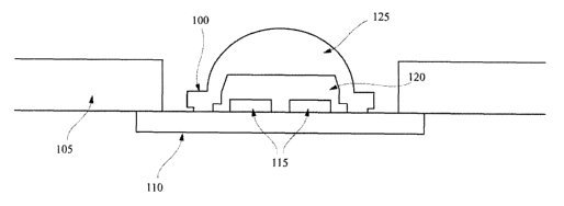
[0043] Figure 1 illustrates a lighting device package according to one
embodiment
of the present invention. The lighting device package comprises a substrate
110,
configured as a thermally conductive substrate, to which are thermally
connected light-
emitting elements 115. The lighting device package further comprises an
optical system
formed from a dome shaped lens 125 and an encapsulation material or
encapsulant 120,
wherein the optical system substantially encloses the light-emitting elements
115. In
this embodiment the space between the light-emitting elements and the dome
lens 125 is
filled with the encapsulant 120, such as an optical silicone, for example. The
encapsulant 120 can have an index of refraction as close as possible to the
light-emitting
elements to enhance light extraction.
8
CA 02613974 2007-09-21
WO 2006/099741 PCT/CA2006/000442
Substrate
[0044] The substrate provides a medium upon which one or more light-emitting
elements can be positioned. The substrate is constructed such that a thermally
conductive region is provided which may be adapted to provide intimate thermal
connection to a thermally conductive element. By positioning the one or more
light-
emitting elements proximate to the thermally conductive region of the
substrate, the heat
generated by the light-emitting elements during operation, may be transferred
away from
the lighting package though a thermally conductive element.
[0045] In one embodiment, the thermally conductive region of the substrate can
be
configured to be relatively thin, thereby reducing the thermally conductive
region's
thermal resistance to heat transfer. For example the thermally conductive
region can be
between one-half and five times the thickness of a light-emitting elements
associated
therewith. In another embodiment the thermally conductive region can be
between one
and three times the thickness of a light-emitting elements and in another
embodiment,
the thermally conductive region thickness is less than two times that of a
light-emitting
element.
[0046] The substrate can be fabricated from a number of different materials,
provided that the substrate comprises a thermally conductive region which may
provide
a means for intimate thermal connection to a thermally conductive element.
[0047] In one embodiment, the substrate can comprise two parts, namely a
carrier
portion and a thermally conductive portion. The substrate is configured for
ease of
thermal access to the thermally conductive portion. For example, the carrier
portion can
be a silicon layer upon which is formed a layer of CVD diamond or other
thermally
conductive material for example a thermally conductive ceramic selected from
A1N,
BeO, Alumina or other ceramic as would be readily understood by a worker
skilled in
the art, which forms the thermally conductive portion. In addition, alternate
thermally
conductive materials may be used for example monolithic carbonaceous
materials, metal
matrix composites (MMCs), carbon/carbon composites (CCCs), ceramic matrix
composites (CMCs), polymer matrix composites (PMCs), and advanced metallic
alloys.
The one or more layers of thermal conductive material can provide the
thermally
conductive region to which the one or more light-emitting elements can be
disposed. It
9
CA 02613974 2007-09-21
WO 2006/099741 PCT/CA2006/000442
would be readily understood that the silicon layer can be replaced by one or
more layers
of material that would be compatible with the lighting package, for example
GaAs,
GaN, AlGaS and InP.
[0048] In one embodiment of the present invention, the substrate is made
entirely of
one or more thermally conductive materials, for example, ceramic, for example
A1N,
A1203, BeO, metal core printed circuit board (MCPCB), direct bond copper
(DBC),
CVD diamond or other suitable thermally conductive material as would be known
to a
worker skilled in the art. Furthermore the substrate can be fabricated from a
metal, for
example Olin 194, Cu, CuW or any other thermally conductive alloy. The
substrate may
be coated with a dielectric for electrical isolation of one or more light-
emitting elements,
and/or electrical contacts. In one embodiment, electrical traces can be
deposited onto
dielectric coated substrate to allow electrical connectivity.
[0049] In one embodiment, the substrate can be designed with circuit traces
providing electrical connections to the one or more light-emitting elements
attached
thereto. Alternately, the electrical connections can be provided on both sides
of the
substrate. In another embodiment, the substrate can be designed to comprise
multiple
electrically conducting planes in order to reduce the required circuit traces
or other
electrical connections, for example.
[0050] The substrate can be flat, curved or configured to have any other
desired
shape.
[0051] In one embodiment of the present invention, the substrate is formed
with a
depression a central region for the positioning of the one or more light-
emitting
elements. The vertical or angled walls of the depression can be formed as a
reflective
surface thereby providing a means for further light extraction from the one or
more
light-emitting elements.
[0052] In one embodiment of the present invention, the side of the substrate
facing
the emitting surface of the lighting device package can be optically active.
For example
this surface of the substrate can be reflective in order to further enhance
light extraction
from the one or more light-emitting elements.
CA 02613974 2007-09-21
WO 2006/099741 PCT/CA2006/000442
[0053] In one embodiment of the present invention, the substrate can provide a
means for ease of thermal connection to a thermally conductive element, for
example a
heat sink, heat pipe, thermosyphon and other thermal management systems as
would be
known to a worker skilled in the art. For example, the substrate can be
configured in
order that a thermally conductive element can be provided with intimate
thermal contact
with the thermally conductive region of the substrate.
[0054] In another embodiment, the substrate can be mounted on a side of the
heat
pipe enabling thermal transmission from the light-emitting elements to either
or both
ends of the heat pipe. As would be readily understood, the substrate can
comprise one
or more thermally conductive regions and the substrate can be configured to
interconnect to one or more thermally conductive elements.
[0055] In one embodiment, the connection between the substrate and the
thermally
conductive element can be determined based on the type of thermally conductive
element being used. For example, if the thermally conductive element is a heat
pipe, the
substrate can comprise a blind bore into which the heat pipe can be inserted,
wherein the
blind bore provides a means for intimate thermal connection to the one or more
light-
emitting elements via the thermally conductive region.
[0056] In one embodiment of the present invention, intimate thermal contact
between the thermally conductive region and the thermally conductive element
can be
enhanced by the use of a thermal grease, thermal transfer film or thermally
conductive
epoxy or solder, or other thermal transfer enhancement means as would be known
to a
worker skilled in the art.
[0057] In one embodiment, as illustrated in Figure 2A, a substrate can
comprise two
components, namely a carrier portion 101 and a thermally conductive portion
109. In
one embodiment the carrier portion can be silicon upon which is formed a thin
layer
CVD diamond, wherein the CVD diamond layer can allow thermal spreading of heat
laterally and can provide a means for heat transfer to a thermally conductive
element in
intimate thermal contact thereto. As illustrated in Figures 2B and 2C, the
underside of
the silicon can be etched in order to create a circular pattern or blind bore
121 proximate
to where the light-emitting elements are positioned on the CVD diamond. This
blind
11
CA 02613974 2007-09-21
WO 2006/099741 PCT/CA2006/000442
bore can serve as a sleeve for the insertion of a heat pipe that can provide a
means for
removal of the heat generated by the light-emitting elements.
[0058] With further reference to Figures 2A and 2B, bond pads 107 and 108 can
be
positioned on the substrate and can provide positions upon which one or more
light-
emitting elements can be connected and optionally one or more sensors can be
connected. As illustrated, direct or indirect electrical connection between
the substrate
and a power supply and/or controller can be enabled by electrical contacts 141
on the
bottom of the substrate. These electrical contacts may be in the form of
solder pads, for
example. In this configuration, vias 103 and possibly electrical traces 111 on
the
substrate can be provided for enabling electrical connection of a bond pad to
the
electrical contact on the bottom of the substrate. Alternately, wrap around
connections
can be provided to electrical connection to the electrical contact on the
bottom of the
substrate.
[0059] In one embodiment of the present invention bond sites enabling
electrical
connection of the one or more light-emitting elements or one or more sensors
may be
provided on the topside of the substrate. These bond sites can provide a means
for direct
or indirect connection to a power supply and/or controller. In one embodiment,
this
configuration can provide a means for the substrate to be mounted into a
semiconductor
or integrated circuit (IC) package including quad flat pack (QFP), overmould
ball grid
array (BGA), Low profile QFP or quad flat pack no-lead (QFN), for example.
[0060] In one embodiment, a portion of the substrate can be etched to create a
micro-cooler heat exchanger that can be interfaced with a liquid cooling
system or
chiller, for example.
Light-Emitting Elements
[0061] The one or more light-emitting elements can be selected to provide a
predetermined colour of light. The number, type and colour of the light-
emitting
elements within the lighting device package may provide a means for achieving
high
luminous efficiency, a high Colour Rendering Index (CRI), and a large colour
gamut, for
example. The one or more light-emitting elements can be manufactured using
either
organic material, for example OLEDs or PLEDs or inorganic material, for
example
semiconductor LEDs. The one or more light-emitting elements can be primary
light-
12
CA 02613974 2007-09-21
WO 2006/099741 PCT/CA2006/000442
emitting elements that can emit colours including blue, green, red or any
other colour.
The one or more light-emitting elements can optionally be secondary light-
emitting
elements, which convert the emission of a primary source into one or more
monochromatic wavelengths or quasi-monochromatic wavelengths for example blue
or
UV pumped phosphor or quantum dot white LEDs or blue or UV pumped phosphor
green LEDs or other LED formats known in the art. Additionally, a combination
of
primary and/or secondary light-emitting elements can be provided within the
package,
and can be determined based on the desired light output from the lighting
device
package.
[0062] In one embodiment, a lighting device package comprises light-emitting
elements having spectral outputs corresponding to the colours red, green and
blue can be
selected, for example. Optionally, light-emitting elements of other spectral
output can
additionally be incorporated into the lighting device package, for example
light-emitting
elements radiating at the red, green, blue and amber wavelength regions or
optionally
may include one or more light-emitting elements radiating at the cyan
wavelength
region. Optionally, light-emitting elements emitting colours corresponding to
warm
white, green and blue can be selected. The selection of light-emitting
elements for the
lighting device package can be directly related to the desired colour gamut
and/or the
desired maximum luminous flux and colour rendering index (CRI) to be created
by the
lighting device package.
[0063] In another embodiment of the present invention, a plurality of light-
emitting
elements are combined in an additive manner such that any combination of
monochromatic, polychromatic and/or broadband sources is possible. Such a
combination of light-emitting elements includes a combination of red, green
and blue
(RGB), red, green, blue and amber (RGBA) and combinations of said RGB and RGBA
with white light-emitting elements. The combination of both primary and
secondary
light-emitting elements in an additive manner can be used in the lighting
device
package. Furthermore, the combination of monochromatic sources with
polychromatic
and broadband sources such as RGB and white and RGBA and white may also occur
in
the lighting device package. The number, type and colour of the light-emitting
elements
can be selected depending on the lighting application and to satisfy lighting
requirements in terms of a desired luminous efficiency and/or CRI.
13
CA 02613974 2007-09-21
WO 2006/099741 PCT/CA2006/000442
[0064] In one embodiment of the present invention the light-emitting elements
are
substantially closely packed when mounted onto the thermally conductive region
of the
substrate. This format of light-emitting element positioning can aid in the
reduction of
the amount of non-radiating surface area imaged or projected through the
optical system.
In one embodiment of the present invention, the spacing between the light-
emitting
elements can be less than about twice longest dimension of the light-emitting
element.
In another embodiment, the spacing is less than about the longest dimension,
and in a
further embodiment the spacing is less than about half the longest dimension.
In one
embodiment the spacing between the light-emitting elements is about 100 m.
[0065] In one embodiment of the present invention, the light-emitting elements
of
the lighting device package are arranged to have a relatively small
chromaticity
momentum. The chromaticity momentum can be determined as the sum of the
products
of luminous flux and distance to the optical axis for each chromaticity of the
light-
emitting elements in the lighting device package.
Optical System
[0066] The lighting device package comprises an optical system enabling light
extraction from the light-emitting elements to which it is optically coupled.
The optical
system can be formed from one or more optical elements, encapsulation
material, or
both one or more optical elements and encapsulation material. An optical
element can
be a refractive optical element, a reflective optical element, a diffractive
optical element
or other format of optical element as would be known to a worker skilled in
the art.
[0067] The optical system can be manufactured from one or more of a variety of
materials, provided that the material has desired optical and mechanical
characteristics
for the specific lighting device package. For example the optical system can
be
manufactured from one or more of polycarbonate, glass, acrylic, silicone,
metal or alloy,
reflectively coated plastic or any other material as would be readily
understood by a
worker skilled in the art.
[0068] In one embodiment, the optical system can include one or more
refractive
elements, for example, a dome lens, or a micro-lens array having one
lenticular element
per each or more light-emitting elements or a micro-lens array having more
than one
lenticular element for each light-emitting element. The refractive element can
be a solid
14
CA 02613974 2007-09-21
WO 2006/099741 PCT/CA2006/000442
glass or plastic or a fluid optical element. Furthermore the primary optical
system can
also comprise one or more diffractive or holographic elements, or one or more
diffusive
or specular reflective elements.
[00691 In one embodiment of the present invention, the optical system
comprises a
dome lens having a spherical or aspherical shape. The light emitting surfaces
of the one
or more light-emitting elements of the lighting device package are positioned
in order
that these light emitting surfaces are located at substantially the centre of
curvature of
the dome lens.
[0070] In one embodiment of the present invention, the exit aperture of the
optical
system is optimized to achieve substantially high light extraction efficiency
for a small
exit aperture size. For example, reducing the size of the exit aperture of the
optical
system can provide a means for colour mixing and beam collimation.
[0071] In one embodiment of the present invention, the optical system
comprises a
combination of one or more reflective optical elements and one or more
refractive
optical elements.
[0072] In one embodiment the optical system can be an index matching
encapsulation material. To improve light extraction, the light-emitting
elements can be
encapsulated in a transparent encapsulation material with a predetermined
optical
refractive index. For example, the encapsulation material can have a
refractive index of
about 1.4 to 2 or higher. The optical refractive index of the material can be
chosen to
substantially match the index of refraction of, for example, the light-
emitting elements.
However, commercially available encapsulation material with suitable optical
properties
typically exhibit refractive indices of about 1.4 to 1.6, which can be lower
than the
refractive indices of the materials used to manufacture light-emitting
elements, for
example semiconductor materials. Alternatively the encapsulation material can
have a
predetermined thickness and optical refractive index to increase light
extraction. The
surface of the die can be coated with a layer of encapsulation material of a
determined
thickness and optical refractive index creating an anti-reflective coating
comparable to
anti-reflective coatings used in optics manufacturing.
CA 02613974 2007-09-21
WO 2006/099741 PCT/CA2006/000442
[0073] In one embodiment of the present invention, the refractive index of the
encapsulation material is matched to the refractive index of the optical
system with
which it is in contact.
[0074] In another embodiment of the present invention, the refractive index of
the
encapsulation material is selected to be between the refractive index of the
light-emitting
elements and the optical system with which it is in contact.
[0075] In one embodiment the encapsulation material forms the optical system
and
can be patterned or textured, for example, sanded, embossed, stamped, or
otherwise
structured or micro-structured. This texturing or patterning of the
encapsulation
material can provide a means for increasing light extraction from the light-
emitting
elements, in addition to light redirection.
[0076] In one embodiment of the present invention, the encapsulant or
encapsulation
material forms the optical system and can be patterned with curved section,
pyramidal
structures, dimples or any other pattern as would be known to a worker skilled
in the art.
[0077] In one embodiment the encapsulation material may be shaped like a dome
lens or a micro-lens array by a stamping, casting or moulding process.
[0078] In one embodiment of the present invention, the lighting package
further
comprises one or more secondary optical elements that can provide a means for
further
manipulating the illumination generated by the light-emitting elements. A
secondary
optical element can provide a means for re-directing the illumination in a
desired
direction and/or can provide a means for blending the illumination generated
by the
light-emitting elements or a combination thereof.
[0079] Secondary optical elements can include one or a combination of
diffractive,
refractive, or reflective optics in order to extract the light from the one or
more light-
emitting elements, or mix the illumination to form a uniform colour, or
manipulate the
optical output of the lighting package or any combination thereof. Forms of
optical
elements can include various types of collectors, lenses, reflectors, filters,
diffusers or
other optical elements as would be readily understood by a worker skilled in
the art.
Furthermore a secondary optical element may be a liquid lens, GRIN lens and or
a
stepped compound parabolic collector, for example. A worker skilled in the art
would
16
CA 02613974 2007-09-21
WO 2006/099741 PCT/CA2006/000442
readily understand a variety of optical elements that may be used in the light
device
package and the selection thereof may be directly related to the configuration
and type of
the one or more light-emitting elements and the desired illumination to be
generated.
Sensors
[0080] In one embodiment, the lighting device package comprises one or more
sensors, wherein the one or more sensors are disposed on the substrate and
provide a
means for collecting information representative of operating conditions of the
one or
more light-emitting elements and for relaying said information to a
controller. For
example the one or more sensors can be optical sensors, thermal sensors or
pressure
sensors.
[0081] In one embodiment of the present invention, one or more optical sensors
can
provide a means for collecting information relating to the output of the one
or more
light-emitting elements, wherein this information can be quantitative
including luminous
flux and spectral information, for example wavelength. This information can
subsequently be relayed to a controller thereby providing a means for
controlling the
light-emitting elements in a desired manner thereby producing a desired level
and colour
of illumination. An optical sensor or photosensor can be selected from a
variety of
sensors including photodiodes, phototransistors, light-emitting diodes or
other optical
sensors known in the art.
[0082] In one embodiment of the present invention a single broadband optical
sensor
can be used in the lighting device package, however a multi-colour sensor may
optionally be used. Alternately, several narrow band sensors could be used to
detect the
output of the one or more light-emitting elements.
[0083] According to one embodiment of the present invention, Figure 3
illustrates
the position of an optical sensor 170 relative to a plurality of light
emitting elements
180, wherein each are mounted on a substrate.
[0084] In one embodiment, the one or more sensors can be 'intelligent' and
employ
on-board circuitry to condition their output depending on the situation. This
type, and
other types of circuitry could be incorporated with the one or more sensors to
miniaturize or adjust the output of the sensors to better suit the types of
light-emitting
17
CA 02613974 2007-09-21
WO 2006/099741 PCT/CA2006/000442
elements, the type of circuitry, or the type of controller used in the
application. For
example, photosensors can be integrated with temperature compensation,
adjustable
gain, and communication capabilities.
[0085] It would be readily understood that the collected information relating
to the
operation of the light-emitting elements can be directly related to the types
of light-
emitting elements in the lighting device package and additionally related to
the form of
optical sensor being used. For example for a lighting device package
comprising an
RGB light-emitting element configuration and a multi-colour optical sensor,
during
collection similar light-emitting elements may be pulsed in order to collect
information
relating to the optical characteristics of each colour of light emitting
element.
Alternately, if several narrow band sensors are used, optical collection
relating to the
three colours of light-emitting elements can occur simultaneously. As would be
readily
understood, filters or other optical manipulation techniques can be used to
provide a
means for collection of information relating to the operation of the various
colours of the
light-emitting elements. As would be readily understood, the size, position,
and
orientation of the one or more optical sensors could be different depending on
the
application and the information desired.
[0086] In one embodiment of the present invention, one or more thermal sensors
can
provide a means for collecting information relating to the operation of the
one or more
light-emitting elements in the lighting device package, wherein this
information can
provide a means for determining the operating temperature of the one or more
light-
emitting elements. This information can subsequently be relayed to a
controller thereby
providing a means for controlling the light-emitting elements in a desired
manner based
on the operational temperatures thereof.
[0087] In one embodiment, a thermal sensor may comprise a semiconductor diode
junction, a band gap reference circuit or any other thermal sensing element
used in the
integrated circuit art. The one or more thermal sensors can be positioned in
order to
detect the temperature of the thermally conductive region of the support
member as a
whole, or alternately a thermal sensor can be positioned proximate to a
specific light-
emitting element in order to collect thermal information of a more specific
nature.
18
CA 02613974 2007-09-21
WO 2006/099741 PCT/CA2006/000442
[0088] According to one embodiment of the present invention, Figure 4
illustrates
the position of a thermal sensor 190 and optical sensor 171 relative to a
plurality of light
emitting elements 181, wherein each are mounted on a substrate.
[0089] As would be readily understood the operating temperature of a light-
emitting
element can affect the luminous flux output in addition to the spectral output
of a light-
emitting element and therefore collecting information relating to the
operational
temperatures of a light-emitting element can enable more accurate control
thereof
thereby providing a means for creating a desired output therefrom.
[0090] In one embodiment, a thermal sensor may further be used as a safety
feature,
for example a thermal sensor can be used to protect a light-emitting element
from
overheating that can lead to premature damage of the light-emitting element.
[0091] In another embodiment, the thermal sensor is used to measure the
temperature of the light-emitting elements, and adjust the output of the light-
emitting
elements according to calibration factors, in order to maintain a certain
ratio of overall
light output, for example to maintain a particular a white point.
Electronic Components
[0092] In one embodiment of the present invention, the lighting device package
further comprises additional electronic components, for example integrated
circuits (IC),
resistors, capacitors, or other components that may provide additional
features that can
provide a means for collecting, manipulating or relaying information relating
to the
operational characteristics of the light-emitting elements to a controller.
These
additional electronic components may be mounted on, under or within the
substrate. In
one embodiment of the present invention a controller for controlling the
functionality of
one or more of the light-emitting elements can be integrated into the lighting
device
package.
[0093] In one embodiment, the substrate provides a means for connectivity to
one or
more thermally conductive elements, thereby it can additionally provide a
means for
cooling or regulating the operational temperature of these additional
electronic
components. Therefore, temperature sensitive electronic components that may
improve
the functionality of the lighting device package, for example an internal
controller, may
19
CA 02613974 2007-09-21
WO 2006/099741 PCT/CA2006/000442
be disposed on the substrate of the lighting device package of the present
invention, as
thermal management and thermal regulation can be provided.
[0094] The invention will now be described with reference to specific
examples. It
will be understood that the following examples are intended to describe
embodiments of
the invention and are not intended to limit the invention in any way.
EXAMPLES
EXAMPLE 1:
[0095] With further reference to Figure 1 which illustrates a lighting device
package
according to one embodiment of the present invention. The lighting device
package
comprises a substrate 110 configured as a thermally conductive substrate, to
which is
thermally connected light-emitting elements 115. The lighting device package
further
comprises an optical system formed from a dome shaped lens 125 and an
encapsulation
material or encapsulant 120, wherein the optical system substantially encloses
the light-
emitting elements 115. In one embodiment, the dome lens 125 can be mounted
onto the
substrate 110 using an adhesive such as silicone or a thermally or UV curable
epoxy or
other adhesive known to a worker skilled in the art. The outer dome surface of
the dome
lens can provide a means for relatively high extraction efficiency by reducing
Fresnel
reflections. Antireflection coating of the outer surface of the dome lens can
further
increase extraction efficiency provided by the optical system.
[0096] Figure 5 illustrates the substrate 110 with circuit traces 810 which
provide
electrical connection to the light-emitting elements, 820, 840 and 850
according to one
embodiment of the present invention. Each of the light-emitting elements are
mounted
on a particular first circuit trace and provided with a circuit bond 830 to a
second circuit
thereby providing independent electrical connection to each of the light-
emitting
elements. Also illustrated are fiducials 860 and pin 1 870. Pin 1 can be used
for
orientation during assembly of the lighting device package and may also be
used for test
purposes, for example. The fiducials can be provided for machine visions
systems an
can provide a means for precise orientation and position information relating
to the
package for fabrication thereof.
CA 02613974 2007-09-21
WO 2006/099741 PCT/CA2006/000442
[0097] In one embodiment of the present invention and with further reference
to
Figure 5, light-emitting elements 840 are emit green light, light-emitting
element 820
emits red light and light-emitting element 850 emits blue light. Alternate
light-emitting
element configurations, relating to the number of light-emitting elements and
colours of
light-emitting elements, would be readily understood by a worker skilled in
the art. The
alternate configurations can be dependent on the desired colour gamut of the
lighting
device package and/or the desired luminous flux output desired for the
lighting device
package, for example.
[0098] Figure 6 illustrates the substrate with circuit traces of Figure 5,
wherein light-
emitting elements 820, 840 and 850 are centred under to dome shaped lens 125.
[0099] In one embodiment, the light emitting surfaces of the light-emitting
elements
are positioned to be substantially aligned with the centre of curvature of the
dome lens.
[00100] In one embodiment, the substrate can be configured to be less than
about
twice the thickness of the light-emitting elements and the spacing between the
light-
emitting elements can be less than about half of the longest dimension
thereof. In one
embodiment the spacing between the light-emitting elements is about 100 m.
[00101] In this embodiment the space between the light-emitting elements 115
and
the dome lens 125 is filled with the encapsulant 120, such as an optical
silicone, for
example. The encapsulant 120 can have an index of refraction as close as
possible to the
light-emitting elements to enhance light extraction. Typically the refractive
index of
commercially available silicones for this type of application is in the order
of about 1.4
to 1.6. In one embodiment, the dome lens can be held in position through
adhesion with
the encapsulant 120 rather than or in addition to being adhered to the
substrate.
[00102] In one embodiment, the refractive index of the encapsulation material
can be
matched to the refractive index of the dome lens.
[00103] Electrical traces may be disposed on the thermally conductive
substrate to
provide electrical connection to the light-emitting elements. Electrical pads
on the edge
of the thermally conductive substrate can provide for the electrical and
mechanical
interfaces and can correlate to electrical pads provided on a carrier, for
example a
printed circuit board (PCB).
21
CA 02613974 2007-09-21
WO 2006/099741 PCT/CA2006/000442
[00104] The lighting device package may be coupled to a carrier 105, for
example a
PCB, wherein the coupling can be provided on the top or bottom of the carrier,
for
example. In the embodiment where the lighting device package is mounted on top
of a
carrier, electrical connection to the carrier can be provided by wrap around
connections
or vias, for example.
[00105] A secondary optic (not shown) may be mounted onto the dome lens 125 at
location 100 which may provide ease of connection therebetween.
[00106] A thermally conductive element can be positioned in intimate thermal
contact with the substrate, wherein this intimate thermal contact may be
enhanced via
thermally conductive epoxy, grease or solder, for example, thereby providing a
thermal
path to conduct heat away from the light-emitting elements in the lighting
device
package.
[00107] In one embodiment, one or more sensors or other electronic components
can
be mounted on the substrate either inside or outside the cavity provided by
the dome
lens. For example, the one or more sensors can provide information relating to
the
operating conditions of the light-emitting elements, for example, operational
temperature or luminous flux output, chromaticity of the emitted light or
other
information as would be readily understood by a worker skilled in the art.
EXAMPLE 2:
[00108] Figure 7 illustrates a lighting device package according to another
embodiment of the present invention. The lighting package comprises a
substrate 220
formed as a thermally conductive substrate, upon which is mounted light-
emitting
elements 215 and optical sensor 200. A half ball lens 210 substantially
encloses the
light-emitting elements 215 and optical sensor 200 relative to the substrate
220. The
region between the half ball lens 210 and the light-emitting elements 215 and
optical
sensor 200 can be filled with an encapsulation material or encapsulant 235.
Optionally,
a thermal sensor 236 can be positioned on the substrate 220 outside of the
region
enclosed by the half ball lens 210. Alternately a thermal sensor 237 may be
positioned
proximate to the light-emitting elements 215, and therefore may be also be
substantially
enclosed by the half ball lens 210 relative to the substrate 220.
22
CA 02613974 2007-09-21
WO 2006/099741 PCT/CA2006/000442
[00109] In one embodiment, the encapsulant can be an index matching fluid or
gel,
which can substantially match the index of refraction of the light-emitting
elements.
The encapsulant may increase the amount of light extracted from the lighting
device
package.
[00110] Figure 8 illustrates a cross section view of the lighting device
package
illustrated in Figure 7, wherein the substrate is a thermally conductive
member which is
thermally coupled to a heat pipe 230 between the two ends thereof. In this
embodiment,
the heat pipe can transmit the heat away from the light-emitting elements
towards one or
both of its ends wherein a heat sink or heat dissipation system 225 can be
connected in
order to dissipate the heat. One or more PCB boards 240 can be positioned
proximate to
the substrate thereby enabling additional electronic components to be coupled
to the
lighting device package though one or more of a variety of known electrical
coupling
mechanisms.
EXAMPLE 3:
[00111] Figure 9 illustrates another example of a lighting device package
according
to one embodiment of the present invention. The substrate 203 is formed with a
depression therein, wherein the light-emitting elements 201 can be thermally
connected
to the substrate within the depression. The side-walls 208 and the top 209 of
the
substrate can be configured to be optically active, for example reflective
which can
provide a means for additional light extraction form the light-emitting
elements and may
also provide a means for reducing re-absorption of the emitted light by the
light-emitting
elements. The side-walls 208 and the top 209 of the substrate can be specular
or diffuse
reflective or may comprise sections that are specular and diffuse reflective.
The lighting
device package further comprises an encapsulation material or encapsulant 202
comprising an embossed or pattered surface 205. This surface patterning can
provide a
means for redirecting light from the die and can also provide a means for
coupling the
light into the air outside of the lighting device package.
[00112] In one embodiment of the present invention, the optical system, namely
the
side-walls 208, the top 209 of the substrate and the encapsulant 202,
associated with this
lighting device package can be configured to redirect light away from the
light-emitting
elements, thereby reducing re-absorption of the light by the light-emitting
elements.
23
CA 02613974 2007-09-21
WO 2006/099741 PCT/CA2006/000442
EXAMPLE 4:
[00113] Figure 10 illustrates a lighting device package according to another
embodiment of the present invention, wherein the optical system is a
combination of
reflective perimeter walls 320 which are mounted around the light emitting
elements
310, and an encapsulation material or encapsulant 305 with a patterned
emitting surface
325. The sidewalls 321 of the perimeter walls 320 and the top 322 of the
substrate can
be optically active, for example to reflect the light emitted by the light-
emitting elements
310 in order to improve light extraction from the lighting device package. The
side-
walls 325 of the perimeter walls and the top 322 of the substrate can be
specular or
diffuse reflective or may comprise sections that are specular and diffuse
reflective. The
thermally conductive substrate 315 can be formed as a planar structure, for
example.
The lighting device package according to this embodiment can function similar
to that as
described for Figure 9.
[00114] Figure 11 illustrates potential interactions of light emitted by the
light-
emitting elements 401 with an optical system formed according to one
embodiment of
the present invention. Base surface 405 and side surfaces 404 can be
reflective and the
surface of the exit aperture can be patterned 403. The lighting device
packages
according to Figures 9 or 10 may produce the potential light interactions as
illustrated in
Figure 11.
EXAMPLE 5:
[00115] One embodiment of a lighting device package according to the present
invention is illustrated in Figure 12. The substrate 40 comprises two
components,
namely a carrier portion 90 and a thermally conductive portion 20. Upon the
substrate
are disposed light-emitting elements 80 in thermal contact with the thermally
conductive
portion 20 of the substrate 40. The light-emitting elements can be
electrically connected
using traces and vias 50, to bond positions 30 on the bottom of the substrate.
Furthermore the substrate is configured to enable intimate thermal contact
between a
thermally conductive element (not shown) and the thermally conductive portion
20 of
the substrate, thereby providing a thermal path for heat removal away from the
light-
emitting elements 80. In this embodiment the thermally conductive element can
be a
heat pipe and the substrate can be constructed with a blind bore 10 for
receiving the heat
24
CA 02613974 2007-09-21
WO 2006/099741 PCT/CA2006/000442
pipe therein. The blind bore however, is not specifically required, however it
can be
advantageous in that it can reduce the thermal resistance between the light-
emitting
elements and the heat pipe and may additionally provide mechanical stability.
[00116] In this embodiment, optics can be positioned over the light-emitting
elements, wherein the optics can include a moulded compound parabolic
collector
(CPC) lens 60 with an integrated holographic diffuser. In one embodiment, the
CPC
lens can be configured to surround each of the light-emitting elements
individually or
can be configured to surround all of the light-emitting elements together.
Furthermore,
the holographic diffuser and the CPC lens can be designed to reduce the
overall length
and size of the optics, while providing a desired level of light mixing of the
light emitted
by each of the light-emitting elements.
[00117] In addition an index matching substance 70, for example a fluid or
gel, can
used to encapsulate the light-emitting elements. This format of optic can
enable a high
level of light extraction from the light-emitting elements in addition to the
mixing of
different colours of light emitted by the light-emitting elements in order to
form a
desired colour of light, for example white light. The lighting device package
further
comprises one or more sensors (not shown), for example optical or thermal
sensors. An
optical sensor can be used to determine the luminous flux generated by the
light-
emitting elements and a thermal sensor can be used to evaluate the operating
temperature of the light-emitting elements.
EXAMPLE 6:
[00118] Figure 13 illustrates a lighting device package according to one
embodiment
of the present invention, wherein the lighting device package is formed as a
ball grip
array (BGA). This lighting device package comprises a BGA carrier 560, upon
which is
mounted a substrate including a silicon layer 555 and a CV diamond thermally
conductive layer 566. The light-emitting elements 540 are mounted on the CV
diamond
layer and are encapsulated by an index matching ge1545. A CPC optic 530
enables for
the manipulation of the light generated by the light-emitting elements, and
this light is
subsequently directed towards a diffuser or lens 535. This form of package can
be
encased in an epoxy resin 550, for example. The light-emitting elements can be
electrically connected to wire bends 525 which can provide a means for the
electrical
CA 02613974 2007-09-21
WO 2006/099741 PCT/CA2006/000442
connection of the light-emitting elements to solder points 527 on the
underside of the
BGA carrier though vias within the BGA carrier, for example. As is illustrated
in
Figure 13, a blind hole 565 is provided within both the BGA carrier and the
silicon layer
555 of the substrate in order to provide an insertion location for a heat
pipe. Figure 14
illustrates a modification of the embodiment illustrated in Figure 13, such
that it is
configured as a quad flat pack (QFP), wherein secondary wire bends 570 are
provided to
enable electrical connection from the QFP carrier to a proximate PCB board,
for
example.
EXAMPLE 7:
[00119] Figure 15A illustrates a lighting device package according to another
embodiment of the present invention, wherein the single configuration as
illustrated in
Figure 14, is configured as a quad flat pack (QFP) package. Furthermore,
Figure 15B
illustrates the embodiment of Figure 15A with integrated heat pipes 670, a PCB
board
640, for example a FR4 board which is positioned between the QFP package and a
support structure 650 for positioning and supporting the heat pipes. In this
embodiment
the light-emitting elements are electrically connected to the PCB board which
can have
additional electronic components mounted thereon, for example a controller. A
tertiary
optic 620 can additionally be provided and can be for example snapped onto the
package. This tertiary optic can enable further manipulation of the light
emitted from
the lighting device package, for example further light mixing.
[00120] As illustrated in the Figures, the sizes of layers or regions are
exaggerated for
illustrative purposes and, thus, are provided to illustrate the general
structures of the
present invention. Once again, as stated previously, various aspects of the
present
invention are described with reference to a layer or structure being formed on
a substrate
or other layer or structure.
[00121] It is obvious that the foregoing embodiments of the invention are
exemplary
and can be varied in many ways. Such present or future variations are not to
be regarded
as a departure from the spirit and scope of the invention, and all such
modifications as
would be obvious to one skilled in the art are intended to be included within
the scope of
the following claims.
26
CA 02613974 2007-09-21
WO 2006/099741 PCT/CA2006/000442
[00122] The disclosure of all patents, publications, including published
patent
applications, and database entries referenced in this specification are
specifically
incorporated by reference in their entirety to the same extent as if each such
individual
patent, publication, and database entry were specifically and individually
indicated to be
incorporated by reference.
27