Note: Descriptions are shown in the official language in which they were submitted.
CA 02614004 2008-01-02
~
Device and method for operating a high-pressure discharge lamp
The invention relates to a device for operating a high-pressure
discharge lamp as claimed in the preamble of patent claim 1 and
to a corresponding operating method.
I. Prior art
Such a device is described, for example, on pages 217 and 218
in the book entitled "Betriebsgerate und Schaltungen fur
elektrische Lampen" [Operating devices and circuits for
electric lamps] by C. H. Sturm and E. Klein, Siemens AG, 6th
revised edition 1992. This passage discloses the practice of
operating a high-pressure discharge lamp using a bipolar,
essentially square-wave supply current with the aid of a full-
bridge inverter, the high-pressure discharge lamp being
connected to the bridge path of said inverter.
High-pressure discharge lamps require a defined energy balance
for proper operation. If their energy balance is disrupted,
changes in the operating behavior of the high-pressure
discharge lamp result, for example a shortening of the lamp
life on account of electrode erosion or flickering caused by an
undefined discharge arc formation. When operating the high-
pressure discharge lamp using a bipolar supply current, the
zero crossing of the supply current at its polarity reversal
represents a critical operating phase of the lamp. Particularly
in the case of high-pressure discharge lamps having
comparatively thick electrodes, which have a high thermal
conductivity, for example in the case of mercury-free halogen
metal-vapor high-pressure discharge lamps, the increased
transfer of heat during the zero crossing of the supply current
gives rise to correspondingly greater cooling of the lamp
electrodes.
In this case, the power fed into the high-pressure discharge
lamp may result in insufficient heating of the lamp electrodes
prior to the polarity reversal of the supply current.
CA 02614004 2008-01-02
2
Accordingly, the lamp electrodes have a reduced emission
capability, and the voltage, which is available following the
polarity reversal, over the entire system, that is to say over
the discharge arc and the electrodes, is not sufficient to
maintain the corresponding current flow or to provide it as
quickly as possible. Flickering of the discharge arc may
therefore be observed in the high-pressure discharge lamp. This
applies, in particular, to severely aged lamps. In order to
lessen this problem, according to EP 1 176 855 A2, an
additional current or additional electrical power in the form
of a current or power pulse is injected into the high-pressure
discharge lamp close to the zero crossing of its supply current
in terms of time.
II. Summary of the invention
It is the object of the invention to provide a device of the
generic type and a corresponding method for operating a high-
pressure discharge lamp, which makes it possible to shape the
additional current or power pulse in the high-pressure
discharge lamp.
According to the invention, this object is achieved by means of
the features of patent claims 1 and 6. Particularly
advantageous embodiments of the invention are described in the
dependent patent claims.
The inventive device for operating a high-pressure discharge
lamp using a bipolar supply current and power regulation
comprises a regulator having an asymmetric regulating
characteristic curve for shaping a current or power pulse
arranged close to the zero crossing of the supply current in
terms of time. The asymmetric regulator is used to generate a
current or power pulse close to the zero crossing of the supply
current in terms of time, preferably immediately after the zero
crossing of the supply current, by the regulator immediately
counteractively controlling the reduction in the supply current
intensity or the power below a predefined desired value, which
CA 02614004 2008-01-02
3
reduction is caused by commutation, in order to increase the
supply current intensity or the power again. The regulator of
the inventive device has an asymmetric regulator characteristic
curve, with the result that it reacts to undershooting of the
desired value of the magnitude of the supply current intensity
in a more sensitive manner than to exceeding of the
abovementioned desired value. In other words, the regulator is
designed in such a manner that it reacts to undershooting of
the abovementioned desired value with comparatively faster or
greater counteractive control than in the event of this desired
value being exceeded. As a result, the regulator is used to
generate an excessive power increase in the form of a so-called
commutation pulse immediately after each zero crossing of the
bipolar supply current. The shape of this commutation pulse can
be influenced by suitable dimensions of the electronic
components of the regulator. The comparatively fast or great
counteractive control of the regulator in the event of the
abovementioned desired value being undershot gives rise to an
overshoot which determines the rise and magnitude of the
commutation pulse after the zero crossing of the supply
current. The comparatively sluggish counteractive control of
the regulator in the event of the abovementioned desired value
being exceeded prevents the occurrence of oscillations upon the
falling edge of the commutation pulse.
The asymmetric regulator is advantageously coupled to the power
regulating device which is used to regulate the power
consumption of the high-pressure discharge lamp to a constant
level. As a result, the asymmetric regulator can directly
intervene in the power regulation of the high-pressure
discharge lamp. Alternatively, the lamp current of the high-
pressure discharge lamp may also be used for regulation. The
power is preferably regulated using pulse-width modulation and
the asymmetric regulator is therefore preferably coupled to a
pulse-width modulation controller for regulating the power of
the high-pressure discharge lamp.
CA 02614004 2008-01-02
4
According to the preferred exemplary embodiment of the
invention, the device comprises a half-bridge or full-bridge
inverter, the high-pressure discharge lamp being connected to
the bridge path of said inverter in order to supply said lamp
with a low-frequency bipolar current of usually less than 1000
hertz.
The regulator is preferably in the form of either an asymmetric
proportional-integral regulator (PI regulator) or an asymmetric
integral regulator (I regulator).
III. Description of the preferred exemplary embodiments
The invention is explained in more detail below using preferred
exemplary embodiments. In the drawing:
figure 1 a) shows a schematic illustration of the temporal
profile of the supply current for the high-pressure
discharge lamp without regulation using the
asymmetric regulator,
figure 1 b) shows a schematic illustration of the temporal
profile of the power consumption of the high-pressure
discharge lamp without regulation using the
asymmetric regulator,
figure 2 shows a schematic illustration of the temporal
profile of the instantaneous power consumption of the
high-pressure discharge lamp with commutation pulses,
which are shaped by the asymmetric regulator,
immediately after each zero crossing of the supply
current,
figure 3 shows a sketched circuit of an asymmetric regulator
according to the first exemplary embodiment of the
invention,
CA 02614004 2008-01-02
figure 4 shows a schematic illustration of the temporal
profile of a regulating deviation,
figure 5 shows a schematic illustration of the response of the
regulator according to figure 3 to the regulating
deviation according to figure 4,
figure 6 shows a sketched circuit of an asymmetric regulator
according to the second exemplary embodiment of the
invention,
figure 7 shows a schematic illustration of the temporal
profile of a regulating deviation,
figure 8 shows a schematic illustration of the response of the
regulator according to figure 6 to the regulating
deviation according to figure 7,
figure 9 shows a sketched circuit of the circuit arrangement
for operating a high-pressure discharge lamp
according to the preferred exemplary embodiment of
the invention.
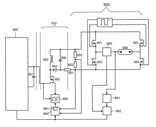
Figure 9 schematically illustrates the structure of a circuit
arrangement for operating a high-pressure discharge lamp
according to the preferred exemplary embodiments of the
inventive device. The circuit arrangement comprises a voltage
converter 900, to the DC voltage output of which a storage
capacitor 901 is connected. The storage capacitor 901 is used
as a DC voltage source for a step-down converter 910 which is
connected to it and comprises the transistor 902, the
inductance 903, the diode 904 and the pulse-width modulation
controller 905 for the transistor 902, and the capacitor 906.
The DC output voltage of the step-down converter 910 is
provided at the capacitor 906. The capacitor 906 is used as a
voltage source for the full-bridge inverter 920 which is
connected to it and is essentially formed by the transistors
921, 922, 923 and 924. The high-pressure discharge lamp 930 and
CA 02614004 2008-01-02
6
the ignition device 940 for the high-pressure discharge lamp
930 as well as the ignition monitoring circuit 941 with the
ignition timer 942 are connected to the bridge path of the
full-bridge inverter 920. The resistors 951, 952, 953 are used
to determine the instantaneous power consumption of the high-
pressure discharge lamp 930. The measurement signals from the
resistors 951, 952, 953 are supplied to the power regulating
unit 960 which generates, at its output, a control signal for
the pulse-width modulation controller 905 for the transistor
902. The power regulating unit 960 comprises a regulator 961
with an asymmetric regulating characteristic curve. Figures 3
and 6 schematically illustrate two different exemplary
embodiments of the regulator 961. However, the regulator 961
may also be implemented, in the form of software, in a program-
controlled microcontroller for regulating the power of the
high-pressure discharge lamp. The power of the high-pressure
discharge lamp 930 is regulated using the power regulating unit
960, the regulator 961 and the pulse-width modulation
controller 905 by changing the switched-on and switched-off
duration of the transistor 902 of the step-down converter 910.
The switching frequency of the transistor 902 and accordingly
also the pulse-width modulation signals generated by the pulse-
width modulation controller 905 are at a frequency above
20 kHz.
According to the preferred exemplary embodiments, the high-
pressure discharge lamp 930 is a halogen metal-vapor high-
pressure discharge lamp having a nominal power of 35 watts,
which is provided as a light source for a motor vehicle
headlamp. The circuit arrangement depicted in figure 9 is
therefore fed by the motor vehicle power supply system voltage.
The transistor pairs 921, 924 and 922, 923 of the full-bridge
inverter 920 alternately switch at a frequency of 500 hertz,
with the result that the high-pressure discharge lamp 930 is
fed with an essentially square-wave, bipolar supply current at
the same frequency. Figure la schematically illustrates the
temporal profile of an essentially square-wave, bipolar supply
CA 02614004 2008-01-02
7
current using a half-cycle. Figure lb shows the temporal
profile of the power consumption of the high-pressure discharge
lamp 930, which corresponds to the current profile illustrated
in figure la. Such a current or power profile is prior art. The
asymmetric regulator which, according to the invention, is part
of the operating device is used to generate current pulses in
the time intervals III, which current pulses are superimposed
on the essentially square-wave, bipolar supply current and
occur immediately after each zero crossing of the supply
current. These current pulses are in phase with power pulses
K1, K2 which occur in the same time intervals and correspond to
the current pulses. Therefore, figure 2 illustrates only the
temporal profile of the instantaneous electrical power
consumption of the high-pressure discharge lamp 930, which is
generated using the inventive device. The current pulses
corresponding to the power pulses K1, K2 alternately have a
negative polarity and a positive polarity and their maximum
current intensity is greater than the amplitude Imax of the
square-wave supply current. The current pulses and power pulses
(illustrated in figure 2) are also referred to as commutation
pulses Kl, K2. The regulator is in the steady state in the time
intervals I and IV before and after the zero crossings of the
supply current. The high-pressure discharge lamp 930 is
operated close to its nominal power of 35 watts during the time
intervals I and IV. The pulse power of the commutation pulses
K1, K2 and the power consumption during the phases I and IV
produce a value of 35 watts, averaged over the entire period of
the lamp current.
The commutation pulses K1, K2 during the time intervals III are
generated and shaped with the aid of the asymmetric regulator
961 which is part of the power regulating unit 960 which is
used to regulate the power consumption of the high-pressure
discharge lamp 930. The regulator 961 operates with two
different regulator characteristic curves, the first regulator
characteristic curve being effective only in the case of a
negative regulating deviation Xw, that is to say when the
desired value of the power consumption of 35 watts is
CA 02614004 2008-01-02
8
undershot, and the second regulator characteristic curve being
effective only in the case of a positive regulating deviation
Xw, that is to say when the desired value of the power
consumption of 35 watts is exceeded. The counteractive control
of the regulator 961 using the second regulator characteristic
curve is slower or more sluggish than its counteractive control
using the first regulator characteristic curve. Therefore, the
regulator 961 reacts to exceeding of the desired power value of
35 watts with weaker counteractive control than to
undershooting of the abovementioned desired power value. It is
thus asymmetric. The first regulator characteristic curve of
the regulator 961 is effective during the time intervals IIa,
IIb (figures 1 and 2) and the second regulator characteristic
curve is effective during the time intervals III.
If the supply current falls at the beginning of the time
intervals IIa when the full-bridge 920 is off, with the result
that the instantaneous power consumption of the high-pressure
discharge lamp 930 falls below the desired value of 35 watts,
the asymmetric regulator 961 is used to carry out immediate
counteractive control. The regulator 961 operates as a
proportional-integral regulator (PI regulator) or an integral
regulator (I regulator) with its first characteristic curve.
Since the clocked power supply 910, 920 of the high-pressure
discharge lamp 930 operates for a load toward zero (that is to
say its resistance value tends toward infinity) during the time
intervals IIa on account of the fact that the full-bridge 920
is off, the voltage across the capacitor 906 increases because
the energy stored in the inductance 903 discharges into the
capacitor 906 during the time intervals IIa. This excessive
voltage is available as a driving voltage during the time
intervals IIb in order to effect a steep rise in the current
intensity of the supply current at the beginning of its
negative half-cycle and to shorten the commutation time of the
supply current as well as to effect a steep rise in the power
consumption (figure 2). This results, in conjunction with the
first regulator characteristic curve of the regulator 961 which
acts during the time intervals IIb and the second regulator
CA 02614004 2008-01-02
9
characteristic curve of the regulator 961 which acts during the
time intervals III, in a severe overshoot of the power
consumption and thus in the production of the power pulses Kl,
K2 during the time intervals III. If the high-pressure
discharge lamp 930 is an old lamp which forms comparatively
long current-free phases during commutation, that is to say
during the zero crossing of the supply current, the above
effect is intensified. The regulator 961 attempts to use rapid
counteractive control in accordance with its first regulator
characteristic curve to increase the power consumption of the
lamp further. This results in a further increase in the driving
voltage across the capacitor 906 and in a more severe overshoot
and in higher commutation pulses Kl, K2.
Figure 3 schematically depicts a circuit arrangement of the
asymmetric regulator 961 according to the first exemplary
embodiment. The regulator comprises an operational amplifier
OP, two resistors Rl, R2, a diode Dl and a capacitor Cl. The
regulating variable x is supplied to the inverting input of the
operational amplifier OP via the resistor Rl. The desired value
w is supplied to the non-inverting input of the operational
amplifier OP. The output y of the operational amplifier OP is
fed back to the inverting input of the operational amplifier
via the capacitor Cl and the parallel circuit which is
connected in series with the capacitor Cl and comprises the
diode D1 and the resistor R2. This regulator is in the form of
an asymmetric proportional-integral regulator (PI regulator).
Figure 5 schematically illustrates the response of this
regulator to the regulating deviation Xw according to figure 4
which is predefined as an example. The regulating deviation Xw
is calculated as the difference between the regulating variable
x and the desired value w.
In the case of a negative regulating deviation Xw, the
regulator generates a portion P (figure 5) of the manipulated
variable y, which is proportional to the regulating deviation
Xw, and a first integral portion Ii of the manipulated variable
y. This case corresponds to the abovementioned first regulating
CA 02614004 2008-01-02
characteristic curve of the regulator 961. In the case of a
positive regulating deviation Xw, the regulator generates a
second integral portion 12 of the manipulated variable y. This
case corresponds to the abovementioned second regulating
characteristic curve of the regulator 961. Depending on the
sign of the regulating deviation Xw, the diode Dl is operated
in the forward or reverse direction and another time constant
for the RC element in the feedback path between the output y
and the inverting input of the operational amplifier OP and
thus another regulating characteristic curve as well are
correspondingly effective.
Figure 6 schematically depicts a circuit arrangement of the
asymmetric regulator 961 according to the second exemplary
embodiment. The regulator comprises an operational amplifier
OP, two resistors Rl, R2, a diode Dl and a capacitor Cl. The
regulating variable x is supplied to the inverting input of the
operational amplifier OP via the parallel circuit comprising
the resistor Rl and the series circuit of the resistor R2 and
the diode Di. The desired value w is supplied to the non-
inverting input of the operational amplifier OP. The output y
of the operational amplifier OP is fed back to the inverting
input of the operational amplifier via the capacitor Cl. This
regulator is in the form of an asymmetric integral regulator (I
regulator) . Figure 8 schematically illustrates the response of
this regulator to the regulating deviation Xw according to
figure 7 which is predefined as an example. The regulating
deviation Xw is calculated as the difference between the
regulating variable x and the desired value w.
In the case of a negative regulating deviation Xw, the
regulator generates a first integral portion Il' of the
manipulated variable y. This case corresponds to the
abovementioned first regulating characteristic curve of the
regulator 961. In the case of a positive regulating deviation
Xw, the regulator generates a second integral portion 121 of
the manipulated variable y. This case corresponds to the
abovementioned second regulating characteristic curve of the
CA 02614004 2008-01-02
11
regulator 961. Depending on the sign of the regulating
deviation Xw, the diode Dl is operated in the forward or
reverse direction and either the parallel circuit comprising
the resistors Rl, R2 or only the resistor Rl is accordingly to
be used to calculate the time constant of the RC element in the
feedback path between the output y and the inverting input of
the operational amplifier OP and two different regulating
characteristic curves, which are effective depending on the
sign of the regulating deviation Xw, thus also result for the
regulator.
The invention is not restricted to the exemplary embodiments
explained in more detail. For example, the asymmetric regulator
can also be implemented using a microcontroller or
microprocessor with implemented software, without using analog
components.