Note: Descriptions are shown in the official language in which they were submitted.
CA 02614291 2007-10-15
1
TOKEN WITH ELECTRONIC DEVICE
The present invention concerns tokens including contactless electronic
microchip identification devices, in particular gaming or casino chips.
Gaming chips are generally fabricated from rigid plastic material resistant to
scratching to obtain a robust overall structure. Gaming chips feature varied
patterns
of designs or colors to form a more or less complex decoration and to reduce
the
risks of counterfeiting and/or fraudulent reproduction. Moreover the use of
color
codes and colored patterns associated with the value of the chips, especially
on the
edge of the chips, enables croupiers or other users to identify and/or sort
chips
quickly, at a glance, even when stacked up.
To combat fraud and to facilitate counting and tracking of chips, especially
in
a gaming room or a casino, chips have been proposed incorporating inserts
including
an electronic circuit with memory in which information associated with the
chip is
stored, for example its identification number or code and/or its face value.
Communication between the electronic circuit module integrated into the chip
and its
external read/write station is usually effected without contact; a contactless
electronic
microchip identification device is then used including an electronic microchip
or circuit
associated with an antenna, generally a circular loop antenna, to enable
"contactless"
communication with the read/write station using the radio-frequency
identification
technique.
Originally the electronic microchip (or circuit) was simply connected to the
antenna by a basic electrical connection, allowing any movement of the chip in
space
relative to the antenna or vice-versa. This made the electrical connection
very fragile.
Thus attempts have been made to immobilize the microchip and the antenna in a
casing or to embed the microchip and the antenna in a mass of material to
preserve
the connection between the microchip and the antenna.
US patent 4,969,549 (Eglise) describes a payment token usable in public
telephone installations in which the electronic circuit and its antenna are
encapsulated
in a plastic material disk of small diameter, from 20 to 30 mm, the token
having a
conductive axial core passing through its center.
US patent 5,166,502 (Rendelman)describes a casino chip in which the
antenna and the electronic circuit are disposed inside a metal ballast itself
placed
between two face plates at the center of an injected plastic material ring,
the whole
being held in place by epoxy resin and by a second injection covering the ring
and the
periphery of the plates. This chip is of complex structure and costly to
manufacture,
however. Moreover, it does not offer all the necessary security in that it is
possible to
CA 02614291 2014-03-25
2
access the electronic circuit by merely cutting one face plate without
completely
destroying the structure of the chip and rendering it unusable.
The applicant has itself proposed a solution described in US patent
6,021,949, in which the casino chip includes a central disk consisting of a
rigid
plastic material shell charged with metallic particles and carrying an
electronic
identification device and an annular ring of plastic material injected around
the disk,
said plastic material possibly being charged with mineral particles. In a
first variant,
the one-piece shell is injected around a protective casing into which the
electronic
device has previously been integrated. In a second variant the shell is
obtained by
placing and fastening together the electronic identification device, a cover
and a
hollow injected plastic material disk. Although giving good results, this
technique of
manufacturing chips with electronic identification has limitations, especially
in terms
of the total thickness of a casino chip. Using this technique, it is difficult
to reduce
the thickness below 3.3 mm (for a diameter that is generally from 39 to 50 mm)
and
even virtually impossible to achieve the standard chip thickness, which is of
the
order of 3 mm.
The applicant's US patents 5,895,321 and 6,264,109 disclose chips in the
form of disks the body whereof consists of two injected plastic material half-
disks
with axial projections, defining at the center of the chip a housing for the
electronic
identifier, the two half-disks being fastened together by the edgewise
injection of a
plastic material seal.
The electronic identifier of this kind of chip is provided in particular by an
electronic circuit connected to an antenna, the circuit and the antenna being
attached to a flexible film to protect the electrical connections between the
circuit
and the antenna.
This kind of electronic identifier is still fragile, however, because of the
flexibility of the film carrying the various electronic components. Also,
these
electronic identifiers were subsequently replaced by rigid plates featuring an
CA 02614291 2014-03-25
3
electronic microchip connected to an antenna attached to the plate, preferably
by
printed circuit manufacturing methods, the plate being made from epoxy resin.
The applicant's international application WO 2007/06893 describes a chip
having this kind of rigid plate enclosed in a chip body obtained by at least
one
injection of material around said plate.
Although the chip described in the above application can be made at
relatively low cost, it is somewhat fragile, especially where the plate and
the core of
the chip are fastened together by the first injection of plastic material
around the
plate.
An object of the present invention is to propose tokens with contactless
electronic identification devices, in particular casino chips, that are
relatively
inexpensive to manufacture but are nevertheless very robust and offer improved
protection against counterfeiting.
The above object is achieved with a token including an insert comprising:
a one-piece rigid plate having a first face and a second face and forming an
electrical insulator; and
a contactless identification device attached to said first face of said one-
piece rigid plate and two protection layers obtained by injection of material,
covering at least partially said first face of said one-piece rigid plate and
said
second face of said one-piece rigid plate, characterized in that said one-
piece rigid
plate includes at least one through-hole enabling said layers to be fastened
together through said one-piece rigid plate by the formation of at least one
bridge of
material passing through said at least one through-hole and obtained by said
injection of material.
Thus the contactless identification device is trapped by the injected plastic
material. It is impossible to extract the identification device from the
insert obtained
by the first injection of plastic material without destroying the rigid plate,
and so it is
impossible to remove the identification device from inside the token without
completely destroying the token.
CA 02614291 2014-03-25
4
In a first embodiment, at least two through-holes are formed in the plate,
distributed about the center of the plate. The plate is therefore better
attached to
the two layers because a plurality of bridges pass through the plate. The
adhesion
between the two layers is strengthened by a symmetrical distribution of the
bridges.
In another embodiment, the holes have different diameters. In this way, the
diameter of the hole can vary depending on whether the hole must be made near
or
far from an electronic component. The farther the hole from a component, the
greater its diameter as the probability of damaging an electronic component
when
drilling the hole is low. It will also be noted that the larger the diameter
of the hole,
the better the layers are fastened together through the rigid plate.
The token according to the invention preferably has one or more of the
following features, separately or in combination:
- the contactless identification device includes an electronic microchip
fastened to the plate;
- said electronic microchip is covered with a protective resin, preferably a
protective varnish contributing to the temperature resistance of the
microchip;
- said contactless identification device includes an antenna produced on the
rigid plate like a printed circuit;
- the antenna is produced in the form of a winding at the periphery of the
rigid plate;
- the token includes a ballast produced by a first injection of material more
dense than that from which the remainder of the token is produced (i.e. the
portions
of the token that are neither the layers nor the insert), the dense material
being
distributed on both sides of the insert and extending in particular through
the
through-hole;
- said dense material is a plastic material charged with tungsten powder;
- said body is produced by at least one injection of plastic material around
the assembly formed by the ballast and the insert;
- said token body includes:
CA 02614291 2014-03-25
4a
- a token body core obtained by injection of plastic material and
having a central portion defining the central portion of the token body and a
peripheral portion defining at least in part the edge of said token body, and
- a covering layer obtained by a second injection of plastic material
around the peripheral portion of the core to produce with the core all or
almost all of
the edge and the peripheral portion of the token body; and
- the core defines at least in part the peripheral portion of the token body.
The invention also relates to a method of manufacturing a token including an
insert, said method comprising:
a) placing a one-piece rigid plate forming an electrical insulator and
having a
first face and a second face in a mold, said first face featuring a
contactless
identification device, said one-piece rigid plate including at least one
through-hole;
b) first injecting a material onto said first face of said one-piece rigid
plate and
onto a second face of said one-piece rigid plate to form, on each of said
faces on
both sides of said one-piece rigid plate, two layers of material, said layers
being
fastened together by at least one bridge formed by the injected material
passing
through said at least one through-hole, the resulting assembly constituting an
insert; and
c) at least one supplementary injecting of plastic material around said
insert.
Moreover, the injection of material on both sides of the rigid plate produces
a
ballast by injection of a dense material that extends on both sides of the
plate. The
token obtained in this way has the benefit of a homogeneous distribution of
its
mass relative to the median plane of its thickness.
Furthermore, it is possible to produce ballasts whose dimensions are less
than the dimensions of the rigid plate. Thus to obtain a token of
predetermined
required weight, it is possible to use different dense materials (with
different
densities) and/or to choose the dimensions of the ballast. The additional
degree of
freedom represented by the possibility of varying the dimensions of the
ballast
gives greater freedom in the manufacture of the tokens.
CA 02614291 2007-10-15
Moreover, if the ballast has dimensions less than those of the rigid plate of
the insert, then a portion of the plate projects after injection of the dense
material.
This projecting portion of the plate is advantageously used as the core of the
second
injection of plastic material so that the plastic material is attached to the
insert formed
5 by the plate and the ballast. This projecting portion of the plate also
has the
advantage of being embedded in the plastic material of the second injection so
that,
when the token is finished, extracting the identification device from the
token is
impossible without completely destroying the token.
Other advantages of the present invention will become apparent on reading
the following description, referring to two embodiments of a token according
to the
invention by way of non-limiting example, which description is given with
reference to
the appended drawings, in which:
- figure 1 represents a token according to the invention in perspective and in
section;
- figure 2 represents a rigid plate featuring a contactless identification
device
in perspective;
- figure 3 represents an. insert of a token according to the invention in
perspective;
- figure 4 represents a first embodiment of a token body molded over the
insert from figure 3 in perspective and in section;
- figure 5 represents a second embodiment of a token body molded over the
insert from figure 3 in perspective and in section.
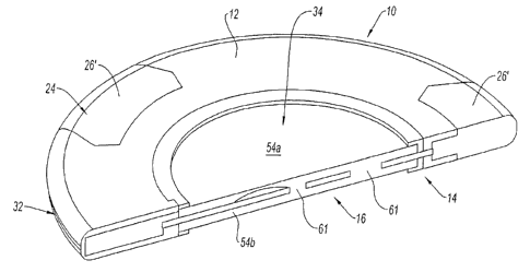
In a first embodiment of the invention, a gaming chip 10, shown in figure 1,
is
in this instance in the form of a colored plastic material disk. The chip 10
includes a
core 14 covered by a coating 12 and enclosing an insert 16.
The insert 16 is represented in figure 3 in particular, which is referred to
next.
The insert 16 includes a rigid plate 20 and two layers 54a and 54b of plastic
material that partly cover the two faces of the rigid plate 20. The two layers
54a and
54b are produced by double injection of plastic material on both sides of the
rigid
plate 20.
The rigid plate 20 is produced in the form of an epoxy resin disk and has two
faces. A contactless electronic microchip identification device 18 (figure 2)
is attached
to one of the faces.
Figure 3 shows in particular the insert 16 just after extraction from the
mold,
showing a plastic material sprue 60 attached to the layers 54a and 54b and
resulting
from the injection of plastic material via two injection points P1 and P2,
respectively,
said sprue 60 being connected to said insert 16.
CA 02614291 2007-10-15
6
Figure 2 shows only the rigid plate 20 featuring the electronic microchip
contactless identification device 18. This contactless identification device
18 includes
an electronic circuit (or electronic microchip) 40 incorporating a PROM
containing
information concerning the chip and/or the person or the object associated
with the
chip, for example a fixed numerical or alphanumerical identification code on
64 bits
(including one or more fields such as: the serial number, the identification
of a
product, a batch or a place, a numerical value associated with the chip, etc.,
and an
RF1D radio-frequency transceiver with a peripheral circular antenna 42 adapted
to be
fed by inductive coupling of modulated waves from a reading station (not
shown).
In practice, the transceiver can exchange without contact by modulated
waves data with a reading station placed at a distance (by way of non-limiting
example from 15 cm to 2 m), the operating frequency being from 10 kHz to 20
MHz.
The memory electronic device combats theft, for example and/or facilitates
the management and the inventory of a batch of objects in a defined space
(storage
areas, warehouses, stores).
Of course, without departing from the scope of the invention, the non-
reprogrammable (read-only) type memory electronic identification device can be
replaced by a reprogrammable device with code that can evolve, with the
possibility of
reading and writing in the memory.
The electronic circuit 40 is fastened to the rigid epoxy resin plate 20 and is
covered with a layer of resin or other protective varnish. This protective
varnish layer
can cover the whole of the electronic circuit 40 and can equally extend over
the whole
of the surface of the rigid plate 20 so as also to protect the antenna 42.
The antenna 42 is produced on the rigid plate 20 by standard printed circuit
fabrication methods to prevent all risk of the antenna 42 being torn off
during at least
the first molding operation carried out to obtain the insert 16.
According to the invention, the rigid plate 20 includes at least one - in this
instance four - through-holes 44. When the plastic material is injected on
both sides
of the plate, the material extends through these holes 44 to form bridges 61
fastening
the layers 54a and 54b together through the plate 20.
Because of this, the fastening of the insert 16 into the chip is more robust
than in the case of the inserts of chips of types known in the art.
Because of the presence of the bridges 61, it is impossible to extract the
plate 20 and therefore the identification device 18 without destroying the
insert 16 of
the chip.
The through-holes 44 are preferably far apart, to create connecting bridges
60 distributed over approximately all the surface of the plate.
CA 02614291 2007-10-15
7
In particular, there is provision for making holes with different diameters.
The
greater the diameter of the hole the better the layers 54 and the plate 20 are
fastened
together in the vicinity of the bridge 61 formed through the hole 44.
In the case of the embodiment shown in figure 2, the holes have different
diameters according to their location on the plate, the holes produced in the
vicinity of
an electronic component like the microchip or the antenna having a smaller
diameter
than the others, to avoid damaging the microchip or the antenna when they are
produced.
The rigidity of the plate enables the drilling of these holes. Furthermore,
because the precise position of the microchip 40 and the antenna 42 on the
plate are
known, it is possible to produce the holes accurately without damaging either
the
microchip or the antenna.
Moreover, this accuracy in the production of the plate also enables a second
antenna to be formed on the face opposite to that carrying the microchip and
the
antenna 42. The second antenna has not been shown to clarify the figures. It
is an
antenna that can take the form of a cross having the function of triggering an
alarm if
the chip is removed from a predefined geographical area, for example a room in
a
casino. Such antennas are found in particular in the "antitheft" type devices
applied to
the packaging of items in stores.
The two layers 54a and 54b preferably have a diameter less than that of the
plate 20.
As shown in figure 3, this kind of implementation produces an edge 62 of the
plate 20 projecting relative to the edge of the layers 54 between which the
plate is
sandwiched.
The projecting edge 62 has localized on its periphery a plurality of series of
four teeth 30, the series of teeth 30 being symmetrically distributed about
the axis of
the insert 16.
The teeth 30 have in particular the function of placing the rigid plate
correctly
in a mold, through the introduction of the teeth 30 into cavities formed in
the mold, or
by matching the teeth up with complementary shapes formed in the mold, for
example.
An injected plastic material peripheral ring 24 is fixed to this projecting
edge
62 and to the series of teeth 30. The insert equipped with this kind of
peripheral ring
24 constitutes a chip core. Two different embodiments of the core are shown in
figures 4 and 5.
Note in particular that the diameter of the layers produced by molding can
vary according to the shape of the ring 24 produced, fitted around the insert.
CA 02614291 2007-10-15
8
In particular, note in figure 5 that the thickness el of the projecting edge
62 is
less than that e2 of the projecting edge 62' of the chip shown in figure 4.
The peripheral ring 24 is obtained by a second radial injection of plastic
material relative to the insert 16 (radial injection is shown by the injection
point R in
figures 1, 4 and 5), which material can be a different color from the plastic
material
from which the layers 54 are made.
In this instance, the ring 24 carries at its periphery projections 26, 26'
and/or
27 extending radially and/or laterally that can be seen flush with the surface
of the
edge 32 of the chip 10 (figure 1).
In the embodiment shown in figure 5, the projections 26 are grouped in pairs
to produce a two-color pattern of colored stripes.
The embodiment shown in figure 4 provides only one projection 26' wider
than a projection 26.
It is therefore possible to produce, trapped in the mass of the body of the
chip to resist counterfeiting, colored decorations of the faces and/or edges
that can in
particular be distinguished visually, and to associate these decorations or
patterns of
colored stripes with a coding of the chips as a function of their value, for
example.
These patterns are conventionally repeated (for example 6 or 8 times) and
equi-angularly distributed, in particular on the edge 32, to enable visual or
optical
identification of the chip regardless of its orientation.
Of course, the chip according to the invention need not feature edge patterns
in the form of perpendicular stripes or patterns of stripes of color with two
projections
26. The chip according to the invention may equally feature patterns including
one to
five projections. Nor is the invention limited to two-color chips, but equally
concerns
chips with one injection, three injections or even more.
The chip may equally be decorated by fixing into a shallow central cavity 34
on each face of the chip 10 a label carrying a decoration (for example a
printed or
screenprinted decoration) and/or a mark and/or a hologram. This kind of label
has not
been shown to simplify the figures.
In the embodiment shown in figure 5, the chip need not include any central
cavity 34. In this embodiment, the ring 24 produces a shoulder 70 with the
edge of a
layer 54a of the insert, so that the layer 54a of the insert projects slightly
relative to
the surface of the ring 24 in the vicinity of the center of the chip. This
produces a
pattern different from that produced with the core represented in figure 4.
The execution of a method according to the invention is described next.
During injection of plastic material around the plate 20, the through-holes 44
formed in the rigid plate enable the insert, or at least a portion of the
insert, of the
CA 02614291 2007-10-15
=
9
chip to be produced by molding it over the identification device 18 in such a
manner
that the insert of the chip and the identification device 18 are fastened
together.
Thanks to these through-holes 44, the plastic material injected to produce
the overmolding of the identification device 18 is distributed, in the
injection mold, on
both sides of the rigid plate 20, the two layers 54 of plastic material being
fastened to
each other by bridges 61 through the through-holes 44 formed in the rigid
plate 20.
The result of this first injection is thus a unitary structure, constituting
the
insert 16, including the rigid plate 20 supporting the contactless
identification device
18 sandwiched between two layers 54a and 54b formed on respective opposite
sides
of the plate by the injected plastic material. This unitary structure makes
extraction of
the contactless identification device from the core of the chip impossible
without
destroying the insert of the chip.
The chip manufacturing process then continues with one or more injections
(overmoldings) of annular covering layers 24 around the insert of the chip to
form the
core 14 of the chip and in particular any patterns on the edge of the chip,
using
known methods.
In the context of the embodiments shown, a final injection of plastic material
is effected to produce a layer or covering 12 the surface level of which is
flush with
that of the projections 26, 26' and 27. The chip therefore has a surface and
an edge
that are totally smooth.
The chips of the invention preferably take the form of a disk with a diameter
from 39 to 50 mm and with a thickness of the order of 33 mm. The edge of the
chip
can be chamfered with rounded edges or simply with a right-angle profile,
especially if
it is wished to be able to effect optical reading from the edge of the chips.
If
necessary, the chamfered or right-angle profile is completed by trimming with
a
grinding machine or on a lathe.
The center of the central portion of the core 14 furthermore includes on each
face a central cavity 34 (figures 1 and 4). These cavities 34 correspond to
two facing
projections provided on the internal faces of the half-shells of the mold to
serve as
abutments (with a small clearance) for the electronic identifier insert 16
during
injection of the peripheral ring. These projections avoid deformation and/or
damage to
the insert 16 at the same time as preventing the risk of crushing the
electronic circuit.
The body of the chip may be made from colored plastic materials, of different
colors or not, obtained from at least one basic polymer chosen from the
following:
- polymethyl methacrylate (PMMA);
- acrylonitrile-butadiene-styrene (ABS);
- polyamides and their copolymers;
CA 02614291 2007-10-15
- polyacetal arid acetal copolymers (POM/polyoxymethylene);
- phenylene polysulfide (PPS);
- poly(alkylene terephthalate), in particular polybutylene terephthalate
(PBT);
- thermoplastic polyurethanes (PUR);
5 - vinyl polymers, polyvinyl chloride (PVC);
- polyolefins, in particular polyethylenes (PE) and polypropylenes.
In a variant of the method of manufacturing a chip according to the invention,
the material injected during the first injection, directly around the rigid
plate 20, is a
dense plastic material producing a ballast attached to the plate. This dense
plastic
10 material is a material charged with particles of tungsten, for example,
which has a
specific gravity of 4.7, 7 or 10. Thus a chip is advantageously obtained that
has the
weight required by croupiers, generally from 11 to 14 g.
Of course, the invention is not limited to the embodiments described and
numerous variants are possible without departing from the scope of the
invention.