Note: Descriptions are shown in the official language in which they were submitted.
CA 02614311 2008-01-14
WO 2007/009125 PCT/US2006/027806
MICROFLUIDIC DEVICES AND
METHODS OF PREPARING AND USING THE SAME
CROSS-REFERENCE TO RELATED APPLICATIONS
This application claims the benefit of priority from U.S. Provisional
Application Serial No. 60/699,580 filed July 14, 2005, the contents of which
are
incorporated herein by reference.
FIELD OF THE INVENTION
The field of the invention relates generally to microfluidic devices,
fabrication methods for microfluidic devices and the use of microfluidic
devices in
biological assays.
BACKGROUND OF THE INVENTION
Point of care tests, i.e., tests which are performed at the point of care
(POC),
have become common diagnostic tools used in hospitals, doctors' offices,
workplaces, and potentially hostile environments. Tasks such as workplace
testing
for drug abuse, environmental testing for pollutants, and testing for bio-
warfare
agents on the battlefield can be simply and easily performed with point of
care
tests. Since the tests are often performed by individuals having little, if
any,
clinical diagnostics training, point of care tests need to be simple, quick,
and easy
to use. Point of care tests ideally require a minimal amount of equipment.
Most current point of care tests rely on membrane-based
immunochromatography assays which take advantage of the capillary action of
microporous membranes. In immunochromatography assays, analytes in the
mobile phase specimen solutions are separated from other components by
affinity
binding to capture molecules immobilized on stationary solid phases.
Membranes,
made of nitrocellulose or nylon, provide a matrix for the solid stationary
phase of
affinity chromatography and the liquid phase of partition chromatography which
drives immunocomplex particles to be separated from other liquid solutes by
capillary action.
I
CA 02614311 2008-01-14
WO 2007/009125 PCT/US2006/027806
Microporous membranes, made of nylon or nitrocellulose, have been used
for antigen/antibody testing since about 1979 when it was first demonstrated
that
proteins could be transferred through a membrane. Nitrocellulose has been
utilized
extensively as a surface for immobilizing proteins in research techniques such
as
Western blotting and lateral-flow immunodiagnostics. Microporosity and
nitrocellulose offer many benefits for rapid immunochromatography assays
including for example, high binding capacity, non-covalent attachment of
proteins,
a stable long-term immobilization environment, and a milieu conducive to
consistent binding.
A typical prior art rapid immunoassay kit comprises a reagent pad having a
first capture antibody to which a label, such as a fluorescence label, gold
label, or
other label has been attached. A second capture antibody is attached to a
nitrocellulose or nylon membrane strip. One end of the nitrocellulose or nylon
membrane strip is placed in direct contact with the reagent pad. The second
capture antibody is often bound to the membrane to form a particular geometric
pattern, such as a line. When a sample containing analyte to be analyzed is
applied
to the reagent pad, the analyte binds to the first, labeled capture antibody
to form a
binding complex and then the solution containing the binding complex is drawn
through the membrane strip. Within the membrane strip, the complex binds to
the
second membrane-bound capture antibody. The second binding may be visualized
due to the concentration of the label along the geometric pattern comprising
the
membrane-bound capture antibody, or alternatively, the binding may be detected
through other means such as fluorescence detection, or electrochemical
detection.
Key parameters controlling signal intensity in immunochromatography
assays are capillary flow rate and protein binding capacity of the membrane.
Capillary flow rate and binding capacity are determined by the pore size,
porosity,
and thickness of the membrane. The protein binding capacity of the meinbrane
depends upon its pore size, and surface properties. Nitrocellulose membranes
are
often treated with surfactants to aid surface wetting. One concern about use
of a
surfactant is that the surfactant alters the capillary flow behavior of the
membrane
and the degree of change is difficult to predict.
2
CA 02614311 2008-01-14
WO 2007/009125 PCT/US2006/027806
The protein binding ability of the membrane and inigration speed of
particles through the inembrane depends on membrane pore size. Unfortunately,
membrane manufacturers are unable to maintain a consistent pore size and
porosity
during the production of membranes due to the complicated and delicate nature
of
the manufacturing process. High variability in pore size and porosity is
observed
between production lots, and moreover even within the same production lot. It
is
not unusual to find more than about a 20% variation in signal intensity among
different sample test kits produced under the same conditions. This
variability is a
major factor in rendering membrane-based immunoassays largely unsuitable for
quantitative testing. The high variability restricts the use of point of care
tests to
qualitative analyses. While many attempts have been made to improve the
behavior of microporous membranes, maintaining consistent quality remains a
problem.
To resolve the variability in signal intensity, many solutions have been
proposed and researched, such as improvement of the detector, alternative
labeling
of particles, and optimization of reagents formulation. Unfortunately, only a
slight
improvement in performance has resulted.
In view of the foregoing drawbacks of POC tests and their manufacture, it
would be desirable to provide more accurate POC tests and methods for
manufacturing POC tests which increase the accuracy of the tests and allow the
tests to be used for quantitative as well as qualitative analysis.
Some POC tests use microfluidic assay devices. A variety of materials
have been used to provide channels in microfluidic devices, such as silicon,
glass
and plastic. Each of those materials has shortcomings. Silicon and glass are
not
cost-effective. Silicon requires extensive chemical etching process that
inactivates
biomaterials during fabrication of micro channels and thus, is often not
compatible
with biomaterials. . Plastic is usually hydrophobic so that it requires active
transportation system to drive analytes to flow in channels, unlike porous
membrane using passive capillary action. A film type of microfluidic device
has
been designed, but it uses die cutting adhesive tape to make a fluidic channel
(see,
for example, U.S. Pat. No. 6,919,046 to O'Qoner et al., and U.S. Pat. No.
3
CA 02614311 2008-01-14
WO 2007/009125 PCT/US2006/027806
6,857,449 to Chow et al.). Alternatively, U.S. Pat. No. 6,790,599 to Madou et
al.
describes a microfluidic channel fabrication method using photolithography but
the
invention does not provide a substantially workable microfluidic device
designed
to analyze biochemical materials.
Most of immunochromatographic assays look like homogeneous assays
which are fast, one-step, separation-free, and do not require sample
pretreatment.
However, separation of the unbound ligands from those bound to the receptor is
in
the test procedure; it is named as pseudohomogeneous assay. The separation
occurs when the analyte solution passes the immobilized test line.
Electrochemical
assays are widely used for quantitative determination of small molecules such
as
glucose, lactose and inorganic materials and also applied for large molecules
because of the siinplicity and cost effectiveness of the method.
The technology has problems when applied to detect larger molecules by
one-step assay like membrane-based immunochromatography assays.
Electrochemical reactions require substrates for enzyme reactions to generate
signals. Enzymes conjugated with binding substances and substrates should be
deposited separately and supplied sequentially to avoid the self reaction
between
enzyme and substrate before binding with analyte. To perform the process, a
washing step for separation of the unbound ligands from those bound to the
receptor is required before measuring the binding level. In 1995, Ivnitski et
al
invented a one step, separation-free ampherometric inununosensor modifying a
previous enzyme-channeling immunoassay. In spite of the modification, porous
membrane-based immunochroinatographic assays do not provide a consistent flow
speed and migration time length and therefore are largely unusable for
quantitative
assays.
OBJECTS AND SUMMARY OF THE INVENTION
It is an object of the present invention to provide new and inlproved
microfluidic devices and assay kits including the saine.
It is another object of the present invention to provide new and improved
microfluidic devices that address drawbacks of current assay technology and
are
4
CA 02614311 2008-01-14
WO 2007/009125 PCT/US2006/027806
quick, inexpensive and easy-to-use, and inoreover allow for quantitative
detection.
It is yet another object of the present invention to provide new and
improved methods for fabricating or manufacturing disposable POC tests which
increase the accuracy of the tests and allow the tests to be used for
quantitative as
well as qualitative analysis.
It is another object of the present invention to provide new and improved
methods for manufacturing disposable POC tests which avoid the disadvantages
of
the prior art manufacturing techniques mentioned above.
It is another object of the present invention to provide microfluidic devices
that can provide for a consistent flow speed and migration time length.
Another object of the present invention is to provide new and improved
methods for using microfluidic devices that are designed to address the issues
associated with current assay technology and provide rapid, inexpensive, easy-
to-
use, quantitative assay systems.
Another object of the invention is to provide new and improved
electrochemical sensor devices.
In order to achieve at least one these objects and others, one embodiment of
a microfluidic device capable of conducting rapid immunoassays in accordance
with the invention is a multilayer-laminate having, for example, three layers,
namely a bottom support layer, an intermediate photoresist layer and a cover
layer.
Although any form of a support, base, substrate, layer of material or
combination
of such, may be used as the support layer, in one preferred embodiment, the
support layer comprises a polymeric film to which binding agents may be bound.
In this case, a backing substrate is attached to the support layer to provide
further
strength. The polymeric film may optionally be coated on one side, or a
portion of
one side, with a metallic film, or other coating, to which binding substances
may
be bound. The metallic film may be part of an electrode. One or more binding
substances such as biogenic or immunoreactive antibodies or antigens can be
immobilized on the polymeric film, other coating, or metallic film by direct
absorption or through binding to thin monolayers such as polypyrrole,
sulfonated
tetrafluorethylene copolymer (NAFION ), alkoxysilane or mixtures thereof. The
5
CA 02614311 2008-01-14
WO 2007/009125 PCT/US2006/027806
intermediate layer, bonded directly to the polymeric film on the same side as
the
metallic film, or other coating, comprises a photoresist film into which
inicrofluidic cliannels and chambers are etched. The photoresist film may
comprise a polyimide photoresist film such as RISTON from DuPont. Etching
may be performed by various methods well known in the art, for exainple by
photolithography. The cover layer may comprise a polymer film which may be
directly bonded to the photoresist layer to form a laminate in accordance with
the
invention.
In one embodiment, the photoresist layer includes at least three
microfluidic regions: a sample inlet chamber or region, a reagent or reaction
chamber or region, and at least one detection chamber or region. One or more
mixing regions can be provided, e.g., between the inlet chamber and the
reaction
chamber, one or more absorbent regions can be provided, e.g., downstream of
the
last detection chamber, and air vent regions can also be provided. The
chambers
and regions, when present, are connected to one another by microfluidic
channels
to form a flow path for sample fluid.
In a basic use, when a sample inlet chamber receives a liquid sample
containing an analyte to be analyzed, the liquid sample is drawn into the
sample
inlet chamber by capillary action and flows to the reaction chamber where the
sample mixes with binding reagents such as labeled antibodies. The labels may
comprise fluorescence labels, or electrochemical labels, or other labels well
known
in the art. As the sample flows out of the reagent chamber, it flows into the
detection chamber. A mixing channel may optionally be placed between the
reaction chamber and the first detection chamber. Thorough mixing of sample
and
reagents in a mixing channel insures the reaction of sample analyte and
reagents.
Typically, an iminunocomplex is formed between-an analyte and a labeled
antibody. In the detection chamber(s), an analyte-antibody complex binds to a
second antibody which is in turn directly bound to the detection chamber. The
analyte-antibody complex is thus captured and immobilized in the detection
chamber.
The amount of captured complex may be measured with a fluorescence
6
CA 02614311 2008-01-14
WO 2007/009125 PCT/US2006/027806
detector, an optical detector, or with an electrical detector. The liquid
sample may
optionally flow througli the detection chamber to the absorbent region which
can
take the form of a set of one or more absorbent channels. Liquid sample flow
continues until the absorbent region is filled with liquid. Air in the
microfluidic
system is allowed to escape through one or more air vents connected to the
detection chamber(s) or the absorbent region.
Microfluidic devices of the invention may be manufactured by in-line roll-
to-roll processes. In an exemplifying manufacturing method, the raw materials
are
three rolls, a bottom layer Polyethylene terephthalate (PET) film roll, a
middle
layer dry photoresist roll, and a top cover layer such as PET film or an
adhesive
tape roll. The rolls undergo a series of unit processes such as lamination, UV
exposure, alkaline washing, drying, adding metallic layers or other layers,
and
adding binding reagents. The three films may then be laminated together.
Finally,
the laminate may be cut to form individual laminate chips for use in rapid
immunoassays or assay kits.
Microfluidic devices in accordance with the invention have many
advantages. The materials from which the devices are fabricated are readily
available, affordable, flexible, and are as thin as the nitrocellulose
membranes
currently used in point of care iinmunoassays. The microfluidic devices of the
invention also have precisely defined flow channels insuring lot-to-lot flow
rate
consistency and allow the devices to be used for quantitative as well as
qualitative
assays.
Furthermore, microfluidic devices of the invention can easily and quickly
determine the qualitative and quantitative properties of specific analytes in
a
sample solution by analyzing the binding reaction between a pair of binding
substances, particularly biogenic or immunoreactive components and/or enzyme
reactions between a substrate and an active enzyme. These components (hapten,
specific biogenic reporters, specific biogenic ligands, antigen, antibodies,
nucleic
acids) have the ability to bind specifically to each other or react with other
molecules (enzyme, substrate, electron mediator or nucleic acids) in aqueous
test
solutions and the quantitative value of bound or reacted components can be
7
CA 02614311 2008-01-14
WO 2007/009125 PCT/US2006/027806
determined by electrochemical, fluorescent or optical detection.
An important feature of the invention is therefore the unique forination of a
series of microfluidic channels and chambers which cooperate to enable and
detennine the binding or enzymatic reaction between a pair of binding
substances
or enzyine and substrate, respectively.
In binding assay systems, the reaction chamber or region contains a dried
form of buffer reagent, biochemical reagent, antigen or antibody labeled with
gold
particles, enzymes, or a fluorescence dye. The detection chamber or region may
comprise a coating of immobilized antibody or antigen to capture the antigen-
antibody complex.
Alternatively, an electrochemical assay systein may comprise a sample
inlet chamber, a reaction chamber, at least one detection chamber, and an
absorbent region or chamber. Each detection chamber may comprise a coating of
specific enzyme or substrate which can specifically react with an analyte in
the
sample solution.
In one aspect of the invention, a liquid sample containing an analyte to be
analyzed will flow through the system until the absorbent region or chamber is
filled. The flow stops when the absorbent region or chamber is filled.
Therefore,
excess loading is not possible. This fluid flow phenomenon is typical of
capillary
flow and provides a valuable property; the precise sampling of a given test
solution.
In contrast to the unpredictable behavior of the absorbent pad of a membrane-
based assay, a microfluidic device may be used to perform a quantitative
assay.
Another advantage of the invention is that when a liquid sample comprising
an analyte to be analyzed is placed in the sample inlet chamber, liquid flows
into
the inlet chamber by capillary action, maintaining an even and constant flow
rate.
The sample reaches the reaction chamber and wets the dried reagents therein.
The
mixture flows together through the mixing chamber, undergoing a vigorous
mixing
by the engineered flow channel. The major component of the dried reagent may
comprise a labeled antigen or antibody or other analyte binding component. As
they pass through the mixing chamber, the analyte and reagent form a strong
complex.
8
CA 02614311 2008-01-14
WO 2007/009125 PCT/US2006/027806
In the detection chamber or chambers when more than.one detection
chamber is present, the liquid sample comprising the analyte complex flows
with a
lamina flow profile. In each_detection chamber resides an immobilized antibody
or
antigen or other analyte binding agent capable of binding the previously
formed
complex. Upon contact with the complex, the second binding event occurs,
resulting in the capture of the complex onto the detection chamber surface.
Unbound complexes and other free substances are washed away to the absorbent
chamber. When the absorbent region or chamber is filled, the flow stops,
enabling
the precise sampling required for quantitative assays.
Electrochemical detection of enzyme labeled antigen or antibody or other
binding complexes is well established. A silver/silver chloride reference
electrode
may be used as well as gold electrodes or carbon electrodes. Alternatively,
the
optical detection of the fluorescence from the fluorescence dye or particle
(europium or quantum particles) labeled antigen or antibody or other binding
agent
is another option.
Accordingly, microfluidic devices in accordance with the invention can
measure analytes in sample solutions, both qualitatively. and quantitatively,
through
analyzing the binding properties of the analyte and one or more binding
substances,
for example biogenic or immunoreactive substances. These binding substances
such as haptens, specific biogenic reporters, specific biogenic ligands,
antigens,
and antibodies have the ability to bind specifically to an analyte in aqueous
sample
solution. In some embodiments, the analyte comprises one or more binding
epitopes and binding at a first binding epitope does not prevent binding at a
second
binding epitope. The binding substances and analytes combine to form complexes
which may be detected by optical detection, fluorescence detection, or
electrochemical detection.
BRIEF DESCRIPTION OF THE DRAWINGS
The invention, together with further objects and advantages thereof, may
best be understood by reference to the following description taken in
conjunction
with the accompanying drawings, wherein like reference numerals identify like
9
CA 02614311 2008-01-14
WO 2007/009125 PCT/US2006/027806
elements, and wherein:
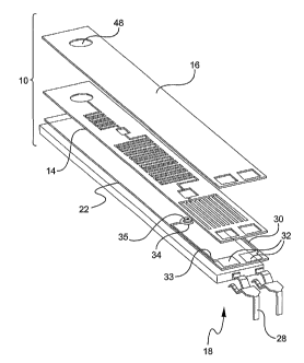
FIG. 1 is an exploded view of a first embodiment of a microfluidic device
in accordance with the invention.
FIG. 2A is a top view of the microfluidic device shown in FIG. 1 with the
cover layer removed to provide a view of the photoresist layer.
FIG. 2B is a top view of an alternative example of a microfluidic device in
accordance with the invention. 2B-1 is top view of housing encased
microfluidic
channel device.
2B-2 is fabricated micro fluidics channel device.
FIG. 2C is a top view of an alternative example of housing parts of a
microfluidic device including upper and lower housing parts in accordance with
the invention.
FIGS. 3A-3C show various alternative patterns of an absorbent region of
the photoresist layer.
FIGS. 3D-F show an alternative pattern of a reaction channel or detection
chamber of the photoresist layer.
FIG. 4 is a perspective view of the rapid assay kit including the
microfluidic device shown in FIG. 1.
FIG. 5 is a perspective view of the rapid assay kit shown in FIG. 4 with the
top housing part removed.
FIG. 6 is a cross-sectional view of the rapid assay kit shown in FIG. 4 taken
along the line 6-6 of FIG. 4.
FIG. 7 shows an example of a reading unit for use with the rapid assay kit
shown in FIG. 4.
FIG. 8 is a view of an electrochemical sensor device in accordance with the
invention.
FIG. 9 is an exploded view of the electrochemical sensor device shown in
FIG. 8.
FIGS. 10-13 show stages in the manufacture of the electrocheinical sensor
device shown in FIG. 8.
FIG. 14 is a graph showing the relationship between the rigidity of
CA 02614311 2008-01-14
WO 2007/009125 PCT/US2006/027806
photoresist film and the width of channels formed therein as a function of
exposure
time to ultraviolet radiation.
FIG. 15 shows measure points of sample fluid flow speed.
FIG. 16 is a graph showing results of sample fluid flow speed in different
microfluidic channels.
DETAILED DESCRIPTION OF THE INVENTION
Referring to the accompanying drawings wherein like reference numbers
refer to the same or similar elements, an embodiment of a microfluidic device
in
accordance with the invention is shown in FIG. 1 and designated generally as
10.
Microfluidic device 10 includes a support 22, a photoresist layer 14 arranged
above
the support 22, a cover layer 16 arranged above the photoresist layer 14 and
an
electrical interconnection unit 18 arranged in connection with the support 22.
Support 22 forms or is part of a support structure for microfluidic device 10
which can take any form which provides a preferably rigid underlying substrate
for
the photoresist layer 14. The support structure can include a base, a
substrate, and a
layer of material, either alone or various combinations thereof. In the
illustrated
embodiment, the support structure includes a rigid backing substrate 20 which
provides strength and rigidity to the microfluidic device 10 and the support
22
which is a first PET film 22 whose lower surface is directly bonded to or
otherwise
attached to the upper surface of the backing substrate 20. In one preferred
aspect
of the invention, the support 22 is a non-conductive polymeric film. A non-
limiting list of the support is selected froin the group consisting of poly-
ethylene
terephthalate (PET), polyethylene (PE) and polycarbonate. The support is
preferably PET. Backing substrate 20 maybe made of polypropylene,
polycarbonate or polystyrene plastic card. Those in the art can appreciate
other
available backing substrates to provide strength and rigidity.
Photoresist layer 14 may be made of polyimide polymer and its bottom
surface is directly bonded to or otherwise attached to the first PET film 22.
A top
surface of the photoresist layer 14 is directly bonded to or otherwise
attached to the
cover layer 16. In a preferred embodiment, the photoresist layer 14 is a dry
11
CA 02614311 2008-01-14
WO 2007/009125 PCT/US2006/027806
photoresist film, e.g., DuPont RISTON , Pyralux PC 1025, Pylalin PI2721 or SU-
8 coated film. Dry polyimide photoresist films, such as RISTON from DuPont,
are widely used for printed circuit board production in the electronics
industry.
Dry photoresist fihn is easily dissolved in weak alkaline solution. However,
upon
exposure to UV radiation, the photoresist film undergoes polymerization and
becomes resistant to dissolution in alkaline solution. In addition, once the
photoresist film has been polymerized, it is stable in aqueous solution and it
possesses good wetting properties. Such dry photoresist materials are
therefore
uniquely suited for the formation of channels, chambers, and other structures
as
discussed below.
Cover layer 16 may be a second PET film. The cover layer 16 can be a
polyineric film or adhesive film. The cover layer 16 may be transparent or
translucent. It is advantageous for the cover layer 16 to be transparent when
fluorescent or optical detection method is used. A non-limiting list of the
cover
layer 16 is selected from the group consisting of PET, polyethylene (PE),
polycarbonate, wet polyimide film or adhesive film. Cover layer 16, as well as
the
other cover layers in microfluidic devices disclosed herein, is also referred
to
herein simply as a cover.
In some preferred aspects of the invention, electrical interconnection unit
18 is designed to electrically connect a region of the photoresist layer 14
(the
specific region is discussed below) to a reading unit 24 which engages with a
housing 50 in which the microfluidic device 10 is enclosed (see FIG. 7).
Electrical
interconnection unit 18 includes electrodes 30 and 33. Electrical
interconnection
unit 18 further coinprises a pair of, for example, substantially L-shaped
connector
pins 28 made of an electrically conductive material. Electrodes 30 and 33 are
formed on or in connection with the first PET film 22 by a known manufacturing
process, such as photolithography, screen printing or sputtering method. For
example, part of the electrodes 30 and 33 coinprise the form of a metallic
film
which is photolithographically patterned around a designated part of the
photoresist layer 14 and leads extending from this metallic film to the pins
28.
Preferably, the electrodes 30 and 33 are directly bonded to the upper surface
of the
12
CA 02614311 2008-01-14
WO 2007/009125 PCT/US2006/027806
first PET film 22.
The conductive or metallic materials used in the electrical interconnection
unit 18 may be gold, indium tin oxide (ITO), silver, platinum, palladium
either
individually or mixtures thereof. When microfluidic device 10 is used for
fluorescent or optical detection, electrical interconnection unit 18 is
unnecessary.
In one exemplifying construction of the invention, electrodes 30 and 33 are
substantially U-shaped and have an electrode pad 32 at one end which is in
direct
contact with a respective connector pin 28. At an area opposite the pads 32,
working portions 34 and 35 of the electrodes 30 and 33 are below a designated
part
of the photoresist layer 14. It should be understood that the shapes of the
pads 32
and working portions 34 and 35 are one example and are not limited to that
particular shapes in FIG. 2A. Cover layer 16 has apertures aligning with the
pads
32. The apertures in photoresist layer 14 and cover layer 16 preferably allow
a
portion of the electrodes 30, 33 to be exposed to allow for contact with the
connector pins 28 as shown in FIG. 2A. One of the electrodes 30, 33 is to
perform
as a working electrode and the other as a reference electrode, the use of
which is
well appreciated by those skilled in the art.
Electrodes may be made of any electrically conductive material, including
but not limited to, gold, indium tin oxide, silver, platinum, palladium and
combinations of these materials.
In one example of connector pins 28, connector pins 28 have separated
flanges which engage with opposite sides of the support PET film 22 and the
backing substrate 20 to press the pads 32 against the backing substrate 20 and
thereby provide for a secure electrical connection between the connector pins
28
and the pads 32. Alternative electrical engagement mechanisms which create an
electrical path from the pads 32 to pins can be used in the invention without
deviating from the scope and spirit thereof.
In an exemplifying construction of microfluidic device 10, the thickness of
the cover and support PET films 16 and 22 is approximately 100 m thick. The
thickness of the photoresist layer 14 is from about 25 to about 100 m, and is
preferably, approximately 50 m thick. As such, one preferred microfluidic
device
13
CA 02614311 2008-01-14
WO 2007/009125 PCT/US2006/027806
has a thickness of about 250 m above the backing substrate 20. The thickness
of the electrodes 30, 33 is preferably less than 50 m and should be less than
that
of the photoresist layer 14 in microfluidic device 10. The thickness of the
electrodes 30, 33 can be more preferably from about 2 to 20 m. When the
5 electrode material is ITO, the electrode can be as thin as 2 m.
FIGS. 2B and 2C illustrate alternative construction of microfluidic devices.
Referring to FIG. 2B, microfluidic device 210 includes a support 222, a
photoresist layer 214 arranged above the support 222, a cover layer 216
arranged
above the photoresist layer 214 and an electrical interconnection unit 218
arranged
10 in connection with the support 222.
Alternatively, the cover 216 consists of two sheets having a junction gap
201 between the two sheets. The junction gap 201 is similar to the delay
channel
38 in FIG. 2A serving to incorporate a delay or time-lag into the analyte
testing,
and is useful for flow stabilization. The junction gap is, however, not too
wide to
cause leakage of sample fluid. Reaction region 240 is placed within a channel
connecting a sample inlet 236 and a mixing region 242.
Electrical interconnection unit 218 includes electrodes 230 and 233. At one
end of each of the electrodes 230 and 233, working portions 234 and 235 of the
electrodes are below a designated part of the photoresist layer 214 which
defines
the detection chamber 244.
The length of cover layer 216 is less than of the photoresist layer 214 and
thus, a portion of the electrodes is exposed to allow for contact with the
connector
pins (not shown in this embodiment but which may be the same as described
above). Open ends of a set of an absorbent channel form air vents. The length
of
the cover layer 216 at the electrode pads is preferably, slightly less than
the
photoresist layer 214 and favorably allows air vents.
Referring to FIG. 2C, microfluidic device 310 includes a support 322, a
photoresist layer 314 arranged above the support 322 and a cover layer 316
arranged above the photoresist layer 314. Microfluidic device 310 includes a
junction gap 301 between the two sheets of the cover layer 316. In some
preferred
aspects of the invention, a microfluidic device allows multiple analytes to be
tested
14
CA 02614311 2008-01-14
WO 2007/009125 PCT/US2006/027806
simultaneously. Such a inicrofluidic device may include two or more detection
chambers or regions. In one preferred exemplifying construction, microfluidic
device 310 contains three detection chambers or regions 344 (see FIG. 2C). One
of the three detection chambers may be for a reference and the others for
analytes
to be analyzed. Each detection chamber 344 can include a different substance
bonded to the metallic film or polymeric film. Hydrophobic and electrostatic
interactions between the substance and the metallic film or polymeric film are
enough to prevent the substance from being washed and flowing to absorbent
channels. Alternatively, the substance can be bonded to the metallic film or
polymeric film coated with self-assembled inonolayer such as polypyrrole,
sulfonated tetrafluorethylene copolymer (NAFION ), alkoxysilane or mixtures
thereof. These self-assembled monolayers (SAM) enhance the binding efficiency
and strength. The substance is preferably bonded to the self-assembled
monolayer
coating the metallic electrode, ITO or polymeric film. To immobilize
antibodies or
capture molecules on the metallic electrode or polymeric film in the detection
chamber, the surface of the metallic electrode or polymeric film may be
modified
with self-assembled monolayers (SAM) or by hydrophobic polymer printing. The
SAM is a unidirectional layer formed on the surface caused by spontaneous
aggregation of SAM-forming molecules.
Thiol-containing SAM-forming molecules are one of the well-established
binding molecules to gold. Carboxyalkanethiol compounds and succinimidyl
alkanedisulfide compounds (succinimidyl ester-terminated
alkyldisulfides) are widely utilized for forming SAM on the gold surface to
introduce carboxylic groups or amine reactive sites. Succinimidyl ester-
terminated
alkyldisulfides are amine-reactive analogs of carboxyalkyldisulfide. The
carboxyl
groups of carboxyalkanethiols are converted to activated N-hydroxysuccinimide
ester to bind to ainines of antibodies or capture molecules. The surface
coated with
SAM does not require any other coupling agents to immobilize antibodies or
capture molecules. The SAM-forming molecules are applied on the surface of the
gold electrode or polymeric film by spotting and drying process.
The cover layers 216, 316 in the einbodiments shown in FIGS. 2B and 2C
CA 02614311 2008-01-14
WO 2007/009125 PCT/US2006/027806
form junction gaps 201,301 which provide for flow time delays between the
reaction chamber 240, 340 and mixing channel 242, 342, respectively.
Referring now to FIG. 2A, the photoresist layer 14 has a unique structure
which provides for a simple and efficient analyte testing. Specifically, when
formed in a manner described below, the photoresist layer 14 is provided with
a
distinctive pattern of chambers and channels which cooperate to allow for an
expeditious analyte testing. FIG. 2A shows an exemplifying pattern wherein the
photoresist layer 14 includes an inlet chamber 36 at one end, a delay channel
38
connected to the inlet chamber 36, a reaction chamber 40 connected to the
delay
channel 38 and which contains a reagent mixture including a first analyte
binding
substance, a mixing channel 42 connected to the reaction chamber 40 which also
preferably contains the first analyte binding substance, a detection chamber
44
connected to the mixing channel 42 and a set of absorbent channels 46
connected
to the detection chamber 44. Although shown in a linear fashion, the various
chambers and channel can be positioned in other arrangements, including in a
non-
linear arrangement. The set of absorbent channels 46 may contain only a single
channel or a plurality of channels, examples of which are discussed below and
also
shown in FIGS. 2B and 2C.
Inlet chamber 36 is that part of the photoresist layer 14 into which a fluid
to
be tested is placed. Cover layer 16 is provided with an aperture 48 aligning
with
the inlet chamber 36 in order to avoid inhibiting the flow of fluid into the
fluid
chamber (see FIG. 1).
Delay channel 38 serves to incorporate a delay or time-lag into the analyte
testing, and is also useful for flow stabilization, i.e., stabilizing the flow
of the
sample fluid. Delay channel 38 is formed from a series of transverse sections
and
longitudinal sections connecting adjacent transverse sections to thereby form
a
meandering path.
Mixing channe142 is formed from a series of transverse sections extending
across a substantial portion of the width of the photoresist layer 14 and
longitudinal
sections connecting adjacent transverse sections to thereby form a meandering
path.
The working portions of the electrodes 34 and 35 are arranged in or form at
16
CA 02614311 2008-01-14
WO 2007/009125 PCT/US2006/027806
least a part of the detection chamber 44. Thus, the part of the photoresist
layer 14
aligning with the working portions 34 and 35 is the detection chamber 44.
The set of absorbent channels 46 includes elongate longitudinal sections
and a transverse distribution section extending across the upper ends of the
longitudinal sections. An inflow section from the detection chamber 44 leads
to an
intermediate location on the transverse distribution channel.
Variations in the set of absorbent channels 46 are shown in FIGS. 3A, 3B,
3C. Depending upon, for example, the particular test being performed, the
width
and length of the channels and the volumes of chambers may be varied. In a
test
that requires washing process, the absorbent channel volume should preferably
be
larger than the total volume of other part of channel and chamber, preferably
about
three times larger than the volume of the other part of the channel.
The width of microfluidic channels 38, 42 and 46 may vary from about 50
microns to about 1000 microns and is preferably from about 50 microns to 500
microns, and more preferably about 300 microns. The height of the channel may
vary from about 25 microns to about 300 microns and is preferably about 50
microns
The channels 38, 42, 46, as well as the chambers 36, 40 and 44, are defined
by parts of the support 22 (the bottom of the channels and chambers), parts of
the
photoresist layer 14 (the walls of the channels and chambers) and parts of the
cover
layer 16 (the top of the channels and chambers). Laminating the support 22,
the
photoresist layer 14 and the cover layer 16, e.g., in the manner described
below,
provides for a well-defined flow path through the microfluidic device 10.
The intermediate layer 14 is a dry photoresist film that provides the
precisely defined micro fluidic channel structure. The intermediate film
comprises
a negative photoresist material with a typical thickness of 50 micron. The
film
uncovered with a mask is polyinerized under a strong UV light resulting in an
insoluble polymer film. Masked areas of the film are easily etched away by a
spray of an alkaline solution. The surface of the polymerized, hardened film
is
hydrophilic, a benefit of this device.
In FIGS. 3A, 3B and 3C, the set of absorbent channels 46, 246 and 346
17
CA 02614311 2008-01-14
WO 2007/009125 PCT/US2006/027806
includes elongate longitudinal sections and a transverse distribution section
which
extends across the upper ends of the longitudinal sections. The inflow section
leads from detection chamber 44 to the transverse distribution channel.
In FIGS. 3D and E, the set of reaction channels includes a single channel
having a series of elongate longitudinal sections and short connecting
transverse
sections to thereby form a meandering path.
In FIG. 3G, the set of channels includes a series of oval sections to adjust
flow speed of sample solution.
In FIG. 3F, the set of channels having a series of longitudinal sections and
connecting transverse sections to thereby form a meandering path, with an
enlarged chamber being formed in the middle of the channel.
As shown in FIG. 2A, the reaction chamber 40 and detection chamber 44
have substantially rectangular configurations. Alternatively, these chambers
can be
formed as shown in FIG. 3G as a progression of increasing diameter circular
regions. Air is released from the chambers and channels in the photoresist
layer 14
through air vent areas connected to the detection chamber 44 and/or the set of
absorbent channels 46. Open ends of one or more of the absorbent channels 46
may form or include air vent areas.
Microfluidic device 10 would typically be installed into a housing, for
example, made of plastic, to thereby form a complete robust rapid assay kit.
At a
minimum, the housing inust allow for insertion of a fluid to be tested into
the inlet
chamber 36 and preferably visualization of the detection chamber 44 (to ensure
that at least a portion of the fluid being tested has reached the detection
chamber
44). Such housing can take multiple forms.
One such housing is shown in FIGS. 4-6, wherein the microfluidic device
10 is placed into housing 50 which has an upper housing part 52 and a lower
housing part 54. Lower housing part 54 includes a planar base 56, a peripheral
wall 58 extending upward from the base 56 and defining a recessed area 60, and
positioning ridges 62 formed an on inner surface of the base 56 and spaced
apart
froin one another to accommodate the backing substrate 20 therebetween. Lower
housing part 54 also includes a mating structure 64 to enable it to engage
with a
18
CA 02614311 2008-01-14
WO 2007/009125 PCT/US2006/027806
complementary mating structure on the upper housing part 52, e.g., apertures
in the
upper housing part 52.
Lower housing part 54 is also formed with a pair of apertures (not shown)
in the base 56 through which the connector pins 28 extend to the exterior of
the
housing 50 in order to enable electrical interconnection to electrical
contacts on the
reading unit 24 (shown FIG. 7). Instead of L-shaped pins 28, pins 28 can be
constructed without a perpendicular bend and thus would extend directly away
from the microfluidic device 10 in which case, apertures for passage of these
pins
to the exterior of the housing 50 would be provided in one or both of the
lower
and/or upper housing parts 52, 54. In the kit 24, those skilled in the art
will
appreciate that alternative electrical contacts on the reading unit 24 can be
used in
the invention without deviating from the scope and spirit thereof.
Prior to engagement of the upper and lower housing parts 52, 54 together to
housing 50, a filter 66 is placed over the inlet chamber 36 to filter the
fluid being
tested (see FIG. 5). Filter 66 (and filters 266, 366) is constructed to remove
any
particles that may cause interference of binding signal generation or blockage
of
the microfluidic channels in the photoresist layer 14.
Upper housing part 52 includes a substantially planar base 68 having a
sample well 70 aligning with the aperture 48 in the cover layer 16 and thus
the
inlet chamber 36. Base 68 may include a detection chamber window 74 which is
positioned to align with the detection chamber 44. Base 68 can further include
a
reaction chamber window 72 which is positioned to align with the reaction
chamber 40. To enable the reaction chamber 40 and detection chamber 44 to be
viewed through windows 72, 74, the cover layer 16 could be made of a
transparent
material. In some preferred aspects of the invention, the transparent cover 16
and
detection chamber windows 74 are advantageous when a fluorescent or optical
detection method is used. The wetting of the dried reagent may be monitored at
the reaction chamber window 72 and a visual inspection of the detection
chamber
44 may be made through the detection chamber window 74.
In the embodiments where more than one detection chamber is presented,
e.g., FIG. 2C wherein three detection chambers 344 are provided, the base 68
19
CA 02614311 2008-01-14
WO 2007/009125 PCT/US2006/027806
preferably includes a detection chamber window for each detection chamber 344
as
shown in FIG. 2C.
Use of the kit 26 as a test for an analyte having one or more epitopes to
which binding substances may bind where substance binding to the first epitope
does not prevent substance binding to the second epitope will now be
described. A
sainple of a liquid to be tested is obtained and placed into the sample well
70, onto
the filter 66, so that it flows through the filter 66 into the inlet chamber
36. The
liquid sample is drawn from inlet chamber 36 through the delay channe138 to
the
reaction chamber 40 and interacts with the first analyte binding substance in
the
reaction chamber 40. The first binding substance is placed in or on the
reaction
chamber 40. As the liquid sample wets the reagent mixture in the reaction
chamber 40, analyte reacts with the first analyte binding substance forming a
first
analyte-binding substance complex, the first analyte binding substance binding
to a
first epitope of the analyte. From the reaction chamber 40, the liquid sample
then
flows into the mixing channel 42 in which any unreacted analyte is contacted
with
a first analyte binding substance. Upon exiting the mixing channe142, the
liquid
sample enters the detection chamber 44. The second analyte binding substance
on
the working portion of the working electrode in the detection chamber 44,
binds a
second epitope of analyte, thereby capturing the complex of first analyte
binding
substance and analyte.
As liquid sample continues to flow, it exits from the detection chamber 44
and enters into the set of absorbent channels 46. Unbound protein, complexes,
reagents and other components of the liquid sample flow through the detection
chamber 44 into the set of absorbent channels 46. Once the set of absorbent
channels 46 is filled, the flow of liquid sample ceases.
Binding of the first analyte binding substance-analyte complex to the
second analyte binding substance captures the complex. Binding of the complex
to
the second analyte binding substance changes the capacitance, impedance,
resistance or current of the electrode 30 and (electrical status change). The
inagnitude of the electrical status change on electrode is related to the
degree of
binding and therefore related to the amount of analyte present in the liquid
sample.
CA 02614311 2008-01-14
WO 2007/009125 PCT/US2006/027806
Since electrodes 30 and 33 are in electrical contact with the pads 32, which
in turn
are in electrical contact with the connector pins 28, the difference in the
magnitude
of the electrical status change between the working electrode and the
reference
electrode is measurable by connecting a capacitance, impedance or ainperometer
to
the connector pins 28. Such an electrical detection reader is present in the
reading
unit 24 which includes a pair of electrical contacts for electrically
connecting to the
connector pins 28 and electrical interconnection structure for connecting
these
contacts to the detection reader. Those skilled in the art will appreciate
that the kit
26 may include a calibration electrode.
A more specific use of the kit 26 would be as a proposed
immunoelectrocheinical assay device to show the performance mechanism of a
one-step immunoassay device for Acute Myocardial Infarction test.
Chest pain may arise from a variety of causes, for example a heart muscle
problem. When a small blood clot forms in a heart blood vessel, chest pain may
occur. If the clot is dissolved, the pain disappears. If the clot persists,
the blood
vessel may become blocked and a portion of the heart muscle may be denied
oxygen and nutrients. Dying heart muscle cells release Troponin I, therefore
elevated levels of Troponin I often indicate a heart muscle problem. Checking
the
Troponin I level of a patient complaining of chest pain can therefore aid in
the
diagnosis of the problem. A microfluidic device of the invention can be used
to
construct a Troponin I test kit.
For such a test kit in which Troponin I is selected as the analyte, in the
reaction chamber 40, dried anti-Troponin I antibody labeled with indicating
molecules, mixed with detergents 0.01 % of tween 20, buffer reagent 10mM of
sodium phosphate pH 7.2 and a stabilizer 0.5% trehalose, 0.5% BSA and 0.5%
PEG is deposited. In the detection chamber 44, the second anti-Troponin I
antibody is immobilized on the surface of electrode by covalent or noncovalent
bonding and will bind with a different epitope of the Troponin I. A second
anti-
Troponin I antibody is diluted to a concentration of 30 g/ml - 3mg/ml in 10
mM
phosphate buffer containing 0.5% BSA. The second anti-Troponin I antibody
solution is spotted on the surface of the electrode in the amount of 50 1-100
l per
21
CA 02614311 2008-01-14
WO 2007/009125 PCT/US2006/027806
cm2 and is dried at 25 C and 40% humidity for 1 hour.
During use, when approximately 5-10 microliters of whole blood sample
fluids containing Troponin I is placed in the sample well 70, the plasma
sample
fluids pass through blood separation filter 66 into inlet chamber 36 and flow
through delay channel 38 to the reaction chamber 40. As the plasma wets the
dried
reagents in the reaction chamber 40, the Troponin I antibody and the Troponin
I
forms an antigen-antibody complex and flows into the mixing channe142. Any
unbound antibody is bound to Troponin I molecules with the aid of the mixing
effect in the mixing channel 42. In the detection chamber 44, a second
Troponin I
antibody is immobilized on the surface of the electrode and will bind with a
different epitope of the Troponin I. When the fluid passes into the detection
chamber 44, the antigen-antibody complexes bind to the second antibody
therein.
The unbound complexes and other substances are washed away with the
continuous stream of the sample fluid. The sample fluid enters the set of
absorbent
chamlels 46 until the set of absorbent channels 46 is filled with plasma.
Then, the
sample fluid flow stops and the immunochemical reaction stabilizes in the
detection chamber 44.
The ainount of the captured antigen-antibody complex on the electrode
surface is related to the capacitance or voltage change of the working
electrode 30.
When the antigen-antibody complex is captured, it causes a slight change of
the
capacitance of the electrode 30. The capacitance change may be measured with a
capacitance meter when the rapid assay kit 26 is inserted into a reading unit
24.
Reading unit 24 is designed to covert the electrical status change into a
reading
indicative of the presence of amount of Troponin I antigens.
The foregoing is only a single example of a use of the kit 26 including
microfluidic device 10 in accordance with the invention. Other detection
methods
which can be implemented using kit 26 with microfluidic device 10 include
fluorescence, optical coloring, amperometric, ampedance/potentiometer and
particle assay.
For fluorescence detection, the deposited reagents in the reaction chamber
are binding substances, i.e., antibodies or antigens coupled with fluorescence
22
CA 02614311 2008-01-14
WO 2007/009125 PCT/US2006/027806
dye or particles such as quantum or europium. The binding substances
immobilized in the detection chamber 44 are capture antibodies or antigens.
For
optical coloring, the deposited reagents in the reaction chamber 40 are
antibodies
or antigens coupled with oxidation or reduction enzyme. For amperometric
detection, the deposited reagents in the reaction chamber 40 are antibodies or
antigens coupled with horseradish peroxidase (HRP) enzyme and glucose as a
substrate. The materials immobilized in the detection chamber 44 are capture
antibodies or antigens, and glucose oxidase on the electrode 30. Antibodies or
antigens coupled with alkaline phosphatase (APase) enzyme can be deposited in
the reaction chamber 40. Other variations of the above are contemplated and
well
understood by those skilled in the art.
For impedance/potentiometer uses, there are no deposited reagents in the
reaction chamber 40. The binding materials immobilized on the electrode 30 are
capture antibodies or antigens. In this case, the delay channe138 and reaction
chamber 40 can be eliminated. Those skilled in the art will appreciate that
binding
substances in the reaction chamber 40 and detection chamber 44 can be one or
more biogenic or immunoreactive substances capable of forming a complex, such
as antibody/antigen, antibody/hapten, enzyme/substrate, reporter/hormone,
nucleotide/nucleotide.
When microfluidic devices 10 in accordance with the invention are used for
optical coloring or amperometric detection methods, the active substrate
hydrogen
peroxide for HRP enzyme is generated by coimmobilized glucose oxidase on the
conductive surface of the electrode 30 with capture antibody. The glucose and
HRP-conjugated antibody is placed in dry form in a location at the front of
the
reaction chamber 40 where the binding reaction occurs. Sample solutions will
solublize the dried reagents and move them to the reaction chainber 40., To
increase the binding sensitivity, streptavidine or avidine might be
immobilized on
the electrode instead of a capture antibody. In this case the HRP-conjugated
antibody and second capture antibody coupled with biotin is placed at the
reaction
chamber 40.
The detection methods discussed above are merely exemplifying detection
23
CA 02614311 2008-01-14
WO 2007/009125 PCT/US2006/027806
methods and their mention does not liunit the scope of invention but simply
provide
examples of currently preferred embodiments of the invention.
As shown in FIG. 7, reading unit 24 is designed to read an electric signal
when the assay kit 26 is inserted into a slot therein. Reading unit 24
includes a
housing 76 defining the slot, a display 78, a button 80 and a processor or
inicrocontroller arranged in the housing 76. Reading unit 24 also includes
electrical contacts designed to engage with the pins 28 and connect to the
microcontroller to enable the formation of a circuit including the electrodes
30 and
33. Upon insertion of the assay kit 26 into the slot defined by housing 76,
the
button 80 is pressed to direct the microcontroller to fonn the circuit
including
electrodes 30 and 33 and detect the electrical status change. The electrical
status
change is correlated with the assay result which is displayed on display 78.
More
specifically, the microcontroller in the reading unit 24 produces a digital
signal
when the kit 26 is placed in contact with the contacts of the reading unit 24
and the
button 80 is pushed by the user.. The reading unit 24 may be calibrated to
produce
displayed results meaningful to users of the system.
Depending on the substances, if any, arranged in the reaction chamber 40,
if present, and the detection chainber 44, and the construction of the reading
unit
24, the microfluidic devices 10 in kits 26 in accordance with the invention
may be
used in the following types of assays:
1. Drug Abuse assays for analytes such as heroin, morphine, cocaine,
LSD, amphetamines, PCP, THC, barbiturates, and other sedatives, narcotics, and
hallucinogens.
2. Infectious disease assays, such as Streptococcus A, HIV, Hepatitis
A, B and C virus, H. pylori, Mononeuclosis, Chlamydia, Gonorrhea and other
STDs.
3. Therapeutic Drug Monitoring
4. Reproduction related testing including hCG, FSH, and LH
5. Diabetes testing, such as monitoring glucose, HblAc levels in blood
6. Cardiac markers, such as CK MB, Troponin, Myoglobin, BNP, pro
BNP, hCRP, D-dimer, homocystein
24
CA 02614311 2008-01-14
WO 2007/009125 PCT/US2006/027806
7. Cholesterol monitoring, such as HDL, LDL, and ApoLP
8. Blood Coagulation Testing
9. Cancer Markers, such as CEA, AFP, PSA, BladderCa (BTag)
10. Osteoporosis monitoring such as bone resorption testing
11. Mental Disorders, such as Alzheimers disease test detecting
isoprostane, and neural thread protein
12. DNA diagnostics for genetic testing using micro array and PCR
devices
13. Allergy testing
14. Urine analysis
15. Blood Gas/ Electrolyte
16. Animal health testing
Microfluidic device 10 can be manufactured in a variety of ways. One non-
limiting manufacturing method is to first select a support 22, such as a PET
film,
then print electrodes 30, 33 on the PET film, cover the electrodes 30, 33
printed
PET film with a polyimide photoresist film, such as DuPont RISTONO to be used
to form photoresist layer 14, then cover the photoresist film with a
protective
covering with a photomask which has an outline of a pattern of channels and
chambers, polymerize the photoresist material through exposure to UV light,
remove the protective covering, wash away the unexposed, masked photoresist
film with alkali solution, apply any necessary reagents, and cover the
photoresist
layer 14 with a cover layer 16. The cover 16 is a nonconductive polymeric
fihn.
An adhesive film can be used as the cover layer 16 securing the photoresist
layer
14.
The cover layer 16 may be a second photoresist film having its protective
cover removed, and which is placed in direct contact with the first
photoresist layer.
The second photoresist layer is bonded to the first photoresist layer, for
example,
upon application of heat. During the laminating process, temperatures within a
range of about 45 C to about 110 C may be used, preferably about 90 C. Heat
exposure times may vary depending on sizes of heat pressure rollers within a
range
of from about 5 seconds to about 500 seconds, preferably less than about 30
CA 02614311 2008-01-14
WO 2007/009125 PCT/US2006/027806
seconds, most preferably only about 7 seconds. Following bonding of the
photoresist layers, the assembly is exposed to further UV radiation to insure
complete polymerization of the polyimide photoresist polymers. The laminating
process for manufacturing the inicrofluidic device 10 is well known in the
art.
Thereafter, the remaining parts of the inicrofluidic device 10 are attached to
the support 22. The microfluidic device 10 can then be installed into a
housing 50
to forin a rapid assay kit 26.
Referring now to FIGS. 8-14, FIGS. 8 and 9 show an alternative
exemplifying design of an electrocheinical sensor device 100 in accordance
with
the invention which enables ainperometric or potentiometric electrochemical
detection. Electrochemical sensor 100 is designed to detect a product
resulting
from a chemical or enzymatic reaction of an analyte. The electrochemical
sensor
device 100 does not require that an analyte tested be separated from other
unbound
ligands by washing. The device performs a chemical or enzymetical reaction
assay,
separation-free.
Electrochemical sensor device 100 includes a bottom support layer 102, on
which a reference electrode 104 and working electrode 106 are arranged, an
intermediate photoresist layer 108 defining an inlet channel 110 and detection
chamber aligned with the reference electrode 104 and working electrode 106,
and a
cover layer 112 defining an air vent aperture 114.
Inlet channel 110 is connected to detection chamber aligned above the
reference and working electrodes 104, 106 so that a product generated by a
chemical or enzymatic reaction of an analyte, when present in detection
chamber,
affects the current transmission of the electrodes 104, 106.
Reference electrode 104 and working electrode 106 may be fabricated from
an electrically conductive metal and/or carbon and are connected to pre-
printed
ITO, carbon, or conductive metal circuits 116 and 118 which are engaged with
connector pins of a reading unit 24 (not shown). Usually the reference
electrode
104 includes Ag/AgCI, and the working electrode 106 includes gold, ITO or
carbon. So that a portion of the metal circuits 116, 118 is exposed to allow
for
contact with the connector pins of the reading unit 24, the length of the
26
CA 02614311 2008-01-14
WO 2007/009125 PCT/US2006/027806
intermediate photoresist layer 108 and cover layer 112 are slightly less than
the
length of the bottom support layer 102.
FIGS. 10-13 show one manner to manufacture the electrochemical sensor
device 100 described above, which may also be used to manufacture microfluidic
device 10. The various steps in the manufacture process include screen
printing,
sputtering for depositing the electric sensor, photolithography, and cheinical
etching and laminating with heat pressure method for micro fluidic
fabrication.
The first step is printing or sputtering reference electrode 104 and/or
working
electrode 106 on the support layer 102.
FIG. 10 shows an example of electrode-printing method using screen mesh
having electrode mask. Paste or liquid state conductive inaterial 120, such as
gold,
silver, carbon or the like, are placed on a mesh screen 122. Mesh screen 122
is
thinner than the photoresist film 108. The thickness of mesh screen 122 is
less
than about 50 m, preferably from about 5 m to about 20 m, more preferably
from about 8,um to about 20 m.
After printing electrode(s), the gold electrode-printed PET film plate is
soaked in the modified Piranha solution for 10-15 min and washed with purified
water. Since original Piranha solution is a strong oxidizing agent and may
erode
the polymeric film, the modified Piranha solution is used. The Modified
Piranha
solution contains 1N sulfuric acid and 20% hydrogen peroxide in a ratio of
1:1.
The self-asseinbled monolayer (SAM)-forming molecule solution is prepared in
ethanol at a concentration of about 1 mM to 20 mM. The gold electrode-printed
PET film plate is soaked in the solution for a period which varies depending
on the
concentration of the SAM-forming molecules and size of the treatment surface.
When 2 mIVI N-succinimidyl hexanedisulfide solution is used, the period is
between approximately 45 min to 2 hours. After the treatment, the SAM-coated
plate is washed with ethanol and then water, and dried under nitrogen
environment,
if necessary.
In FIGS. 10 and 11, after printing the electrode(s) and metal circuits 104,
106, 116, 118 on the bottom support layer 102, dry photoresist film 108 is
used to
cover the support layer 102 with the electrode(s) and circuits 104, 106, 116,
118
27
CA 02614311 2008-01-14
WO 2007/009125 PCT/US2006/027806
and is laminated with a heat pressure roller 126 (see FIG. 11). Methods of
printing
the electrodes and circuits are well known in the art, for example by screen
printing.
Laminating teinperatures depend on various factors, for example, the character
of
film materials, and are in the range of about 45 C to about 110 C.
As shown in FIG. 12, before polyinerizing the photoresist film 108, a
photomask 128 film coinprising the microfluidic channel design (black part) is
placed in contact with the laminated assembly of the photoresist film 108 and
bottom support layer 102. The photomask 128 should be positioned above the
electrode(s) and circuits 104, 106, 116, 118, covering a portion thereof. The
dry
photoresist film 1081aminated on the support layer 102 is polymerized by UV
illumination. Polymerization of the photoresist film 108 is induced by
exposure to
UV radiation for about 5 seconds to about 120 seconds with, for example, a 1
KW
UV source. The time and radiation intensity are dependent upon various
factors,
such as the thickness of matrix, geometry of the channels to be fonned in the
photoresist film 108 and UV source. Exposure duration is preferably from about
seconds to about 80 seconds when 1 KW UV source is used. The polymerized
area exposed to UV light forms the walls of the channel or channels and
chambers
in the photoresist film. 108. The area 130 covered by photomask 128 unexposed
by
UV light, remains soft and labile.
20 As shown in FIG. 13, the next step is to contact the photoresist film 108
with alkaline solution (e.g., 0.1 M sodium carbonate buffer pH 9.2) to wash
away
the unstable, unexposed area 130 of photoresist film 108 and to thereby form a
cavity or cell 132 in the laminated assembly. The resulting assembly is then
covered by cover layer 112. Junction region(s) 131, namely walls of the
channel(s),
between the covered and exposed electrode(s) and circuits 104, 106, 116 118
are
formed during manufacture of the electrochemical sensor device 100. Then the
resulting assembly is covered with cover layer 112. A polymerized wet
photoresist
layer can be used as cover layer 112 which tightly seals the junction regions
and
prevents the sample liquid, when present in the inlet chamber 110 and
detection
chamber, from penetrating into junction region gaps. The electrochemical
sensor
device 100 is then finished to obtain the construction shown in FIG. 9.
28
CA 02614311 2008-01-14
WO 2007/009125 PCT/US2006/027806
The length of photoresist layer and cover layer 108, 112 is less than of the
bottom support layer 102 and thus, a portion of each electrodes 104, 106 is
exposed to allow for contact with the connector pins.
To make electrochemical sensor device 100, the enzyme and/or binding
substance should be deposited on the surface of an electrode 104, 106 in
alignment
with the detection chamber before covering the inlet channe1110 with the upper
cover layer 112. Either covalent or non-covalent binding can be applied to
deposit
the enzyme and/or binding substance on the electrode. Non-covalent binding
comprises depositing the antibody or enzyme on the electrode. This step is
spotting nano-liter to micro-liter scale volumes of the molecule solution onto
the
electrodes 104, 106 directly. Hydrophobic and electrostatic interactions occur
between the molecules of proteins and electrodes 104, 106. The strength of the
interactions is enough to keep the molecules from the washing flow in the
detection chamber. To increase the binding efficiency and strength, the
electrodes
104, 106 may be preferably coated with self-assembled monolayer materials such
as polypyrrol, NAFION or alkoxysilane. The protein molecules may be
covalently bound to the electrodes through functional groups by chemical or
photo
activation.
FIG. 14 is a graph showing the UV radiation times used to make channels
having a width of about 500 m width and a depth of about 50 m. Specifically,
this data is derived from manufacture of a microfluidic device in which a
photoresist film with a 50 m thickness was laminated on PET film with 100gm
thickness. This was then covered with a photomask comprising channels having a
width of about 500 m and exposed to UV light for from about 20 to about 55
seconds. The samples were removed at designated times and washed with
carbonate buffer. The channel fabrication results were measured. The degree of
polymerization was measured by blue light absorbance of the film using
spectrophotonleter at about 600 nm and the channel width was measures using
calipers. The light absorbance of polymerized film at about 600 nm was
increased
but channel width is slowly decreased as exposure time increased. The color of
polymerized photoresist films changes from light blue to dark blue according
to the
29
CA 02614311 2008-01-14
WO 2007/009125 PCT/US2006/027806
polymerization level.
Flow speed is one of the most important parameters which determine the
resolution of analyte separation in chromatographic assays. Unlike membrane-
based assays, the flow speed and capillary force may be controlled in
microfluidic
channel systems. The combination of different of widths and lengths of
chambers
and channels as shown in FIGS. 3A-3F allow the fabrication of many types of
devices. When a channel having a larger cross-sectional area is used, the flow
therethrough is greater than a channel with a smaller cross-sectional area.
Thus,
the width and depth of the channels in the photoresist layer 14, i.e., delay
channel
38 and mixing 42, can be controlled to ensure adequate flow therethrough to
the
reaction chamber 40 and the detection chamber 44, respectively. To make
microfluidic devices for immunochromatographic assays, the sample flow speed
should be consistent and slow enough to allow for binding substances to react.
In FIGS. 15 and 16, fifteen inicrofluidic devices were tested. A 10 ul of
color ink was loaded on the sample inlet and then the arrival time was
measured at
each designated point, P1-P3. The measured times were presented in a radial
graph. The arrival times were in proportion to channel length. FIG. 16 shows
that
the microfluidic devices allow the consistent flow speed and migration length
among 15 devices tested.
The ability to precisely determine the depth and width of the channels in
the photoresist layer thus allows microfluidic devices in accordance with the
invention to be used for quantitative assays as well as qualitative assays
since they
can be designed to provide a consistent flow speed and length of migration
time.
When an electrochemical sensor device 100 in accordance with the
invention is used for detecting small molecules such as oxygen, urea, drugs
and
glucose, the electrocheinical sensor device 100 may not require a separation
step
(as is required for microfluidic device 10). The detection sensor is thus very
simple and easy to use. Oxidation or reduction enzyme may be used in the
electrochemical sensor device 100. One preferred exasnple of the
electrocheinical
sensor 100 is a glucose meter. A sample fluid including glucose to be analyzed
is
placed in the sample inlet 110, and flows into a detection region where
glucose in
CA 02614311 2008-01-14
WO 2007/009125 PCT/US2006/027806
the sample fluid contacts to glucose oxidase (GOD) immobilized in the
detection
chamber. Glucose oxidase generates hydrogen peroxide in proportion to glucose
level in sample fluid. The resulting hydrogen peroxide affects current and
variation in current is transmitted to reading unit 24 through the electrodes
104,
106.
31