Note: Descriptions are shown in the official language in which they were submitted.
CA 02614913 2008-01-10
WO 2007/011514 PCT/US2006/025565
A RFID BRACELET AND METHOD FOR MANUFACTURING A
RFID BRACELET
BACKGROUND OF THE INVENTION
[0001] Bracelets have numerous applications from functional to fashionable.
For
example, a bracelet may be used as a ticket to indicate that the wearer of the
bracelet
is entitled to admittance to a venue or show. A bracelet is ideal in cases
where
vigorous physical activity is involved or where it is burdensome for a patron
to keep
up with a ticket, such as a water park or concert. Radio frequency
identification
("RFID") chips may be incorporated into bracelets to give them increased
functionality. Generally, RFID chips are used for tracking products. An item
possessing a RFID chip may be tracked by a network system. Because of the
RFID,
the network system is able to identify the location of the RFID chip and thus
the
wearer of the bracelet.
[0002] Generally, in bracelets possessing an RFID chip, a pressure sensitive
adhesive is used to bind two substrates together, where one of the substrates
contains
the RFID chip. This construction provides little or no protection for the RFID
chip.
Specifically, conventional bracelets employ the use of thin substrates that
are capable
of absorbing only small amounts of shock. Further, the materials used in
conventional bracelets having an RFID chip are thin and have a tendency to
separate
and lose continuity when stretched. Therefore, a bracelet and method for
constructing
the bracelet is needed that is capable of producing an RFID bracelet for
absorbing
increased amounts of shock, protecting RFID circuitry and has possesses
increased
tensile strength.
SUNIlVIARY OF THE INVENTION
[0003] One embodiment of the invention relates to a bracelet comprising a
bottom
layer having a top surface and a bottom surface, a radio frequency
identification
microprocessor attached to the top surface of the bottom layer, an antenna,
operably
-1-
CA 02614913 2008-01-10
WO 2007/011514 PCT/US2006/025565
coupled to the radio frequency identification microprocessor and attached to
the top
surface of the bottom layer, a core layer, positioned above the bottom layer
and
attached to the bottom layer, the radio frequency identification
microprocessor and the
antenna and a top layer, positioned above the core layer and attached to the
core layer.
[0004] According to another embodiment of the invention, the bracelet further
comprises a battery operably coupled to the radio frequency identification
microprocessor.
[0005] According to yet another embodiment of the invention, a method for
manufacta.ring a bracelet includes providing a bottom layer having a top
surface and a
bottom surface, attaching a radio frequency identification microprocessor to
the top
surface of the bottom layer, forming an antenna on the top surface of the
bottom layer,
whereby the antenna is operably coupled to the radio frequency identification
microprocessor, fonning a disabling tail on the top surface of the bottom
layer,
whereby the disabling tail is operably coupled to the antenna, loading the
bottom layer
into an injection molding apparatus, loading the top layer, positioned above
the top
surface of the bottom layer, into the injection molding apparatus and
injecting
thermosetting polymeric material between the top layer and the top surface of
the
bottom layer.
[0006] It is to be understood that both the foregoing general description and
the
following detailed description are exemplary and explanatory only, and are not
restrictive of the invention as claimed.
BRIEF DESCRIPTION OF THE DRAWINGS
[0007] These and other features, aspects and advantages of the present
invention
will become apparent from the following description, appended claims, aiid the
accompanying exemplary embodiments shown in the drawings, which are briefly
described below.
-2-
CA 02614913 2008-01-10
WO 2007/011514 PCT/US2006/025565
[0008] Fig. 1 is a top cross sectional view of an RFID bracelet according to
one
embodiment of the invention.
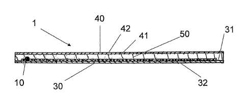
[0009] Fig. 2 is a side cross sectional view of an RFID bracelet according to
another
embodiment of the invention.
[0010] Fig. 3 is an en.larged view of an RFID bracelet according to one
embodiment
of the invention.
[0011] Fig. 4 is a side cross sectional view of an RFID bracelet in an
injection
molding apparatus prior to injection of a core layer.
[0012] Fig. 5 is a cross sectional view of an RFID bracelet in an injection
molding
apparatus after injection of a core layer.
[0013] Fig. 6 is a top cross sectional view of two RFID bracelets according to
one
embodiment of the invention.
DETAILED DESCRIPTION OF THE PREFERRED EMBODIMENTS
[0014] Embodiments of the present invention will be described below with
reference to the accompanying drawings. It should be understood that the
following
description is intended to describe exemplary embodiments of the invention,
and not
to limit the invention.
[0015] According to one embodiment of the present invention, as shown in Figs.
1
and 2, the bracelet 1 comprises a radio frequency identification ("RFID")
microprocessor 10, an antenna 20, a bottom layer 30, a top layer 40 and a core
layer
50. Further, the bracelet 1 includes extremity loops 60 for fastening the
bracelet 1 to
the wrist of a wearer.
[0016] The bottom layer 30 has a top surface 31 and.a bottom surface 32. The
bottom layer 30 is comprised of any known conventional plastic material that
does not
conduct electricity. For example, the bottom layer 30 may be comprised of PVC,
-3-
CA 02614913 2008-01-10
WO 2007/011514 PCT/US2006/025565
nylon, polyester, polypropylene, polycarbonate or teslin. The bottom surface
32 of
the bottom layer 30 is configured to display writing or any type of identify
marks.
The top surface 31 of the bottom layer 30 may be comprised of a plastic
compound
that is suitable for receiving conductive ink. As shown in Fig. 1 and
described below,
the top surface 31 of the bottom layer 30 is configured to receive and
vertically
stabilize a plurality of circuit components.
[00171 As described above, a plurality of circuit components may be attached
to the
top surface 31 of the bottom layer 30. The plurality of circuit components can
be
positioned anywhere on the top surface 31 of the bottom layer 30 as desired.
The
purpose and design functionality of the bracelet 1 will dictate the position
of the
circuit components. Functionality will also dictate what types of circuit
components
are included within the bracelet 1. For exainple purposes only, the bracelet 1
could be
populated with a battery 70, an antenna 20, and a RFID microprocessor 10.
Further,
additional circuit components may include but are not limited to LEDs,
flexible
displays and emulators.
[0018] According to one embodiment of the present invention, the top surface
31 of
the bottom layer 30 is configured to receive a RFID microprocessor 10, a
battery 70
and an antenna 20 (shown in Fig. 1). The RFID microprocessor 10 may be anyone
of
several known RFID processors. For example, a Phillips SL2 ICS20 chip may be
used as the RFID microprocessor 10. In one embodiment of the invention, a FCP2
flip-chip package is used as the RFID microprocessor 10. The RFID
microprocessor
is operably connected to a battery 70 and an antenna 20 via circuit traces 5.
[0019] As shown in Fig. 1, according to one embodiment of the invention, the
antenna 20 is deposited on the top surface 31 of the bottom layer 30. The
antenna 20
may be may be comprised of anyone of a number of materials. For example, the
antenna 20 may be comprised of solid copper wire. According to another
embodiment of the present invention, the antenna 20 is printed on the top
surface 31
of the bottom layer 30 with conductive ink. As show in Fig. 1, a disabling
tai180 is
also operably connected to the antenna 20.
-4-
CA 02614913 2008-01-10
WO 2007/011514 PCT/US2006/025565
[0020] According to one embodiment of the invention, as shown in Fig. 3, two
layers of conductive ink form circuit traces 5 on the top surface 31 of the
bottom layer
30. A first layer of conductive ink 5a forms the main loops of the antenna 20
and
encircles the disabling tai180. The first layer of conductive ink 5a also
extends
around the loops 60 of the bracelet 1. The second layer of conductive ink 5b
is
applied after the first layer of conductive ink. As shown in Fig. 3, a
dielectric coating
15 is positioned on top of the first conductive ink layer 5a where the second
layer of
conductive ink 5b intersects with the first layer of conductive ink 5a.
[0021] As shown in Fig. 2, the top layer 40 has a bottom surface 41 and a top
surface 42. The top layer 40 is comprised of any known conventional plastic
material
that does not conduct electricity. For example, the top layer 40 may be
comprised of
PVC, nylon, polyester, polypropylene, polycarbonate or teslin. The top surface
42 of
the top layer 40 is configured to display writing or any type of identify
marks. The
bottom surface 41 is configured to come into contact with a core layer 50.
10022] The core layer 50 is positioned between the top layer 40 and bottom
layer 30
and is in continuous contact with the bottom surface 41 of the top layer 40
and the top
surface 31 of the bottom layer 30. The core layer 50 is comprised of material
configured to stabilize the circuit components positioned on the top surface
31 of the
bottom layer 30 in the vertical and horizontal directions. hi addition, the
core layer 50
protects the circuit components from physical damage. The thickness of the
core
layer 50 is in the range of.005-.100 inches. Preferably, the core layer 50 is
50%
thicker than the thickness of the circuit components present on the top
surface 31 of
the bottom layer 30.
[0023] According to one embodiment of the invention, the core layer 50 is
comprised of anyone of a number of thermosetting polymeric materials. Due to
its
bonding and adhesive properties, a core thermosetting polymeric layer 50
integrates
the bottom layer 30 with the top layer 40 and the remaining components to form
a
bracelet 1.
-5-
CA 02614913 2008-01-10
WO 2007/011514 PCT/US2006/025565
[0024] The preferred thermosetting materials are polyurethane, epoxy and
unsaturated polyester polymeric materials. Specifically, polyurethanes made by
condensation reactions of isocyanate and a polyol derived from propylene oxide
or
trichlorobutylene oxide are preferred. Of the various polyesters that can be
used,
those that can be further characterized as being "ethylenic unsaturated" are
particularly preferred because of their ability to be cross linked through
their double
bonds with compatible monomers (also containing ethylene unsaturation) and
with the
materials out of which the top 40 and bottom 30 layers are made. The more
preferred
epoxy materials for use in the practice of this invention will be those made
from
epichlorohydrin and bisphenol A, or epichlorohydrin, and an aliphatic polyol
(such as
glycerol). They are particularly preferred because of their, ability to bond
with some
of the more preferred materials (e.g., polyvinyl chloride) out of which the
top 40 and
bottom 301ayers may be made.
[0025] A method for manufacturing a RFID bracelet 1 according to the present
invention will now be described.
[0026] First, a bottom layer 30 is provided. The bottom layer 30 has a top
surface
31 and a bottom surface 32. Circuit traces 5 are present on the top surface 31
of the
bottom layer 30. Next, a plurality of circuit components are placed onto the
top
surface 31 of the bottom layer 30 and electrically connected to the circuit
traces 5.
[0027] As shown in Fig. 4, the bottom layer 30 is then loaded as one complete
sheet
into an injection molding apparatus. A top surface 40 is placed into the
injection
molding apparatus and positioned such that the top layer 40 is above the top
surface
31 of the bottom layer 30. Specifically, the injection molding apparatus may
be a
reaction injection molding machine (which is often individually referred to as
"RIM").
These machines are associated with a top mold she1190 and a bottom mold
she1195
that are capable of performing cold, low pressure, forming operations on at
least one
of the sheets of polymeric material (e.g., PVC) that make up the top 40 and
bottom 30
layers. Such top and bottom mold shells 90, 95 cooperate in ways that are well
known to those skilled in the polymeric material molding arts.
-6-
CA 02614913 2008-01-10
WO 2007/011514 PCT/US2006/025565
[0028] The injection molding apparatus then injects thermosetting polymeric
material via a nozzle 100 (shown in Figs. 4 and 5) between the top layer 40
and the
bottom layer 30 forming the core layer 50 from thermosetting polymeric
material.
[0029] Cold, low pressure forming conditions generally mean forming conditions
wherein the temperature of the core layer 50 consisting of thermosetting
polymeric
material, is less than the heat distortion temperature of the top 40 and
bottom 30
layers, and the pressure is less than about 500 psi. Preferably, the cold
forming
temperatures will be at least 10 F less than the heat distortion temperature
of the top
40 and bottom 30 overlays. The heat distortion temperature of many polyvinyl
chloride (PVC) materials is about 230 degrees F.
[0030] Preferably, gates are employed that are tapered down from a relatively
wide
inflow area to a relatively narrow core region that ends at or near the
leading edge(s)
of the bracelet 1 body being formed. Most preferably, these gates will narrow
down
from a relatively wide diameter (e.g., from about 5 to about 10 mm) injection
port that
is in fluid connection with the thermosetting material-supplying runner, to a
relatively
thin diameter (e.g., 0.10 mm) gate/bracelet edge where the gate feeds the
thermosetting material into the void space which ultimately becomes the center
or
core of the finished bracelet 1. Gates that taper from an initial diameter of
about 7.0
milliineters down to a minimum diameter of about 0.13 mm will produce
especially
good results under the preferred cold, low-pressure injection conditions.
[0031] Another optional feature that can be used is the use of mold shells
that have
one or more receptacles for receiving "excess" polymeric material that may be
purposely injected into the void space between the top 40 and bottom 301ayers
in
order to expunge any air and/or other gases (e.g., those gases formed by the
exothermic chemical reactions that occur when the ingredients used to
formulate most
polymeric thermoset materials are mixed together) from said void space. These
thermoset ingredients are preferably mixed just prior to (e.g., about 30
seconds
before) their injection into the void space.
-7-
CA 02614913 2008-01-10
WO 2007/011514 PCT/US2006/025565
[0032] Once the core layer 50 has been injected, the molded structure is
removed
from the injection molding apparatus. According to one embodiment of the
invention,
several bracelets 1 are cut out of one molded sheet. Fig. 6 depicts several
bracelets 1
formed on one sheet. The finished bracelets 1 are then removed from the excess
polymeric material (e.g., by trimming) and cut to certain prescribed sizes.
The
trimming process may also remove the excess material in one cutting/trimming
operation. It also will be well appreciated by those skilled in this art that
the molding
devices used to make such bracelets 1 in commercial production operations will
most
preferably have mold shells having multiple cavities (e.g., 2, 4, 6, 8, etc.)
for making
several such bracelets 1 simultaneously.
[0033] The present invention has several advantages including a cost effective
manner to produce one or more RFID bracelets 1. The core layer 50 provides
greater
protection to circuit components inside the bracelet 1 during manufacturing
and wear
which in turn lowers production costs and raises production output. Moreover,
the
method of the present invention can be easily adapted to produce multiple
bracelets 1
at once.
[0034] The foregoing description of a preferred embodiment of the invention
has
been presented for purposes of illustration and description. It is not
intended to be
exhaustive or to limit the invention to the precise form disclosed, and
modifications
and variations are possible in light of the above teaching or may be acquired
from
practice of the invention. The embodiment was chosen and described in order to
explain the principles of the invention and as a practical application to
enable one
skilled in the art to utilize the invention in various embodiments and with
various
modification are suited to the particular use contemplated. It is intended
that the
scope of the invention be defined by the claims appended hereto and their
equivalents.
-8-