Note: Descriptions are shown in the official language in which they were submitted.
CA 02615217 2008-01-14
WO 2007/019024 PCT/US2006/028473
Grating-based Sensor Combining Label-free Binding Detection and
Fluorescence Amplification and Readout System for Sensor
PRIORITY
This application claims priority benefits under 35 U.S.C. 119 (e) to the
following
United States provisional patent applications, the entire contents of which
are incorporated by
reference herein:
(1) Serial no. 60/707,579 filed August 11, 2005
(2) Serial no. 60/713,694 filed September 2, 2005
(3) Serial no. 60/778,160 filed February 28, 2006
(4) Serial no. 60/790,207 filed April 7, 2006.
BACKGROUND
A. Field of the Invention
This invention relates generally to grating-based biochemical sensor devices
and
detection instruments for such devices. Grating-based sensors are typically
used for optical
detection of the adsorption of a biological material, such as DNA, protein,
viruses or cells,
small molecules, or chemicals, onto a surface of the device or within a volume
of the device.
The sensor of this invention has a grating structure that is constructed in a
manner for use in
two different applications: (a) label-free binding detection, and (b)
fluorescence detection, for
example wherein the sample is bound to a fluorophore or emits native
fluorescence.
B. Description of Related Art
l. Label-free detection sensors
Grating-based sensors represent a new class of optical devices that have been
enabled
by recent advances in semiconductor fabrication tools with the ability to
accurately deposit
and etch materials with precision less than 100 nm.
Several properties of photonic crystals make them ideal candidates for
application as
grating-type optical biosensors. First, the reflectance/transmittance behavior
of a photonic
crystal can be readily manipulated by the adsorption of biological material
such as proteins,
DNA, cells, virus particles, and bacteria on the crystal. Other types of
biological entities
CA 02615217 2008-01-14
WO 2007/019024 PCT/US2006/028473
which can be detected include small and smaller molecular weight molecules
(i.e., substances
of molecular weight < 1000 Daltons (Da) and between 1000 Da to 10,000 Da),
amino acids,
nucleic acids, lipids, carbohydrates, nucleic acid polymers, viral particles,
viral components
and cellular components such as but not limited to vesicles, mitochondria,
membranes,
structural features, periplasm, or any extracts thereof. These types of
materials have
demonstrated the ability to alter the optical path length of light passing
through them by
virtue of their finite dielectric permittivity. Second, the
reflected/transmitted spectra of
photonic crystals can be extremely narrow, enabling high-resolution
determination of shifts in
their optical properties due to biochemical binding while using simple
illumination and
detection apparatus. Third, photonic crystal structures can be designed to
highly localize
electromagnetic field propagation, so that a single photonic crystal surface
can be used to
support, in parallel, the measurement of a large nuniber of biochemical
binding events
without optical interference between neighboring regions within <3-5 microns.
Finally, a
wide range of materials and fabrication methods can be employed to build
practical photonic
crystal devices with high surface/volume ratios, and the capability for
concentrating the
electromagnetic field intensity in regions in contact with a biochemical test
sample. The
materials and fabrication methods can be selected to optimize high-volume
manufacturing
using plastic-based materials or high-sensitivity performance using
semiconductor materials.
Representative examples of grating-type biosensors in the prior art are
disclosed in
Cunningham, B.T., P. Li, B. Lin, and J. Pepper, Coloririzetric resonant
reflection as a direct
biochemical assay technique. Sensors and Actuators B, 2002. 81: p. 316-328;
Cunningham,
B.T., J. Qiu, P. Li, J. Pepper, and B. Hugh, A plastic colorimetNic resonant
optical biosensor
for nlultiparallel detection of label-free biochemical interactions, Sensors
and Actuators B,
2002. 85: p. 219-226; Haes, A.J. and R.P.V. Duyne, A Nanoscale Optical
Biosensor:
Sensitivity and Selectivity of an Approach Based on the Localized Surface
Plasmon
Resonance Spectroscopy of Triangular Silver Nanoparticles. Journal of the
American
Chemical Society, 2002. 124: p. 10596-10604.
The combined advantages of photonic crystal biosensors may not be exceeded by
any
other label-free biosensor technique. The development of highly sensitive,
miniature, low
cost, highly parallel biosensors and simple, miniature, and rugged readout
instrumentation will
enable biosensors to be applied in the fields of pharmaceutical discovery,
diagnostic testing,
environmental testing, and food safety in applications that have not been
economically
feasible in the past.
2
CA 02615217 2008-01-14
WO 2007/019024 PCT/US2006/028473
In order to adapt a photonic bandgap device to perform as a biosensor, some
portion
of the structure must be in contact with a test sample. Biomolecules, cells,
proteins, or other
substances are introduced to the portion of the photonic crystal and adsorbed
where the
locally confined electromagnetic field intensity is greatest. As a result, the
resonant coupling
of light into the crystal is modified, and the reflected/transmitted output
(i.e., peak
wavelength) is tuned, i.e., shifted. The amount of shift in the reflected
output is related to the
amount of substance present on the sensor. The sensors are used in conjunction
with an
illumination and detection instrument that directs light into the sensor and
captures the
reflected or transmitted light. The reflected or transmitted light is fed to a
spectrometer that
measures the shift in the peak wavelength.
The ability of photonic crystals to provide high quality factor (Q) resonant
light
coupling, high electromagnetic energy density, and tight optical confinement
can also be
exploited to produce highly sensitive biochemical sensors. Here, Q is a
measure of the
sharpness of the peak wavelength at the resonant frequency. Photonic crystal
biosensors are
designed to allow a test sample to penetrate the periodic lattice, and to tune
the resonant
optical coupling condition through modification of the surface dielectric
constant of the
crystal through the attachment of biomolecules or cells. Due to the high Q of
the resonance,
and the strong interaction of coupled electromagnetic fields with surface-
bound materials,
several of the highest sensitivity biosensor devices reported are derived from
photonic
crystals. See the Cunningham et al. papers cited previously. Such devices have
demonstrated
the capability for detecting molecules with molecular weights less than 200
Daltons (Da)
with high signal-to-noise margins, and for detecting individual cells. Because
resonantly-
coupled light within a photonic crystal can be effectively spatially confined,
a photonic
crystal surface is capable of supporting large numbers of simultaneous
biochemical assays in
an array format, where neighboring regions within -10 m of each other can be
measured
independently. See Li, P., B. Lin, J. Gerstenmaier, and B.T. Cunningham, A new
nzethod for
label-free inaaging of biomolecular interactions. Sensors and Actuators B,
2003.
There are many practical benefits for label-free biosensors based on photonic
crystal
structures. Direct detection of biochemical and cellular binding without the
use of a
fluorophore, radioligand or secondary reporter removes experimental
uncertainty induced by
the effect of the label on molecular conformation, blocking of active binding
epitopes, steric
hindrance, inaccessibility of the labeling site, or the inability to find an
appropriate label that
functions equivalently for all molecules in an experiment. Label-free
detection methods
greatly simplify the time and effort required for assay development, while
removing
3
CA 02615217 2008-01-14
WO 2007/019024 PCT/US2006/028473
experimental artifacts from quenching, shelf life, and background
fluorescence. Compared to
other label-free optical biosensors, photonic crystals are easily queried by
simply illuminating
at normal incidence with a broadband light source (such as a light bulb or
LED) and
measuring shifts in the reflected color. The simple excitation/readout scheme
enables low
cost, miniature, robust systems that are suitable for use in laboratory
instruments as well as
portable handheld systems for point-of-care medical diagnostics and
environmental
monitoring. Because the photonic crystal itself consumes no power, the devices
are easily
embedded within a variety of liquid or gas sampling systems, or deployed in
the context of an
optical network where a single illumination/detection base station can track
the status of
thousands of sensors within a building. While photonic crystal biosensors can
be fabricated
using a wide variety of materials and methods, high sensitivity structures
have been
demonstrated using plastic-based processes that can be performed on continuous
sheets of
film. Plastic-based designs and manufacturing methods will enable photonic
crystal
biosensors to be used in applications where low cost/assay is required, that
have not been
previously economically feasible for other optical biosensors.
The assignee of the present invention has developed a photonic crystal
biosensor and
associated detection instrument for label-free binding detection. The sensor
and detection
instrument are described in the patent literature; see U.S. patent application
publications U.S.
2003/0027327; 2002/0127565, 2003/0059855 and 2003/0032039. Methods for
detection of a
shift in the resonant peak wavelength are taught in U.S. Patent application
publication
2003/0077660. The biosensors described in these references include 1- and 2-
dimensional
periodic structured surfaces applied to a continuous sheet of plastic film or
substrate. The
crystal resonant wavelength is determined by measuring the peak reflectivity
at normal
incidence with a spectrometer to obtain a wavelength resolution of 0.5
picometer. The
resulting mass detection sensitivity of <1 pg/mm2 (obtained without 3-
dimensional hydrogel
surface chemistry) has not been demonstrated by any other cominercially
available biosensor.
A fundamental advantage of the biosensor devices described in the above-
referenced
patent applications is the ability to mass-manufacture with plastic materials
in continuous
processes at a 1-2 feet/minute rate. Methods of mass production of the sensors
are disclosed
in U.S. Patent application publication 2003/0017581. As shown in Figure 1, the
periodic
surface structure of a biosensor 10 is fabricated from a low refractive index
material 12 that is
overcoated with a thin film of higher refractive index material 14. The low
refractive index
material 12 is bonded to a base sheet of clear plastic material 16. The
surface structure is
replicated within a layer of cured epoxy 12 from a silicon-wafer "master" mold
(i.e. a
4
CA 02615217 2008-01-14
WO 2007/019024 PCT/US2006/028473
negative of the desired replicated structure) using a continuous-film process
on a polyester
substrate 16. The liquid epoxy 12 conforms to the shape of the master grating,
and is
subsequently cured by exposure to ultraviolet light. The cured epoxy 12
preferentially
adheres to the sheet 16, and is peeled away from the silicon wafer. Sensor
fabrication was
completed by sputter deposition of 120 nm titanium oxide (Ti02) high index of
refraction
material 14 on the cured epoxy 12 grating surface. Following titanium oxide
deposition, 3x5-
inch microplate sections are cut from the sensor sheet, and attached to the
bottoms of
bottomless 96-well and 384-well microtiter plates with epoxy.
As shown in Figure 2, the wells 20 defining the wells of the mircotiter plate
contain a
liquid sample 22. The combination of the bottomless microplate and the
biosensor structure
10 is collectively shown as biosensor apparatus 26. Using this approach,
photonic crystal
sensors are mass produced on a square-yardage basis at very low cost.
The detection instrument for the photonic crystal biosensor is simple,
inexpensive,
low power, and robust. A schematic diagram of the system is shown in Figure 2.
In order to
detect the reflected resonance, a white light source illuminates a-l mm
diameter region of
the sensor surface through a 100 micrometer diameter fiber optic 32 and a
collimating lens 34
at nominally normal incidence through the bottom of the microplate. A
detection fiber 36 is
bundled with the illumination fiber 32 for gathering reflected light for
analysis with a
spectrometer 38. A series of 8 illumination/detection heads 40 are arranged in
a linear
fashion, so that reflection spectra are gathered from all 8 wells in a
microplate column at
once. See Figure 3. The microplate + biosensor 10 sits upon a X-Y addressable
motion stage
(not shown in Figure 2) so that each column of wells in the microplate can be
addressed in
sequence. The instrument measures all 96 wells in -15 seconds, limited by the
rate of the
motion stage. Further details on the construction of the system of Figures 2
and 3 are set
forth in the published U.S. Patent Application 2003/0059855.
The descriptions and discussions below refer to the label-free technology
described
above as BIND technology. BIND is a trademark of the assignee SRU Biosystems,
Inc.
2. Fluorescence amplification sensors
U.S. Patent 6,707,561 describes a grating-based biosensing technology that is
sometimes referred to in the art as Evanescent Resonance (ER) technology. This
technology
employs a sub-micron scale grating structure to amplify a luminescence signal
(e.g.,
fluorescence, chemi-luminescence, electroluminescence, phosphorescence
signal), following
5
CA 02615217 2008-01-14
WO 2007/019024 PCT/US2006/028473
a binding event on the grating surface, where one of the bound molecules
carries a
fluorescent label. ER technology enhances the sensitivity of fluorophore based
assays
enabling binding detection at analyte concentrations significantly lower than
non-amplified
assays.
ER technology uses grating generated optical resonance to concentrate laser
light on
the grating surface where binding has taken place. In practice, a laser
scanner sweeps the
sensor at some angle of incidence (theta), typically from above the grating,
while a detector
detects fluoresced light (at longer optical wavelength) from the sensor
surface. By design,
ER grating optical properties result in nearly 100% reflection, also known as
resonance, at a
specific angle of incidence and laser wavelength (k). Confinement of the laser
light by and
within the grating structure amplifies emission from fluorophores bound within
range of the
evanescent field (typically 1-2 um). Hence, at resonance, transmitted light
intensity drops to
near zero.
As noted above, the label-free biosensors described in the above-referenced
patent
applications employ a sub-micron scale grating structure but typically with a
significantly
different grating geometry and objective as compared to gratings intended for
ER use. In
practical use, label-free and ER technologies have different requirements for
optical
characteristics near resonance. The spectral width and location of the
resonance phenomena
describes the primary difference. Resonance width refers to the full width at
half maximum,
in wavelength measure, of a resonance feature plotted as reflectance (or
transmittance) versus
wavelength (also referred to as Q factor above). Resonance width can also
refer to the width,
in degrees, of a resonance feature plotted on a curve representing reflectance
or transmittance
as a function of theta, where theta is the angle of incident light.
Optimally, a label-free grating-based sensor produces as narrow a resonance
peak as
possible, to facilitate detection of small changes in peak position indicating
low binding
events. A label-free sensor also benefits from a high grating surface area in
order to bind
more material. In current practice, one achieves higher surface area by making
the grating
deeper (though other approaches exist). Current commercial embodiments of
label-free
sensors produce a resonance near 850 mn, thus BIND label-free detection
instrumentation has
been optimized to read this wavelength.
Conversely, practical ER grating sensor designs employ a relatively broad
resonance
to ensure that resonance occurs at the fixed wavelength laser light and often
fixed angle of
incidence in the presence of physical variables such as material accumulation
on the grating
or variation in sensor manufacture. Because field strength generally decreases
with
6
CA 02615217 2008-01-14
WO 2007/019024 PCT/US2006/028473
resonance width, practical ER sensor design calls for a balance in resonance
width. By
choosing an appropriate ER resonance width, one ensures consistent
amplification across a
range of assay, instrument and sensor variables while maintaining ER signal
gain. A typical
application uses a 633 nm wavelength to excite a popular fluorescent dye,
known in the art as
Cy5. Some ER scanning instrumentation permits adjustments to incident angle to
"tune" the
resonance towards maximum laser fluorophore coupling. This practice, however,
may induce
an unacceptable source of variation without proper controls.
Known ER designs also employ more shallow grating depths than optimal label-
free designs. For example, the above-referenced '561 patent specifies the
ratio of grating
depth to "transparent layer" (i.e., high index coating layer) thickness of
less than 1 and more
preferably between 0.3 and 0.7. Optimal label-free designs employ gratings
with a similarly
defined ratio of greater than I and preferably greater than 1.5. Label-free
designs typically
define grating depth in terms of the grating line width or half period. For
example, currently
practiced commercial label-free sensors have a half period of 275 nm and a
grating depth of
approximately 275 nm, thus describing a 1:1 geometric ratio. This same sensor
design
employs a high index of refraction oxide coating on top of the grating with a
thickness of
approximately 90 nm. Thus, according to the definition in '561 patent, this
sensor has a
grating depth:oxide thickness ratio of approximately 3:1.
This disclosure reports grating-based sensor designs which are constructed in
a
manner such that it is optimized for both modes of detection (label-free and
fluorescence
amplification), in a single device. Such a grating dramatically increases the
diversity of
applications made possible by a single product.
All the previously cited art is fully incorporated by reference herein.
SUMMARY
The following embodiments and aspects thereof are described and illustrated in
conjunction with systems, tools and methods meant to be exemplary and
illustrative, not
limiting in scope. In various embodiments one or more of the above-described
problems
have been reduced or eliminated, while other embodiments are directed to other
improvements.
In one aspect, a grating-based sensor is disclosed which is optimized for
performance
in both ER mode and in a label-free detection mode. Such sensors exhibit a
broad resonance
at small angles of incidence (theta), mimicking the performance curves of a
conventional ER
grating biosensor, while also maintaining sharp resonance peak in a label-free
detection
7
CA 02615217 2008-01-14
WO 2007/019024 PCT/US2006/028473
mode. Several representative embodiments are disclosed. A first embodiment is
optimized
for ER mode in an air sample medium and with TM polarization of light
(perpendicular to the
grating). A second embodiment is disclosed which is optimized for ER mode in a
liquid
sample medium with 633 nm excitation, near normal incidence, and with TE
polarization.
Computer modeling of both embodiments indicates that each maintains sharp peak
wavelength resonance (high Q factor) in a label-free detection mode.
In one configuration, a biosensor has a periodic surface grating structure
(either in one
or two dimensions), wherein the periodic grating structure is constructed so
as to optimize
optical interrogation of the biosensor from a first light source in an
evanescent resonance
(ER) detection mode, and wherein the periodic grating structure is constructed
so as to
optimize optical interrogation of the biosensor with light from a second light
source in a
label-free detection mode. In one possible embodiment, the grating takes the
form of a two-
dimensional grating, and wherein the grating is periodic in first and second
mutually
orthogonal directions. In other embodiments, the grating is a one-dimensional
grating, with
periodicity in one direction (e.g., the X direction) but not in the second
direction.
Label-free detection use of the biosensor benefits from deeper gratings to
provide
more surface area, enabling more material attachment. More attached material
generates
more signal in the form of larger shift of the peak wavelength value. Prior ER
gratings do
not have enough surface area (depth) to render label-free sensitivity
equivalent to current
label-free grating sensors. Hence, one designs biosensors inaximize surface
area (translating
greater grating depth in this case) while maintaining a broad resonance curve
at the intended
laser excitation wavelength and low angles of incidence, preferably less than
10 degrees and
more preferably less than five degrees. Biosensors meeting ER and label-free
performance
requirements in representative one-dimensional embodiments have a grating
depth to half
period ratio of between about 0.6 and about 1.2. Grating depths of between
approximately
160 nm and approximately 210 nm are specifically contemplated. These
parameters may of
course vary to address specific sensor performance objectives, to emphasizing
ER or label-
free performance, or for example in two-dimensional gratings as disclosed
herein.
Computer simulation of grating design, in accordance with the teachings of
this
disclosure, will allow persons skilled in the art to develop other grating
designs in accordance
with this disclosure which may vary from the specifics of the first and second
embodiments
and such embodiments are offered by way of illustration and not limitation. In
a further
aspect, methods of designing dual use ER and label-free detection biosensors
are disclosed
using computer modeling techniques.
8
CA 02615217 2008-01-14
WO 2007/019024 PCT/US2006/028473
A grating-based sensor having a two-dimensional ortliogonal grating structure
suitable for both ER and label-free detection is also disclosed and may be
preferred in some
implementations. A two-dimensional grating can look like a waffle (holes), a
waffle iron
(posts), or a chessboard configuration with alternating high and low regions
in two
dimensions. Two dimensional gratings can have different periods in the X and Y
directions.
These features may have various profiles in the Z direction such as angled or
curved
sidewalls. Thus, in the case of the waffle pattern, the impressions or wells
may have a
rectangular rather than a square shape. In practice, these features will also
appear rounded in
the X and Y dimensions, i.e., will not have sharp corners. Thus, the use of
the terms
"rectangular" and "square" are intended to refer to the overall configuration
and allow for
rounded corners. This added flexibility provided by two dimensional gratings
allows one to
tune the resonance positions for both label-free detection and ER detection to
occur at
different wavelengths. This capability offers significant benefit in terms of
tuning of the ER
resonance to different excitation wavelengths while maintaining compatibility
with existing
label-free detection instrumentation. As an example, the X periodicity can
provide a broad
resonance at or near normal incidence with wavelength tuned to excite the Cy3
fluorophore
(green light) or the Cy5 fluorophore (red light), while the Y periodicity can
yield a sharp
label-free resonance between 820 and 850 nm (near infra red) similar to
currently
commercialized label-free sensors.
Two-dimensional, two-level grating structures are also disclosed as a further
embodiment of a grating-based biosensor which is structured and arranged to
have good
performance for both ER and label-free detection.
In another aspect, a method of analyzing at least one sample is disclosed
comprising
the steps of placing the at least one sample on a biosensor comprising a
substrate having a
periodic surface grating structure, wherein the periodic grating structure is
constructed and
designed for optical interrogation of the biosensor in an evanescent
reflection (ER) detection
mode as well as optimize optical interrogation of the biosensor in a label-
free detection mode.
The method further comprises the steps of illuminating the biosensor in a
readout detection
instrument with light from a light source designed for the ER detection mode
and
illuminating the biosensor with light from the light source (or possibly from
a second light
source) designed for the label-free detection mode; and analyzing light
reflection from the
biosensor. The analyzing of the sample may include detecting binding of a
component of the
sample, e.g., binding of the component of the sample to the surface of the
biosensor or
9
CA 02615217 2008-01-14
WO 2007/019024 PCT/US2006/028473
binding of second sample component (e.g., fluorophore, inhibitor or label) to
a first sample
component (e.g., protein)
In one embodiment, the readout system includes two light sources, one for BIND
(e.g., a while light source or light emitting diode) and a second light source
such as laser for
ER measurements. However, in other embodiments a single light source is
provided such as
a Xenon discharge lamp or tunable laser, with two (or more) bandpass filters
sampling the
light source to provide appropriate illumination wavelengths for the two
sensing modes.
In one possible embodiment, the sample is in an air medium, and wherein the
light
from the first light source has a polarization perpendicular to the grating
structure. In
another possible embodiment, the sample is in a liquid medium, and wherein the
light from
the first light source has a polarization parallel to the grating structure.
In one possible
embodiment, light from the first light source has a wavelength selected to
activate a
fluorophore bound to the sample. In another possible embodiment, light from
the first light
source has a wavelength selected to activate native fluorescence of the
sample. In still other
embodiments, a fraction of the sample is bound to an inhibitor, which may
include a bound
fluorophore. The sample may be, for example, a protein.
Several representative configurations of a readout and detection instrument
for the
inventive biosensor are also disclosed. In one embodiment, the readout and
detection
instrument includes a first light source adapted for obtaining ER data from
the biosensor; a
second light source adapted for obtaining label-free detection data; an
optical system
combining the light from the first and second light sources into an
illuminating beam for
illuminating the biosensor; at least one detector for detecting reflected
light from the
biosensor; and an analysis module using data from the at least one detector
and obtaining ER
and label-free data from the sample. The detector may be an imaging detector
such as a
charge-coupled device (CCD imager). Other types of detectors are also
envisioned, such as
photodetector, spectrometer, or a combination thereof, one for acquiring ER
data and one for
acquiring BIND data. In another representative configuration, the optical
system selectively
illuminates the biosensor with light from a single light source. The biosensor
may have
multiple detection sites or wells, and the instrument may include a motion
stage for
successively moving the detection sites relative to the light sources to
sequentially obtain ER
and label-free data from all the detection sites.
In sum, this disclosure describes a novel detection and quantification
platform that
combines a photonic crystal based label-free biosensor with enhanced
fluorescence
capabilities, in a single device. Alone, label-free and ER technologies have
great utility. The
CA 02615217 2008-01-14
WO 2007/019024 PCT/US2006/028473
ability to join these two detection technologies in a single biosensor creates
a powerful
approach for universal detection and selective measurement of interaction
between and
within biological materials such as cells, proteins, and small molecules. The
combined
biosensor of this disclosure is useful for detection of a broad range of
biological or chemical
sample entities. Examples of the types of samples which can be detected
include small and
smaller molecular weight molecules (i.e., substances of molecular weight <
1000 Da and
between 1000 Da to 10,000 Da), amino acids, nucleic acids, lipids,
carbohydrates, nucleic
acid polymers, viral particles, viral components and cellular components such
as but not
limited to vesicles, mitochondria, membranes, structural features, periplasm,
or any extracts
thereof.
In general, further examples of specific binding substances (samples) which
may be
detected with the biosensor of this invention include polypeptides, antigens,
polyclonal
antibodies, monoclonal antibodies, single chain antibodies (scFv), F(ab)
fragments, F(ab')2
fragments, Fv fragments, small organic molecules, cells, viruses, bacteria,
polymers, peptide
solutions, protein solutions, chemical compound library solutions, single-
stranded DNA
solutions,, double stranded DNA solutions, combinations of single and double
stranded DNA
solutions, RNA solutions and biological samples. Such biological samples could
consists of,
for example, blood, plasma, serum, gastrointestinal secretions, homogenates of
tissues or
tumors, synovial fluid, feces, saliva, sputum, cyst fluid, amniotic fluid,
cerebrospinal fluid,
peritoneal fluid, lung lavage fluid, semen, lymphatic fluid, tears and
prostatic fluid.
The biosensor described herein may be used to detect (a) binding of components
any
of these types of samples to the biosensor surface, (b) binding of the sample
to another
component of the sample, e.g., a fluorophore in the sample, and (c) binding of
the sample or
sample component to a second sample which is added to the sample. As an
example of
binding (b), the sensor surface may bind to some component of the sample, such
as for
example streptavidin-biotin or 6His, and the biosensor may be used to detect
the interaction
of the bound component of the sample with an additional grouping of components
in the
sample, such as a polymerase complex. In the latter example of binding (c), a
sample may
have a component that is attached to the surface of the biosensor and another
component
which specifically binds/attracts another component(s) from a second sample
that is placed
on the biosensor.
The sensor of this disclosure may also be used for quantification of the
amount of
material binding or interaction.
11
CA 02615217 2008-01-14
WO 2007/019024 PCT/US2006/028473
The following general examples by no means represent a complete or exclusive
listing
of novel utilities enabled by such a dual use grating-based sensor as
disclosed herein:
1. Combined, the two technologies distinguish the percentage of fluorophore
labeled
material present in a mixed sample population. The label-free signal provides
a quantitative
measure of the total mass bound to the sensor while the ER signal quantifies
the presence of
the label.
2. The combination can also increase statistical rigor in the measurement of
interactions between and within cells, proteins, and small molecules by
providing duplicate
binding signals from different sources.
3. Utilizing the Forster Resonant Energy Transfer (FRET) principle, the dual
use
sensor may enable measurement of the distance between two differentially
labeled
fluorescent molecules or two differentially labeled portions of the saine
molecule. The label-
free signal quantifies molecular density.
4. The combination of the two technologies can provide additive information.
The
label-less signal can quantify the attachment of cells with the fluorescent
signal quantifying
the amount of fluorophore labeled ligand bound to the cell. Other scenarios
are of course
possible where label-less and labeled biological entities, such as those
listed above, are
detected on the inventive biosensor.
5. The combination of the two technologies may provide a measure of the
molecular
mass by distinguishing molecular count from total bound mass.
6. The combined biosensor further permits two different independent
quantification
tests to be performed for other scenarios such as the study of inhibition
binding.
Furthermore, a more complete understanding and characterization of inhibition
binding
interactions between a protein and a substrate is possible, including the
ability to directly
quantify inhibitor ligand binding. As an additional example, the biosensor
facilitates the
study of very tight binding interactions whereby a known competitive inhibitor
with a weaker
binding affinity is employed to perturb/observe the much tighter binding
entity.
7. The combined ER and label-free biosensor is particularly useful for assays
which utilize the natural fluorescence of biological molecules (i.e., without
requiring the use
of a bound fluorescence label), to make biophysical characterization
measurements of activity
such as folding, stacking, and changes and rates of changes to these upon
interactions with
other biological molecules and small test molecules. Such characterization
measurements
could be made using a bound fluorescence label, but such bound label is not
necessarily
12
CA 02615217 2008-01-14
WO 2007/019024 PCT/US2006/028473
required, especially for biological materials having an inherent fluorescence
property. See
Charles R. Cantor and Paul R. Schimmel, parts 1-3 Biophysical Chenzisa-y - The
behavior
and study of biological rnolecules, W.H. Freeman and Company, New York,
(1980), page
443 and table 8-2 for a listing of fluorescence characteristics of protein and
nucleic acid
constituents and coenzymes, their absorption and emission spectra and
sensitivity. This
technique of using native fluorescence is especially important with nucleic
acid polymers
(DNA, RNA) (fluorescent nucleoside bases) stacking and hybridization, proteins
(fluorescent
amino acids phenylalanine, tryptophan, and tyrosine) and lipid membranes
(enhancement and
quenching effects upon incorporation of fluorophores into their different
compartmentalizations). In one embodiment, the label-free BIND feature allows
the
quantification of the amount of sample material or ligand bound thereto and
the ER feature
detects the native fluorescence and allows the sensitive tracking of the
biophysical change.
BRIEF DESCRIPTION OF THE DRAWINGS
Exemplary embodiments are illustrated in referenced figures of the drawings.
The
embodiments and figures disclosed herein are offered by way of example and not
limitation.
All questions regarding scope of the invention are to be answered by reference
to the claims.
Figure 1 is an illustration of a prior art biosensor arrangement.
Figure 2 is an illustration of a prior art biosensor and detection system for
illuminating
the biosensor and measuring shifts in the peak wavelength of reflected light
from the
biosensor.
Figure 3 is an illustration of an arrangement of 8 illumination heads that
read an entire
row of wells of a biosensor device comprising the structure of Figure 1
affixed to the bottom
of bottomless microtiter plate.
Figure 4 is a cross-section of a first embodiment of a combined ER and label-
free
detection biosensor.
Figure 5 is a cross-section of a second embodiment of a combined ER and label-
free
detection biosensor.
Figure 6 is a graph comparing transmission as a function of incident angle
theta for a
prior art ER biosensor ("NovaChip") with a computer simulation of the
embodiment of
Figure 4 when used for ER detection in a dry (air) medium environment.
13
CA 02615217 2008-01-14
WO 2007/019024 PCT/US2006/028473
Figure 7 is a graph comparing reflection as a function of wavelength for the
embodiment of Figure 4 in a label-free detection mode in an aqueous medium
environment;
the graph of Figure 7 was generated from a computer simulation of the
embodiment of Figure
4.
Figure 8 is a graph of reflection as a function of wavelength for the
embodiment of
Figure 4 in a label-free detection mode, showing a shift of the peak
wavelength value in
response to surface mass addition (e.g., by adding a sample to the biosensor).
The graph of
Figure 7 was also generated via a computer simulation of the embodiment of
Figure 4.
Figure 9 is a graph of reflection on as a function of wavelength showing the
resonance
peaks for the embodiment of Figure 5 in label-free and ER detection modes. The
graph was
generated from a computer simulation of the embodiment of Figure 5.
Figure 10 is a graph of transmission as a function of theta for the embodiment
of
Figure 5 and comparing the curve with the transmission curve of a prior art
"NovaChip"
example of an ER sensor.
Figures 11A and 11B are perspective and cross-sectional views, respectively,
of a
one-dimensional linear grating structure designed solely for ER detection,
modeled as a
rough approximation of an ER chip disclosed in a prior art article of Budach
et al.
Figures 12A and 12B are graphs of the reflection efficiency as a function of
wavelength and incidence angle, respectively, obtained when light polarized in
the X
direction is incident on the structure of Figures 1 lA and 11B.
Figures 13A-13C are plots of the X, Y and Z components of electric field
amplitude
in the XY plane corresponding to the lower surface of the structure of Figure
11A and 11B
located a Z = 110 nm, for incident wavelength 632 nm. Figures 13D-13F plot of
the X,Y and
Z components of the magnetic field amplitude in the same XY plane represented
in Figures
13A-13C for incident wavelength 632 nm.
Figures 14A -14C are plots of the X, Y and Z components of electric field
amplitude
in the XY plane corresponding to the upper surface of the structure of Figure
1 lA and 11B
located at Z = 140 nm, for incident wavelength 632 nm. Figures 14D-14F plot
the X,Y and Z
components of the magnetic field amplitude in the sanie XY plane represented
in Figures
14A-14C for incident wavelength 632 nm.
14
CA 02615217 2008-01-14
WO 2007/019024 PCT/US2006/028473
Figures 15A and 15B are perspective and cross-sectional views, respectively,
of a
two-dimensional grating design characterized by periodic holes in a grating
structure which is
optimized for BIND (label-free) detection in a water environment when
illuminated by X
polarized light and optimized for ER detection in an air environment when
illuminated by Y
polarized light.
Figures 16 and 17 are graphs of the reflection efficiency as a function of
wavelength
and incidence angle (632.5 nm), respectively, obtained when light polarized in
the Y
direction is incident on the structure of Figures 15A and 15B. These figures
demonstrate
utility in the ER mode.
Figures 18A-18C are plots of the X, Y and Z components of electric field
amplitude
in the XY plane corresponding to the lower surface of the structure of Figure
15A and 15B at
Z = 78 nm, for incident wavelength 632.5 nm. Figures 18D-18F plot the X,Y and
Z
components of the magnetic field amplitude in the same XY plane represented in
Figures
18A-18C for incident wavelength 632.5 nm.
Figures 19A -19C are plots of the X, Y and Z components of the electric field
amplitude in the XY plane corresponding to the upper surface of the structure
of Figures 15A
and 15B at Z= 433 nm for incident wavelength 632.5 nm. Figures 19D-19F are
plots of X,Y
and Z components of the magnetic field amplitude in the 'same XY plane
represented in
Figures 19A-19C for incident wavelength 632 nm.
Figure 19G is a graph of reflection efficiency as a function of wavelength for
the
embodiment of Figure 15 obtained when illuminated by light polarized 'in the X
direction.
This resonance peak is used for label-free detection.
Figures 20A and 20B show perspective and cross-sectional views, respectively,
of a
two-dimensional grating design characterized by periodic posts in a grating
structure which is
optimized in one direction for BIND (label-free) detection in a water
environment when
illuminated by X polarized light and optimized for ER detection in an air
environment when
illuminated by Y polarized light.
Figures 21 A and 21 B graph the reflection efficiency as a function of
wavelength and
incidence angle (633 nm wavelength), respectively, when light polarized in the
X direction is
incident on the structure of Figures 20A and 20B. The figures demonstrate
utility in the ER
mode.
CA 02615217 2008-01-14
WO 2007/019024 PCT/US2006/028473
Figures 22A-22C are plots of the X, Y and Z components of electric field
amplitude
in the XY plane corresponding to the lower surface of the structure of Figure
20A and 20B at
Z = 70 nm, for incident wavelength 633 nm. Figures 22D-22F plot the X, Y and Z
components of the magnetic field amplitude in the same XY plane represented in
Figures
22A-22C for incident wavelength 633 nm.
Figures 23A -23C plot the X, Y and Z components of the electric field
amplitude
corresponding to the upper surface of the structure of Figure 20A and 20B at
Z= 430 nm for
incident wavelength 633 nm. Figures 23D-23F plot the X, Y and Z components of
the
magnetic field amplitude in the same XY plane represented by Figures 23A-C for
incident
wavelength 632 nm.
Figure 24 is a graph of reflection efficiency as a function of wavelength for
the
embodiment of Figure 20 obtained when illuminated by light polarized in the X
direction.
This resonance peak is used for label-free detection.
Figure 25 is a schematic drawing of an imaging readout system for a combined
ER
and label-free grating-based sensor.
Figure 26 is a schematic illustration of a second readout system for a
combined ER
and label-free grating-based sensor.
Figure 27 is a more detailed illustration of the embodiment of Figure 26.
Figures 28A-C are three views of a unit cell showing a two-level, two-
dimensional
grating structure for yet another embodiment of a combined ER and label-free
sensor.
Figure 29 is a graph of the reflection spectrum (relative intensity as a
function of
reflected light wavelength) obtained using a computer simulation of the
structure of Figure
28A-C.
Figure 30 is a cross-sectional view of a combined ER and BIND grating-based
sensor
in which an intermediate Si02 layer is added between the UV-cured plastic
grating layer and
the high index of refraction layer forming the upper surface of the sensor.
Figure 31 is an image of a microarray of spots deposited on a grating-based
sensor
(which may or may not be optimized for both ER and BIND measurements).
Figure 32 is a graph of a peak shift for one of the spots of Figure 31 due to'
presence
of a DNA sample being placed on the sensor.
16
CA 02615217 2008-01-14
WO 2007/019024 PCT/US2006/028473
Figure 33 is an illustration of a row of spots showing the shift in peak
wavelength
value in nanometers (which is quantitatively related to the amount of DNA in
the spot) as a
function of position and showing a missing spot (dark location in the row of
spots), the
missing spot indicated by the low region in the graph.
DETAILED DESCRIPTION
Grating-based biosensors are disclosed which have a periodic grating
construction
which is optimized and useful for both ER detection, either in a liquid or dry
environment,
and for label-free detection. A readout system adapted for use with the
biosensors is also
described. Methods of testing a sample with the inventive biosensors are also
described.
First Embodiment
Figure 4 is a schematic cross-sectional illustration of a first embodiment of
a one-
dimensional sensor having a grating structure 100 that is expected to meet
commercial
requirements for both ER and label-free applications of a grating-based
sensor. Figure 4
shows one period of a grating structure 100 in one dimension or direction. The
diinensions
are not to scale in Figure 4.
The grating 100 of Figure 4 is superimposed and bonded to a base sheet of
clear
material such as Polyethylene Terepthalate (PET) or other plastic, glass or
other material (not
shown).
The grating structure consists of a periodically repeating material 102 which
preferably comprises a UV-cured material, e.g., epoxy, applied with the aid of
a grating
master wafer (not shown) to replicate the grating pattern onto the base sheet
of PET material
located below the layer "substrate." The UV cured material 102 is applied to a
substrate
sheet such as PET. Substrate materials can also include polycarbonate or cyclo-
olefin
polymers such as Zeanor . Other means of producing the structured layer 102
include
thermally stamping directly into a polymer substrate. The middle material 104
represents a
sputtered oxide coating with high refractive index (e.g. Ti02 or Ta205). The
upper most
material 106 represents a medium for a sample, which is normally either a
water-based
buffer, for label-free detection mode, or air, for ER mode. The structure has
the periodicity,
layer structure, and horizontal transition points as shown in the Figure. The
specifics of the
17
CA 02615217 2008-01-14
WO 2007/019024 PCT/US2006/028473
design of course may change while still providing good performance for both
label-free
detection and ER detection.
The design of Figure 4 was developed and its performance modeled with the aid
of a
computer and a software program GSolver (Grating Solver Development Co., Allen
Texas,
www.gsolver.com). The various geometrical dimensions and parameters; spacing,
well
depth, materials, and index of refraction data associated with the materials
allows the design
to be studied on a computer and simulations run to predict the Transmission v.
Theta curve
and reflection as a function of wavelength curve. Such simulations can be run
in situations
where the sample is dry and when the sample is suspended in water or other
fluid medium
with known index of refraction. Such simulations allow the designer to
optimize, i.e.,
change, the various design parameters (thicknesses, transitions, period, etc.)
to satisfy the
requirements for both ER and label-free detection.
ER technology heretofore employs a resonance mode induced by incident light
with a
polarization parallel to the grating, defined here as TE mode or polarization.
Label-free
detection technology typically employs a resonance mode induced by incident
light with
polarization perpendicular to the grating, defined here as the TM mode or
polarization. This
mode produces the narrowest resonance when the sample is suspended in a liquid
medium.
In the first embodiment of Figure 4, a grating biosensor design is described
which
utilizes TM polarization for both label-free detection of a sample suspended
in liquid and ER
detection in an air (dry) environment. Changing the medium above the grating
from water to
air results in a change in resonance characteristics from those useful for
label-free detection
to those useful for ER amplification of dyes responding to 633 nm excitation.
The design of
Figure 4 is not specifically optimized to ER detection in a water mode and may
not even
work acceptably for ER in a water mode. However, many ER detection assays are
run in an
air environment and so the design of Figure 4 has much utility for ER
detection.
Figure 6 is a graph that compares Transmission v. Theta data for a prior art
ER device
(NovaChip, Novartis AG) with a computer simulation or model of the first
design of Figure 4
("Combind 400 Air"). NovaChip data is disclosed in Budach et al., Generation
of
Transducers for Fluorescence-Based Microarrays with Enhanced Sensitivity and
Their
Application to Gene Expression Profiling, Analytical Chemistry (2003) and in
Neuschafer et
al., Evanescent resonator chips: a universal platform with superior
sensitivity for
fluorescence-based microarrays, Biosensors and Bioelectronics 18 (2003) 489-
497. The
curves 110 and 112 have a similar shape suggesting the simulated device
(ComBIND 400)
would function equivalently to the ER device. The NovaChip TE resonance occurs
at - 2
18
CA 02615217 2008-01-14
WO 2007/019024 PCT/US2006/028473
degrees from normal incidence. The first design of Figure 4 produces TE
resonance at -3
degrees, which is considered only a minor difference given that one can adjust
the angle of
incident light (see the discussion of the readout and detection instrument for
the sensor later
in this disclosure).
The graph of Figure 7 plots simulated reflection vs. wavelength for the
ComBind 400
design (Figure 4). The broad reflection peak centered around 628 nm
corresponds to the ER-
air mode resonance occurring at - 3 degrees in the Transmission v. Theta curve
above. The
narrow peak, labeled "water", serves for the label-free mode of detection.
Note the extreme
sharpness of the peak 114. This suggests that the design of Figure 4 would
work well for
label-free detection in a water environment.
During label-free mode detection, biological molecules adhere to the Ti02
coating and
effectively increase the optical thickness of that material. This results in a
shift in the peak
wavelength value (PWV) of the resonance. A larger PWV shift for a fixed amount
of material
represents higher detection sensitivity. When comparing grating designs in a
computer
simulation, the simulation of additional biological material can be modeled by
incrementing
the thickness of the Ti02 layer rather than adding a hypothetical biological
layer. This
method has proven effective in other grating design exercises.
Figure 8 is a graph that plots the peak wavelength value in a water
environment
before and after the addition of a certain amount of simulated mass (simulated
by increasing
the thickness of the Ti02 layer 104 of Figure 4). The peak position shifts to
higher
wavelength, as is expected in label-free biosensor operation. The ratio of
wavelength shift to
simulated mass is equivalent to that of the commercialized biosensors of the
applicant's
assignee. Hence, the grating of Figure 4 is expected to yield equivalent label-
free
performance to the current label-free biosensor gratings.
To summarize, simulations predict dual-use capabilities for the grating design
disclosed in Figure 4. When dry, it can amplify fluorescent binding signals
according to the
technology known as evanescent resonance (ER). When wet, the grating performs
as well as
a label-free detector according to the technology known as guided mode
resonance detection
or commercially as BIND (trademark of SRU Biosystems, Inc.), available from
the
applicants' assignee SRU Biosystems, Inc.
Second Embodiment
Figure 5 is a cross-section of a second embodiment, showing one period of the
grating
structure in one dimension and the structure of the of the UV cured layer 102,
the high index
19
CA 02615217 2008-01-14
WO 2007/019024 PCT/US2006/028473
of refraction layer 104, and the sample medium 106. The dimensions and
transition points
are as shown in the drawing. The drawing is not to scale.
The design of Figure 5 differs from that of Figure 4 is several respects:
a) It has a shorter grating period.
b) It has narrower grating troughs or recesses. The "duty cycle" (percentage
of the
grating at the upper level in a unit cell) is 88 % in Figure 5 (0 to 0.85 and
0.97 to 1.0).
Narrow troughs with duty cycles of between 70 and 95 % are exemplary of the
narrow trough
embodiments. The narrow troughs generally give better label-free detection
results. The
narrow trough feature narrows the TE resonance peak, thus indicating increased
field
strength. While practical use of the ER effect requires a sufficiently broad
resonance, a
resonance with excessive width will have insufficient field strength to
produce useful
fluorescence signal amplification
c) It has a 1:1 ratio of grating depth to half period.
The design of Figure 5 exemplifies a one-dimensional sensor that enables both
label-
free and ER operation in a water (or buffer) environment. This contrasts with
the design of
Figure 4, which is designed for ER operation in air and label-free operation
in water. The
graph of Figure 9 shows the ER (TE polarization) and comparatively narrow
label-free (TM
polarization) spectral resonance characteristics in a water environment for
the design of
Figure 5. The graph was generated from a computer simulation of the embodiment
of Figure
5. The graph of Figure 10 compares the TE angular resonance, using 633 nm
excitation, of
the Figure 5 design ("ComBIND 370") as compared to a prior art NovaChip. In
this case,
the simulated transmission minimum 116 occurs below five degrees angle of
incidence, close
to that of the existing NovaChip ER device. The incident angle, period,
excitation
wavelength, high index of refraction material thickness, grating duty cycle,
and grating depth
all interrelate. Excitation wavelengths for commercial fluorophores are known
and can be
looked up. Angles of incidence of less than 25 degrees should be acceptable
but angles near
normal (Theta close to zero) are preferred. With angle and wavelength confined
to narrow
ranges, designing a grating with functional and commercially useful ER and
label-free
performance one must determine a grating period, duty cycle, depth and high
index of
refraction material thickness that result in high PWV shift in response to
mass attachment, for
label-free use, and high surface field at the excitation wavelength of the
specified fluorophore
or dye for ER mode. Additionally, the design must produce a label-free
resonance with
CA 02615217 2008-01-14
WO 2007/019024 PCT/US2006/028473
spectral width as narrow as possible while maintaining an ER resonance with
angular width
enough to yield a practical parameter window for measurement. The design may
incorporate
performance trade-offs. For exainple, optimization of ER performance engages a
trade-off
between field strength, which yields signal amplification, and tolerance for
sensor, instrument
and assay variables. Narrower ER resonance generally indicates higher field
strength while
broader ER resonance provides increased measurement tolerance. Typically,
label-free and
ER performance optimization involves another trade-off between grating depth,
which
enhances label-free performance, and ER resonance width. For example, in the
case of the
design of Figure 5, increasing the grating depth widens the TE/ER resonance
beyond
optimum. Increasing the duty cycle (narrowing the troughs) compensates,
narrowing the
resonance back towards optimum, and thus maintaining field ER strength.
Thus, one preferred approach to finding a dual use granting structure for both
ER and
label-free detection modes involves finding a grating with depth to half
period ratio
approximately in the range of 0.6 to 1.2 or more that also yields a broad
angular resonance in
either TM mode in an air environment, TE mode in air environment, or TE mode
in a water
environment, at the excitation wavelength of interest (e.g., 633 nm) and a
resonance angle
less than 25 degrees. This broad resonance preferably has a width between 1
degree and 10
degrees or, in terms of spectral width, between 5 nm and 30 nm. Such design
efforts can be
readily implemented in a computer, e.g., using the Gsolver software. More
directly, one can
comparatively model field strength at the grating surface using a software
such as R-Soft,
available from RSoft Design Group, www.rsoftdesigngroup.com.
Grating depths in the range of 100 to 600 nm and grating periods in the range
of 300
to 600 nm are considered exemplary.
Persons skilled in the art having the benefit of this disclosure will be able
to model
potential grating designs on a computer and arrive at suitable designs in
accordance with this
invention.
Two-dimensional aratings
The possibility of a two-dimensional (2-D) grating structure, suitable for
both ER and
label-free detection, is also contemplated and may be preferred. A two-
dimensional grating
can look like a waffle (holes), a waffle iron (posts), or a chessboard
configuration with
alternating high and low regions in two dimensions. Two-dimensional gratings
can have
different periods in the X and Y directions. These features may have various
profiles in the Z
21
CA 02615217 2008-01-14
WO 2007/019024 PCT/US2006/028473
direction such as angled or curved sidewalls. Thus, in the case of the waffle
pattern, the
impressions or wells may have a rectangular rather than a square shape. This
added
flexibility allows one to tune the resonance positions for both label-free
detection and ER
detection to occur at different wavelengths. This flexibility offers
significant benefit in terms
of tuning the ER resonance to different excitation wavelengths while
maintaining
compatibility with existing label-free detection instrumentation. As an
example, the X
periodicity can provide a resonance at or near normal incidence with
wavelength tuned to
excite the CY3 fluorophore (green light) or the CY5 fluorophore (red light),
while the Y
periodicity can yield a resonance fixed between 820 and 850 nm (in the near
infra red).
The examples of 2-D biosensor structures described herein were developed using
computer simulations and Rigorous Coupled Wave Analysis (RCWA) with a
commercially
available software package (RSoft). The computer simulations enable the device
designer to
vary the physical parameters of the device (refractive index, thickness,
width, height,
structural shape) to determine: 1) the electromagnetic field distribution
within and around the
device, 2) the reflectance or transmittance behavior as a function of incident
angle of light
and wavelength of light, and 3) how the reflected (or transmitted) spectruni
is changed by the
attachment of biomolecular material to the surface of the biosensor.
The specific 2-D embodiments described herein are optimized for combined
detection
by BIND and ER methods in a single device where the sensor contacts water
during the
BIND measurement and air during the ER measurement. Any combination of dry and
wet
for BIND and ER may be similarly optimized (e.g., measure both BIND and ER in
a wet
mode).
To more fully appreciate the advantages provided by the combined ER and BIND
(label-free) two-dimensional device, a discussion will initially be presented
in conjunction
with Figures 11-14 of a linear (one-dimensional) structure optimized for ER
only.
Simulations were first performed on the ER-only structure. The structure
corresponds
approximately to a prior art ER chip published by Budach et al., Generation of
Transducers
for Fluorescence-Based Microarrays with Enhanced Sensitivity and Their
Application for
Gene Expression Profiling, Anal Chem 2003, 75, 2571-2577. (Note: The Budach et
al.
grating is a linear grating and so is a 1-D structure as that term is used
herein. The thinner
TiOz high index of refraction of material of Figure 11A-11B as compared to the
thicker
Ta205 layer described by Budach et al, paper achieves a device of equivalent
optical
"thickness" by taking into account the different indices of refraction of the
two materials. The
22
CA 02615217 2008-01-14
WO 2007/019024 PCT/US2006/028473
modeling of Figure 11A-11B is not meant to exactly replicate the Budach et al.
device, but
rather to approximate it.)
The simulations were done to determine the electromagnetic field distribution
as well
as reflection as a function of angle and wavelength for a representative
device for ER
enhancement of Cy5 dye. In particular, Figures 11A and I1B are perspective and
cross-
sectional views, respectively, of a one dimensional linear grating structure
designed solely for
ER detection. As shown, the structure has a linear grating profile consisting
of a 30 nm
raised ridge 201 and a I 10 nm Ti02 layer 203 covering the raised ridge 201.
The periodicity
is in the Y-direction (ridge 201 repeating every 356 nm.
Figures 12A and 12B graphs the reflection efficiency as a function of
wavelength and
incidence angle, respectively, of the structure of Figures IlA and 11B, as
determined by
RCWA. Note that at normal incidence, the peak wavelength (632 nm in Figure
12A)
corresponds to the excitation wavelength of Cy5, and that there is a broad
range of angles
(Figure 12B) with high reflection efficiency of the 632 nm wavelength when the
incident
light is rotated at an angle, theta, in a parallel direction with respect to
the grating line or
ridge 201.
Figures 13A-13C are plots of the X, Y and Z components of electric field
intensity in
the XY plane corresponding to the lower surface of the structure of Figure IOA
and lOB
located a Z = 110 nm, for incident wavelength at 632 nm. Figures 13D-13F plot
of the X, Y
and Z components of the magnetic field intensity in the same XY plane
represented in
Figures 13A-13C for incident wavelength at 632 nm.
The plots of Figure 13 show the strength of the three components of the
electric field
vector (Ex, Ey, and Ez) and the magnetic field vector (Hx, Hy, and Hz) as a
function of XY
position on the lower exposed surface of the device. The upper exposed portion
of the
structure 200 is shaded here because the upper surface lies in a different
horizontal plane than
the lower surface. In the computer simulation, the sensor is illuminated with
a light source
having a I V/m magnitude electric field and a lA/m magnetic field at the
resonance
wavelength. Hence, field strength values greater than 1 represent
concentration of field
intensity at the sensor surface resulting from resonance. The power of the
electromagnetic
field is calculated by the cross product of E and H field components. The
field power, at a
given location on the structure's surface, specifies the energy available to
excite fluorophores
bound to the structure's surface. Higher power will, in theory, result in
higher fluorescence
emission. The plots show that the electric and magnetic fields, and thus the
power, do not
distribute evenly over the structure's surface, but instead locations exist
with higher than
23
CA 02615217 2008-01-14
WO 2007/019024 PCT/US2006/028473
average power (areas in red and orange in a color version of the drawing
indicated at 202)
and with lower than average power (areas in a color version of the drawing,
areas in in violet
or blue, indicated at 204). ,
Figures 14A -14C are plots of the X, Y and Z components of electric field
intensity in
the XY plane corresponding to the upper surface of the structure of Figure 11A
and 11B
located at Z = 140 nm, for incident wavelength 632 nm. Figures 14D-14F plot
the X, Y and
Z components of the magnetic field intensity in the same XY plane represented
in Figures
14A-14C for incident wavelength 632 nm.
These plots (Figure 14) show the strength of the three components of the
electric field
vector (Ex, Ey, and Ez) and the magnetic field vector (Hx, Hy, and Hz) as a
function of XY
position on the upper exposed surface of the device. The lower exposed portion
of the
structure is shaded here as indicated at 200 because the upper surface lies in
a different
horizontal plane than the lower surface. As with the plots of Figure 13, in
the simulation the
sensor is illuminated with a light source having 1 V/m electric field, lA/m
magnetic field
amplitudes at the resonant wavelength. Hence, field strength values greater
than 1 represent
the concentration of field intensity at the sensor surface, resulting from
resonance. The cross
products of E and H field components, as before, represent the instantaneous
power
distribution, at the resonant wavelength, available for fluorophore
excitation.
A. Holes embodiment example
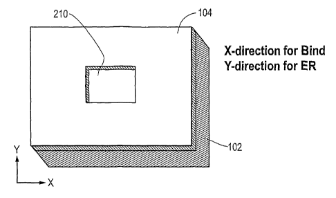
Now, a specific example of a 2D "holes" embodiment of a combined biosensor
will
be described in conjunction with Figures 15-19. The biosensor is constructed
in two
dimensions so as to be optimized for both ER and label-free (BIND) detection
using a single
device.
Figures 15A and 15B provide perspective and cross-sectional views,
respectively, of
a unit cell for a two-dimensional grating design characterized by periodic
holes 210 in a
grating structure. The grating design optimizes for water mode BIND (label-
free) detection
and air mode ER detection. The device includes an upper Ti02 layer 104 of 78
nm thickness
and a lower substrate 102 layer of UV-cured material having a grating pattern
as shown
applied to a base substrate sheet.
The two-dimensional unit cell shown in Figures 15A and 15B differentiates from
the
one-dimensional linear grating design of Figures 11A and 11B. The structure of
Figure 15A
24
CA 02615217 2008-01-14
WO 2007/019024 PCT/US2006/028473
and 15B is designed in such a way that incident light polarized perpendicular
to the X-axis, as
shown, produces a BIND signal, incident light polarized perpendicular to the Y-
axis enables
ER measurement. Using this design method, the BIND and ER resonant wavelengths
(at a
particular angle of incidence - preferably near normal incidence) may be
chosen
independently, and so the respective BIND and ER resonant wavelengths may
occur at very
different values. The combined BIND/ER structure described in this embodiment
is
optimized to provide a BIND resonance in the near infrared (-800-900nm)
wavelength
region, while providing an ER resonance at 632.5nm for excitation of the Cy5
fluorophore.
In this example, the design assumes a water environment over the sensor during
BIND
measurement and an air environment over the sensor during ER measurement. The
differing
wavelength requirements for ER and BIND engender selection of a unit cell with
a
rectangular "hole" (210). Thus, the unit cell may have differing dimensions in
the X and Y
directions. For example, the period in the X direction is 550 nm for the BIND
wavelength,
but is 432 nm in the Y direction as required for the lower wavelength ER
resonance. The
fabrication process dictates that the high refractive index dielectric
thickness will be the same
in the X and Y directions. For fabrication simplicity, the design also has
uniform grating
depth. The fabrication process will also result in rounding of the hole
corners, however the
principal function of the design remains unchanged. One skilled in the art
will appreciate that
when a computer is used to generate and test a design such as shown in Figure
15A and 15B,
the designer can change the specific dimensions of the unit cell, grating
depth, and coating
layers and run simulations of field intensity, peak wavelength, reflectance as
a function of
theta, and other tests and may select other dimensions while still achieving
acceptable results.
Thus, the example of Figure 15A and 1 SB is meant to be an illustrative
embodiment and not
limiting in scope.
Figures 16 and 17 are graphs of the reflection efficiency as a function of
wavelength
and incidence angle, respectively, for the structures disclosed in Figures 15A
and 15B when
illuminated with light polarized along the Y axis. These figures, generated by
RCWA,
represent operation in an ER mode. Figure 17 shows that, at the resonant
wavelength, the
reflected intensity as a function of incident angle observes the acceptance
angle for light that
will induce a significant ER effect. In physical measurements, the double peak
and dip
between the peaks in the plot of Figure 16 may not resolve.
In a similar manner to the ID example above, RCWA calculations may be used to
determine the spatial distribution of the amplitude of the electric field
magnitude components
(Ex, Ey, and Ez) and the magnetic field components (Hx, Hy, Hz) at the ER
resonant
CA 02615217 2008-01-14
WO 2007/019024 PCT/US2006/028473
wavelength for the structure illustrated in Figures 15A and 15B. Figures 18A-
18C plots the
X, Y and Z components of electric field intensity in the XY plane
corresponding to the lower
surface of the structure of Figure 15A and 15B at Z= 78 nm, for incident
wavelength 632.5
nm. Figures 18D-18F plot the X,Y and Z components of the magnetic field
intensity in the
same XY plane represented in Figures 18A-18C for incident wavelength 632.5 nm.
These
field amplitude distributions are shown for the lower TiOz surface inside the
hole for a single
unit cell that repeats in both the X and Y directions. As before, the cross
product of the E and
H field components describes the instantaneous power density distribution
responsible for
fluorescent excitation at the lower surface. A 1 V/m electric field, 1 A/m
magnetic field
plane wave at the resonant wavelength is used as the illumination source.
Similarly, the electromagnetic field distributions may be computed for the
upper Ti02
surface of the unit 'cell. Figures 19A -1 9C plots the X, Y and Z components
of the electric
field amplitude in the XY plane corresponding to the upper surface of the
structure of Figures
15A and 15B at Z= 433 nm for incident wavelength 632.5 nm. Figures 19D-19F
plot of X,Y
and Z components of the magnetic field amplitude in the same XY plane
represented in
Figures 19A-19C for incident wavelength 632 nm. Note that the maximum
amplitude of
each field component, as indicated by the plot legend, is substantially higher
than those of the
prior art design indicating that higher power density may be obtained at the
surface of this
device. In particular, note that a substantial Ez component has appeared in
contrast to the Ez
amplitude of the 1 D prior design. Figure 19G plots reflection efficiency as a
function of wavelength modeled using
incident illumination polarized parallel to the X axis. Light with X axis
polarization,
incident on the design represented by Figure 15, generates a resonance useful
for label-free
detection, with a width of approximately 12.5 nm and a maximum near 830 nm.
The
simulation can also predict the bulk refractive index shift coefficient,
defined as delta
(PWV)/delta(n), where delta (PWV) is the shift in the peak wavelength value
induced by a
refractive index change of delta (n) in the enviroriment above the sensor.
This quantity
indicates the sensitivity of the sensor to binding of a sample to the grating
surface. The
"Hole" design described by Figures 15A and 15B has a predicted bulk shift
coefficient of
200, indicating that the structure will provide sensitive label-free
performance.
B. Posts embodiment example
26
CA 02615217 2008-01-14
WO 2007/019024 PCT/US2006/028473
A 2-dimensional grating structure using a repeating unit cell characterized by
a post
will now be described with reference to Figures 20-24.
Figures 20A and 20B are perspective and cross-sectional views, respectively,
of a unit
cell of 2-dimensional grating design characterized by periodic posts 220
formed in the sensor
surface. Each unit cell has one post 220. The posts 220 are raised projections
in a substrate
material 102 (e.g., UV cured polymer) which is applied to a base sheet (not
shown). A high
index of refraction (e.g., Ti02) coating is applied to the projections and
substrate as shown in
the Figures. The structure is optimized for BIND (label-free) detection in a
water
environment using light polarized in the X direction and optimized for ER
detection in an air
mode, using light polarized in the Y direction.
The design of Figure 20 was studied by RCWA computer simulation. While the
previous structure unit cell of Figure 15 contained a "hole" region surrounded
by regions at a
higher plane in the z-direction, the grating structure of Figure 20 contains a
central "post"
region, surrounded by regions at a lower plane in the z-direction. As before,
the design of
Figure 20 represents a BIND/ER combined structure that is optimized to provide
a BIND
resonance in the near infrared (-800-900 nm) wavelength region, while
providing an ER at
632 nm for excitation of the Cy5 fluorophore. In this example, the design
again assumes a
water environment over the sensor during BIND measurement and an air
environment over
the sensor during ER measurement. These differing wavelength requirements for
ER and
BIND, engender selection of a rectangular "post" unit cell. Thus, the unit
cell may have
differing dimensions in the X and Y directions. For example, the period in the
X direction is
530 nm for the BIND wavelength, but is 414 nm in the Y direction as required
for the lower
wavelength ER resonance. The fabrication process again dictates that the high
refractive
index dielectric thickness will be the same in the X and Y directions. For
fabrication
simplicity, the design also has uniform grating depth. The fabrication process
will also result
in rounding of the post corners, however the principal function of the design
remains
unchanged. The example of Figure 20 is meant as an illustrative example not
limiting in
scope. The specific dimensions can of course vary.
Figures 21A and 21B graph the reflection efficiency as a function of
wavelength and
incidence angle, respectively, for the structures represented by Figures 20A
and 20B when
illuminated with light polarized along the Y axis. These figures, generated by
RCWA,
represent operation in an ER mode. Figure 21A shows a resonance peak maximum
reflection at 633 nm and Figure 21B shows a resonance across a range of
incident angles
when illuminated at 633 nm.
27
CA 02615217 2008-01-14
WO 2007/019024 PCT/US2006/028473
The RCWA computer simulations may be used to determine the spatial
distribution of
the amplitude of the electric field components (Ex, Ey, and Ez) and the
magnetic field
components (Hx, Hy, Hz) at the ER resonant wavelength. Figures 22A-22C plot
the X, Y
and Z components of electric field amplitude in the XY plane corresponding to
the lower
surface of the structure of Figure 20A and 20B at Z = 70 nm, for incident
wavelength 633
nm. Figures 22D-22F plot the X,Y and Z components of the magnetic field
amplitude in the
same XY plane represented in Figures 22A-22C for incident wavelength 633 nm.
As shown
in Figure 22, the field amplitude distributions are shown for the lower
surfaces surrounding
the posts for a single unit cell that repeats in the X and Y directions. As
before, the cross
product of the E and H field components describes the instantaneous power
density
distribution responsible for fluorescent excitation at the lower surface. A I
V/m electric field,
1 A/m magnetic field plane wave at the resonant wavelength again serves as the
illumination
source. ,
Similarly, the electromagnetic field distributions may be computed for the
upper Ti02
surfaces of the unit cell. Figures 23A-23C plot the X, Y and Z components of
the electric
field amplitude corresponding to the upper surface of the structure of Figure
20A and 20B at
Z= 430 nm for incident wavelength 633 nm. Figures 23D-23F plot the X,Y and Z
components of the magnetic field amplitude in the same XY plane represented by
Figures
23A-C for incident wavelength 632 nm. Note that the maximum magnitude of the
fields is
again substantially higher than the prior art design (Figure 10) for each of
the field
components, indicating that potentially higher power density niay be obtained
at the surface
of this device.
Figure 24 plots reflection efficiency modeled using incident illumination
polarized
parallel to the X axis. Light with X-axis polarization, incident on the deign
represented by
Figure 15, generates a resonance useful for label-free detection, with a width
of
approximately 8 nm and reflectance maximum near 805 nm. The simulations
produce a shift '
coefficient (explained above) of 90. The embodiment of Figure 20 is also
expected to
provide sensitive label-free performance, though probably lower than the
embodiment of
Figure 15. Comparison of amplitude values and shift coefficients between the
two 2D
designs suggests that further optimization of the grating structure could
emphasize the
performance of one detection mode as a tradeoff for reduced performance in the
other
detection mode.
28
CA 02615217 2008-01-14
WO 2007/019024 PCT/US2006/028473
The amount of amplification for ER detection relates to the power transferred
from
the device structure to a distribution of fluorophores on the sensor surface
within at the
excitation wavelength range of the fluorophore. The power density distribution
of the sensor
surface at the resonant wavelength, provided that the resonant wavelength
falls within the
excitation wavelength range, therefore provides a means for comparing the
sensitivity of
different ER device designs. One can define the cross product E(max) X H (max)
as a field
power or "magnification factor". While a more thorough analysis of the
intensity distribution
of the evanescent field from the tops, bottoms, and sides of the structure,
and a detailed
integration of power density to account for differences between higher and
lower power
regions would provide a more exact prediction of whether one device will
function more
effectively than another, the product of the maximum amplitude of an E
component with an
orthogonal H component provides a very simple, rough way of comparing designs.
Using
RCWA analysis for the exposed upper and lower planes of the devices, the E X H
magnification factor for the prior art design of Figure 11A and 11B is 144.
Conversely, for
the "holes" unit cell design of Figure 15A and 15B, the E X H magnification
factor is 6217,
while for the "posts" design of Figures 20A and 20B, the E X H magnification
factor is 5180.
Based on this rough analysis, the ER aspects of the 2D grating designs of
Figures 15 and 20
appear to provide the potential for higher sensitivity ER performance than the
linear grating
design of Figure 10. Moreover, the designs of Figures 15 and 20 are expected,
based on the
computer simulations, to provide excellent sensitivity for label-free
detection, as explained
above. Therefore, useful combined ER and label-free detection in a single
device is achieved
in the above-described 2D grating embodiments.
C. Two-level, 2-D gratings
Figures 28A-C are three perspective views of yet another embodiment of a unit
cell
500 for a biosensor grating structure constructed and designed for a combined
ER and label-
free (BIND) detection. In order to appreciate some of the features of this
structure, it will be
useful to recapitulate on the design aspects pertinent to evanescent resonance
(ER) and label-
free (BIND) sensors. Such sensors differ in three basic design aspects,
namely: resonance
wavelength, resonance width, and grating depth.
Resonance Wavelength
The ER sensor prefers resonance to occur in within a few (-+/-2) nm of the
excitation
wavelength. Given that the excitation light generally comes from a laser and
has very narrow
bandwidth, this requirement places high specificity on the wavelength location
of the ER
29
CA 02615217 2008-01-14
WO 2007/019024 PCT/US2006/028473
resonance. The BIND mode of operation does not have this limitation and may
benefit from a
resonance at another wavelength e.g. outside ambient lighting wavelength range
or to
separate the BIND signal spectrally from the ER excitation source thereby
eliminating
potential overlapping detection conflicts.
Resonance Width
The ER sensor must have a resonance wide enough for it to overlap the
excitation
wavelength in the presence of variables such as biological coating thickness
and illumination
numerical aperture. In practice, the ER resonance should not have a fu11 width
at half
maximum (FWHM) less than about 5 nm, and more preferably between 10 and 15 nm.
On
the other hand, BIND sensitivity increases approximately as 1/sqrt(FWHM)
because peak
location uncertainty decreases as the peak width narrows.
Grating Depth
BIND sensors give greater resonance wavelength shift when more biological
material
adheres to the grating. A deeper grating offers more surface area for binding
biological
material. The ER effect does not necessarily improve and may degrade as the ER
grating
depth increases.
The 2-D designs described previously have uniform grating depth (e.g. in the
post
examples the height of the posts, or in the holes example the depth of the
holes). Selecting a
single grating depth may involve a compromise between BIND and ER performance
both in
terms of peak width and surface area, i.e. BIND PWV shift.
The design of the biosensor of Figure 28A-C is a two-level, two-dimensional
design.
The specifics of the design will be discussed below in greater detail. This
design maintains a
narrow TM BIND resonance and high BIND shift performance, while simultaneous
providing a wider TE ER resonance. Similar to previously described two-
dimensional
designs, the BIND and ER gratings can have different periods and hence
independently
determined resonance wavelengths.
This "two level" "comBIND" design of Figure 28A-C comprises a multitude of
repeating unit cells 500, each of which superimposes a relatively shallow ER
grating 502
extending in the X direction on a relatively deep BIND grating 504, extending
in the Y
direction. Figures 28A-29C depict one "unit cell" 500 for this design, which,
when
replicated in the XY plane forms the complete grating.
The unit cell 500 consists of a UV-cured polymer layer 524 which is applied
using a
master grating wafer to a base substrate sheet such as PET film (not shown).
The polymer
layer 524 has the structure of the BIND grating 504, namely alternating low
and high regions
CA 02615217 2008-01-14
WO 2007/019024 PCT/US2006/028473
extending in the Y direction. In the X direction, the grating also has
alternating low and high
regions, although the relative height of the high region compared to the low
regions of the
UV-cured polymer layer 524 in the X direction is much less than in the Y
direction.
A Ti02 (or alternatively Si02 or Ta2O5) layer 522 is deposited over the UV-
cured
polymer layer. This layer has uniform thickness in the illustrated embodiment.
The layer
522 includes upper repeating surface 506, 508, 510, and 512, and lower
repeating surface
514, 516, 518 and 519. The lower surfaces 514, 516, 518 and 519 are positioned
over the top
surface of the UV-cured polymer layer. An air or water sample medium 520 is
placed in
contact with the upper surfaces 506, 508, 510, 512 of the Ti02 or Si02 layer
522.
As will be appreciated from inspection of Figures 28A-C, the "two-layer 2-D"
grating
structure includes a relatively deep BIND grating 504 in the Y dimension,
characterized by
upper and lower grating surfaces 506/508 and 510/512, respectively. The BIND
aspect of
the unit cell thus pennits adding or more sample material and allows more
material to adhere
to the grating, permitting a greater resonance shift. The deeper grating in
the BIND (Y
direction) offers more surface area for binding biological material.
The ER grating 502 extending in the X direction, conversely, consists of a
relatively
shallow grating pattern with high regions 506 and low regions 508 (and also
high region 510
and low region 512). In addition to providing good BIND detection capability,
the grating is
expected to simultaneously provide a wider TE ER resonance with optimal width.
An apparent advantage of the design of Figures 28A-C is that the ER and BIND
structures should operate independently. Hence, structural dimensions
optimized for either
ER detection or BIND detection alone should work for the combination of the ER
and BIND
sensor of Figure 28A-C. While the specific dimensions for a structure having
the unit cell of
Figure 28A-C is of course variable, in one representative embodiment the BIND
grating 504
has a period of between about 260 and about 1500 nm, and the depth of the
grating (distance
between surfaces 506 and 510) is between 100 nm and about 3000 nm. For the ER
grating
502, the period is between about 200 nm and about 1000 nm, and the depth (Z
distance
between surfaces 506 and 508, and 510 and 512) is between 10 nm and about 300
nm.
The structure of Figure 28A-C was simulated on a computer using RCWA and its
simulated reflection spectrum obtained, both with and without the addition of
an ER grating
structure in the X direction. Figure 30 shows the BIND grating spectrum
without the ER
grating 502 in the X direction (curve 592), and the combined ER and BIND
grating spectrum
(curve 590). Both spectra simulations include water on the surface of the
biosensor. The
addition of the ER grating over the BIND grating (curve 590) creates
additional resonance
31
CA 02615217 2008-01-14
WO 2007/019024 PCT/US2006/028473
peaks (600 and 602) of width and location appropriate for ER excitation of a
CY5
fluorophore. Note that the ER grating 502 (Figure 28A-C) and curve 590 also
enhances total
surface area thus offering the potential for BIND shift improvement. BIND peak
wavelength
values are indicated at peaks 606 and 604 in Figure 30.
Further applications for ER + BIND biosensor using inhibitors
Consider further the following inhibition binding scenario, in which some
fraction of
the substance to be detected, e.g., protein, binds directly to the grating
substrate (label-free)
and some other fraction of the protein binds to an inhibitor having a
fluorescent label. Ks
and Ki are equilibrium binding constants for the substrate (Ks) and the
inhibitor (K;).
Ks
[Protein] + [Substrate] 4 [Protein-Substrate]
+
[Inhibitor]
~
Ki
[Protein-lnhibitor]
Mathematical equations can be written defining values and relationships for
the
concentrations and equilibrium binding constants (K) for the typical
inhibition binding scenario
above:
(1) Ks = [protein-substrate]/[protein] x [substrate] and
(2) KI = [protein-inhibitor]/[protein] x [inhibitor]
Combining the two equations and rearranging terms, one can easily arrive at an
equation for the
fraction of protein bound by the substrate.
Fraction of protein bound by the substrate = 1
2PX - 4(XZ - 4PS)
Where X= (KS +(Ks/Ki)*I + S + P)
Ki is the inhibition binding constant
32
CA 02615217 2008-01-14
WO 2007/019024 PCT/US2006/028473
Ks is the substrate binding constant
and P, S, and I are the concentrations of the protein, substrate, and
inhibitor, respectively.
In the setup of test reactions for new inhibitors, the operator generally only
measures the
amount of substrate bound, using for example some fluorescent label, but is
unable to directly
quantify the inhibitor ligand binding or the KI at the same time (i.e., the
ligand binding is inferred).
With two independent quantification methods provided by the combined ER and
label-free
biosensor of this disclosure, and a simple test, all of the variables for the
binding scenario described
above can be known. In other words, a more complete understanding and
characterization of the
binding properties are obtained using a single test using the inventive ER and
label-free sensor.
The fluorescent label could be on the grating substrate surface or on the
inhibitor. This
means that either the substrate or the inhibitor could be label-less (label-
free). A preferred
embodiment uses a first binding molecule (that could the substrate of the
biosensor) and a second
potential binding molecule, e.g., inhibitor molecule, that may influence or
compete with the binding
of the biological substance (e.g., protein) with the first binding molecule.
This technique of using inhibitors to influence binding reactions in a label
and label-free
biosensor could be extended to encompass very tight binding interactions
whereby a known
competitive inhibitor with a weaker binding affinity could be employed to
perturb/observe the
much tighter binding entity.
In general, examples of specific binding substances (samples) which may be
detected
with the biosensor of this invention include nucleic acids, polypeptides,
antigens, polyclonal
antibodies, monoclonal antibodies, single chain antibodies (scFv), F(ab)
fragments, F(ab')2
fragments, Fv fragments, sinall organic molecules, cells, viruses, bacteria,
polymers, peptide
solutions, protein solutions, chemical compound library solutions, single-
stranded DNA
solutions, double stranded DNA solutions, combinations of single and double
stranded DNA
solutions, RNA solutions and biological samples. Such biological samples could
consists of,
for example, blood, plasma, serum, gastrointestinal secretions, homogenates of
tissues or
tumors, synovial fluid, feces, saliva, sputum, cyst fluid, amniotic fluid,
cerebrospinal fluid,
peritoneal fluid, lung lavage fluid, semen, lymphatic fluid, tears and
prostatic fluid.
The biosensor described herein may be used to detect (a) binding of components
any
of these types of samples to the biosensor surface, (b) binding of the sample
to another
component of the sample, e.g., a fluorophore in the sample, and (c) binding of
the sample or
sample component to a second sample which is added to the sample. As an
example of
binding (b), the sensor surface may bind to some component of the sample, such
as for
33
CA 02615217 2008-01-14
WO 2007/019024 PCT/US2006/028473
example streptavidin-biotin or 6His, and the biosensor may be used to detect
the interaction
of the bound component of the sainple with an additional grouping of
components in the
sample, such as a polymerase complex. In the latter example of binding (c), a
sample may
have a component that is attached to the surface of the biosensor and another
component
which specifically binds/attracts another component(s) from a second sample
that is placed
on the biosensor.
Embodiments using natural fluorescence
As a further embodiment, the combined ER and label-free biosensor is
particularly
useful for assays which utilize the natural fluorescence of biological
molecules (i.e., without
requiring the use of a bound fluorescence label), to make biophysical
characterization
measurements of folding, stacking, and changes and rates of changes to these
upon
interactions with other biological molecules and small test molecules. Such
characterization
measurements could be made with a bound fluorescence label, but such bound
label is not
necessarily required, especially for biological materials having an inherent
fluorescence
property.
The following table sets forth fluorescence characteristics of protein and
nucleic acid
constituents and coenzymes.
Table I
Fluorescence Characteristics of Protein and Nucleic Acid Constituents and
Coenzymes
Absorption Fluorescence Sensitivity
'max Emax * 'max SF EmaxOF
Substance Conditions (nm) x 10"3 (nm) F (nsec) x 10"Z
Tryptophan H20, pH7 280 5.6 348 0.20 2.6 11.
Tyrosine H20, pH7 274 1.4 303 0.14 3.6 2.0
Phenylalanine H20, pH7 257 0.2 282 0.04 6.4 0.08
Y base Yeast tRNAph' 320 1.3 460 0.07 6.3 0.91
Adenine H20, pH7 260 13.4 321 2.6 x 10⁻⁴ <0.02 0.032
Guanine H20, pH7 275 8.1 329 3.0 x 10"4 <0.02 0.024
Cytosine H20, pH7 267 6.1 313 0.8 x 10"4 <0.02 0.005
Uracil H20, pH7 260 9.5 308 0.4 x 10"4 <0.02 0.004
NADH H20, pH7 340 6.2 470 0.019 0.40 1.2
34
CA 02615217 2008-01-14
WO 2007/019024 PCT/US2006/028473
* Values shown for o F are the largest usually observed. In a given case
actual values can
be considerably lower. Source: Charles R. Cantor and Paul R. Schimmel, parts 1-
3
Biophysical Chenaistry - The behavior and study of biological nzolecules, W.H.
Freeman and
Company, New York, (1980), page 443.
This technique is especially important with nucleic acid polymers (DNA, RNA)
(fluorescent nucleoside bases) stacking and hybridization, proteins
(fluorescent amino acids
phenylalanine, tryptophan, and tyrosine) and lipid membranes (enhancement and
quenching
effects upon incorporation of fluorophores into their different
compartmentalizations). In
one embodiment, the label-free BIND feature allows the quantification of the
amount of
sample material or ligand bound thereto and the ER feature allows the
sensitive tracking of
the biophysical change.
ER and BIND biosensor with additional low fluorescence Si02 layer to reduce
background fluorescence
When the combined ER and BIND sensor of this disclosure is used for detecting
fluorescence from a bound fluorophore or natural fluorescence, it can be
useful to reduce
background fluorescence emitting from within the biosensor construction
materials so as to
be able to generate fluorescence measurements with a higher signal to noise
ratio. One way of
accomplishing this is to deposit an additional layer of low fluorescence Si02
material onto the
UV-cured polymer layer and then deposit the uppermost high index (e.g., Ti02)
layer onto
the Si02 layer. Such a biosensor is shown in Figure 30, and includes UV-cured
polymer
layer 524 (which is bound to a substrate sheet, not shown), intermediate Si02
layer 700, and
upper TiO2 layer 522. A sample in either an air or water-based medium is
placed on the
Ti02 layer. The thickness of the additional Si02 layer 700 will depend on such
factors as the
grating duty cycle and required background fluorescence level, but generally
will be in the
range of 500 to 5000 Angstroms.
The Si02 700 layer preferably has low native fluorescence in response to
incident
radiation from light sources used to interrogate the biosensor. The
fluorescence level in SiO2
depends on the process by which it is made, and its structure (amorphous vs.
nanocrystalline),
may also play a role. Full oxidation of the Si02 molecules in the layer
(SiO2), as compared
to say Si01.95, also appears to be important in providing a layer with low
fluorescence.
CA 02615217 2008-01-14
WO 2007/019024 PCT/US2006/028473
Preferably, the SiO2 layer is made by a process, and has a structure, which
results in
relatively low native fluorescence.
One example of the use of Si02 intermediate layers would be in the structure
of
Figure 28A-C, wherein below the top TiO2 layer 522, a layer of low
fluorescence Si02 is
applied over a UV-cured polymer layer. The SiOz intermediate layer is of
uniform thickness
in both the X and Y directions.
The additional layer of low fluorescence Si02 material may also be present in
the
other biosensors described previously in this document.
It will be appreciated that in Figures 28 and 30 and in other figures showing
the upper
high refractive index layer, TiOz is not a required material for the upper
layer 522. Ta205
(tantalum pentoxide) could work also. Ti02 has a higher refractive index than
Ta205, which
is why it is generally used for a high refractive index layer. When using
Ta2O5, it takes more
physical thickness to achieve the same optical thickness. In the examples
presented herein,
the range of thickness for the upper layer 522, whether using Ti02 or Ta205,
is between about
70nmto250nrn.
In one further possible embodiment a hafnium oxide coating is applied to a
biosensor
as a high index of refraction layer, replacing Ti02 or Ta205 . At infrared and
visible
wavelengths, TiO2 or Ta205 have no absorption. However, at low wavelengths,
these
materials all start to absorb, and the absorption increases as one goes to
lower and lower
wavelengths. This is a problem for resonant devices, because the absorption
has the effect of
diminishing the resonance (i.e. no peak will be measured, or the peak will be
small).
Hafnium oxide does not happen to have absorption, even for wavelengths as low
as 400 nm.
The thickness of the hafnium oxide coating and grating dimensions would be
selected to yield
resonance at the UV wavelengths of interest.
Use of ER sensor with Time Resolved Fluorescence (TRF) and Fluorescence
Polarization (FP) measurements
One further example of the novel uses of the present ER and BIND sensor is the
use of
the sensor for time resolved fluorescence (TRF) and fluorescence polarization
measurements.
TRF and FP polarization are two methods that would benefit greatly from
enhanced signal
derived from the combined label-free and ER device of this disclosure. These
two methods are
especially useful for separating specific ER signals for binding events from
background signals
36
CA 02615217 2008-01-14
WO 2007/019024 PCT/US2006/028473
and from molecules not participating in the binding event. The fluorophore
would need to be
matched to the wavelength enhancement capability of the sensor.
The invention of a method for using ER with FP and/or TRF offers a user the
opportunity to cleanly detect the presence of a fluorophore involved in a
binding event and
discriminate such detection from background or non-participating molecules,
and with much
higher sensitivity.
FP and TRF are widely used techniques in the diagnostic and pharmaceutical
test
protein/compound screening industries. See for example U.S. Patents 6,432,632,
6,207,397,
6,159,750, 6,448,018, 6,455,861, 6,566,143, and 5,504,337, the contents of
each of which
are incorporated by reference herein. See also the patents of Budach et al.,
U.S. Patents
6,870,630 and 6,707,561, and the patents of Neuschafer et al., U.S. Patents
6,078,705 and
6,289,144. The methods are popular because they allow for discrimination of
binding signals
from unwanted signals such as background and non-binding molecules. The
current methods
would have improved signal to noise ratios (sensitivity) and allow for reduced
reagent
consumption. These improvements will be especially useful in the area of study
known as
proteomics where sensitivity and reagent are limiting. In addition the typical
sorts of
biophysical determinations (folding, proximity to other molecules, size, etc.)
would be
enhanced as well.
By offering the potential of 50-100x improved sensitivity in determining
binding
interactions, these techniques also have several commercial advantages,
including reduced
reagent consumption, and greater confidence limits in low signals
It is believed that any instrument that can measure FP from the underside of a
clear
bottom plate would work for the E.R/B1ND biosensors described herein. There
are
instruments commercially available that can measure both FP and TRF, such as
for example
the Molecular Devices SpectraMax M5 instrument. However, the instrument for
detection of
FP measurements does not have to be the same instrument that makes TRF
measurements.
The physical characteristics of the ER biosensor that make it more
advantageous for
FP or TRF measurements, by providing a greatly improved signal and signal to
noise ratio, is
the grating structure of the biosensor (as described at length in this
docurrient) that creates the
resonance effect for enhanced signal. FP and TRF are recommended methods for
pharmaceutical screening activities because they allow users to avoid unwanted
signals
coming from the natural fluorescence of the compounds they are screening (i.e.
noise/background much higher with these compounds).
37
CA 02615217 2008-01-14
WO 2007/019024 PCT/US2006/028473
Spottingprocess and qualitYcontrol with ER and BIND sensor
In one possible use of the biosensor of this invention, the ER and BIND sensor
is used
to analyze a sample in a multitude of locations, each of such locations
defining a microarray
spot of about 10-500 microns in diameter.
The term "spot" refers to a small quantity of sample material which is placed
on the
surface of the biosensor. One produces such spots by depositing tiny droplets
of target
solution containing the sample on the surface of the biosensor and letting
them dry. The
droplet size determines spot size. Different processes exist for depositing
the droplet and
such techniques are generally known in the art. In one possible
implementation, the sensor
surface comprises many spots in an array (i.e., a microarray of spots), most
of which have
differing compositions.
One then applies a common test material of varying complexity to the entire
array.
In one example, this test material comprises a fluorescently labeled test
material. The sensor
is then interrogated with light to look for binding between the test material
and the spot. To
analyze a biosensor in the form of a microarray with a multitude of spots, one
obtains an
image of.the biosensor showing all the spots (see the imaging readout
instrument in the
embodiment of Figure 25 discussed below) and uses image analysis techniques or
separate
capture of spectrographic data from each spot to determine the signal
(intensity and shift in
peak wavelength value) from each spot. Each spot provides one data point. The
image must
have a resolution dimension (pixel size) below the spot size.
Process variability during spotting (e.g. DNA spotting) of sample materials
onto an
assay surface leads to indeterminate results for subsequent binding of test
samples.
Uncontrolled variation in the density of sample material, and among spots,
significantly
hinders quantitation of test material binding frequency by fluorescence
signal. Quantifying
the sample material by applying a second label is generally not practical.
The combined ER and label-free biosensor of this disclosure overcomes these
problems. In particular, the BIND signal is used to quantify the amount of
material in the spot
rapidly in a non-destructive way, without the use of fluorophores or other
added labels. The
BIND measurements are made prior to exposure of the sample (spots) to the
fluorophore-
labeled test material. The ER measurements are made after exposure of the
sample to the
fluorophore-labeled test material. The BIND measurements thus provide a
normalizing
quantity for the fluorescence signal from each spot. A BIND image of the
spotted array also
38
CA 02615217 2008-01-14
WO 2007/019024 PCT/US2006/028473
provides information regarding spot morphology and can thus serve a quality
control function
for the spotting process.
One representative embodiment will now be described in conjunction with
Figures
31-33. Figure 31 is an image of a microarray of spots deposited on a grating-
based sensor
(which may or may not be optimized for both ER and BIND measurements) at 7
micron
resolution. The image is captured by a CCD camera (see the embodiment of
Figure 25
discussed below). The DNA spots may be imaged at various micron resolution
(pixel size),
such as 7 micron, 15 micron and 30 micron. Figure 32 is a graph of a peak
shift for one of
the spots of Figure 31 due to presence of a DNA sample being placed on the
sensor. The
shift is indicated by movement of the peak wavelength value to the right for
the DNA spot.
The amount of this shift is a quantitative measure of the quantity of DNA
present on the spot.
Figure 33 is an illustration of a row of spots and a corresponding graph of
shift in peak
wavelength value in nanometers as a, function of position along the row. The
variation in the
PWV is a quantitative measure of the amount of DNA located on the spots in the
row. The
area on the sensor surface that is missing the spot of DNA sample material is
shown as the
dark location in the image of the row of spots), the missing spot also
indicated by the low
region in the graph. The graph of Figure 33 thus provides further a further
qualitative and
quantitative measure of the amount of DNA on the spots in the array.
The spotting aspects of this disclosure thus provides a method for analysis of
thickness, uniformity and morphology of DNA spots (or in general spots of any
biological
material such as RNA, protein, carbohydrates, peptides etc.) on nanostructured
optical
surfaces such as those used in the BIND label-free technique. The method is
suitable for use
both in nanostructured optical surfaces such as the combined ER and label free
sensor
described herein. It can also be used for analysis of spots on a grating
structure which is just
designed for one technique or the other.
Quality control of printed microarrays is important for both manufacturers and
users
of microarrays. The printed DNA spots often do not have a recognizable label
or tag attached
to them (such as fluorescent, quantum dot, radioactivity). This makes it
difficult to image
printed spots for quality assurance quickly and reliably and quantitatively
before an assay is
performed. The variation in the amount of DNA printed on the spots has a
profound effect on
the outcome of hybridization assays and is particularly critical in
diagnostics related
applications. In view of these issues, the inventive spotting process aspect
of this disclosure
provides a non-destructive, non-contact method to image as-printed DNA spots
on
39
CA 02615217 2008-01-14
WO 2007/019024 PCT/US2006/028473
nanostructured optical surfaces (sensor surfaces). This invention can be used
to ascertain the
quality and reliability of DNA spot printing process and weed out defective
microarrays
thereby reducing the cost of manufacturing such microarrays. This invention
can also be
used to normalize final results from labeled assays performed using these
chips (via
fluorescence etc) to amount of material originally spotted, providing
information on binding
affinity/efficiency not previously available by other means.
The methods of this disclosure are preferably performed in a non-contact, non
destructive manner. That is, the spots are imaged via optical means and both
quantitative and
qualitative information is obtained as to the spots as explained in Figures 31-
33. This method
is believed superior over prior art methods which use random-sequence-short-
oligonucleotides that contain a labeled end (such as a fluorescent tag) which
weakly binds to
the single stranded DNA on the surface of the chip. The fluorescence signal
from the bound
spots is indicative of the amount of DNA present in the spots. These methods
are often
plagued by problems such as dissociation at room temperature (due to low
melting point of
random-labelled-oligo and DNA complex), streaking, spotting, non-specific
binding to the
substrate and thereby increasing background and in some cases complete removal
of the
bound DNA from the spots owing to the use of detergents in these QC tests.
Perkin Elmer
has used reflective imaging to non-destructively determine the presence and
absence of spots
using reflected laser light from salt crystals present in the DNA spots. This
is a purely
qualitative (yes or no) method and does not work when the printing solution
does not use salt
or if the salt crystals are washed off from the spotted array.
The functional advantages of the imaging technique of this aspect of this
disclosure is
that it provides a quantitative analysis of amount of material bound to
structured optical
surface. It is non-destructive and non-contact based measurement method.
Furthermore, the
invention could be used by manufacturers and users of microarrays to ascertain
the quality
(uniformity, spot morphology and quantity of material bound) of the spots on
the microarray
surface. Further, the analysis takes approximately one minute, instead of the
considerably
longer period required in prior art. This allows analysis to be performed on
every microarray,
rather than smaller samples.
CA 02615217 2008-01-14
WO 2007/019024 PCT/US2006/028473
Readout systems for biosensors combining label-free detection and
fluorescence amplification (ER)
With the above description of combined ER and label-free biosensors in mind,
this
document will now describe several embodiments of a readout and detection
system useful
for interrogating the sensor and acquiring both label-free and ER data from a
single binding
site on the detector.
A first embodiment of a readout and detection system 300 is shown
schematically in
Figure 25. The system 300 of Figure 25 is an imaging readout system. The
biosensor 100 is
designed to exhibit both a sharp resonant peak, in the optical spectrum, for
label-free
detection and a high electromagnetic field in the evanescent region of the
biosensor for
significant enhancement of fluorescence signal. The readout system reads out
both of these
effects, taking advantage of these biosensor properties. This disclosure
provides a novel
imaging readout system with the capability to measure either or both signals
from the
biosensor.
The biosensor 100, referred to herein as a "comBIND sensor" herein, is
interrogated
optically from the bottom side of the sensor. On the topside of the biosensor
100, the
biosensor may be immersed in water or another liquid, or it may be exposed to
air. Any
molecular or cellular binding interaction, which the biosensor is designed to
detect, takes
place on the topside of the biosensor 100. The biosensor 100 inay be part of a
larger assay
device that includes liquid containing vessels, such as for example a
microwell plate having
e.g., 8 columns of wells, each row containing 12 wells. The biosensor may also
be a
component of a microarray slide. In the illustration of Figure 25, a single
well (detection
site) 302 is shown in cross-section, it being understood that dozens, hundreds
or even
thousands of such detection sites may be present.
The imaging readout and detection system 300 includes an ER light source 340
in the
form of a laser (e.g., HeNe laser), a broader spectrum BIND light source 350
including as a
halogen white light source or a LED 352, and a CCD camera system 338 serving
as a
common detector to capture both ER and label-free data in successive images.
The system
300 includes an optical beam combining subsystem that includes dichroic
mirrors 364 and
330 which serves to combine and direct incident light 372 from the light
sources 340 and 352
onto the biosensor. The dichroic mirror 330 collects signal light for
detection and directs it to
a lens 336 where it is imaged by the CCD camera 338.
41
CA 02615217 2008-01-14
WO 2007/019024 PCT/US2006/028473
The light beam 370 present below the biosensor 100 consists of illumination
light
372 and reflected light 374. The reflected light 374 includes direct
reflection and fluorescent
emission if there is fluorescent material present on the biosensor.
Signal detected by the CCD camera 338 through a lens system 336 is processed
electronically or by computer algorithm to become BIND (label-free) data 380
or ER data
382. Such data may be stored, displayed, and analyzed on an analytical
instrument such as a
computer or workstation for the instrumentation shown in Figure 25 (not shown,
but having
access to data 382 and 380) by the user of the readout system 300.
Furthermore, the
combination of the BIND data 380 and the ER data 382 allows the user to gain
information
on binding interactions or cell interactions that is unique to the novel
biosensor 100.
In the illustrated design, the optical components 340, 350 and 330 are
designed to
produce a single beam 372 of incident radiation and the biosensor is moved in
X and Y
directions to thereby sequentially obtain data from all the wells 302 or
binding sites on the
biosensor 100 surface. Such motion may be produced by placing the biosensor
100 on an X-
Y motion stage (not shown), of which persons skilled in the art are familiar.
When a given
well or binding site 302 is in position such that the well 302 is in registry
with the beain 372,
in one embodiment the light sources 340 and 350 are operated in succession (or
selectively
allowed to direct radiation onto the biosensor) and first and second images
are captured by
the CCD camera 338, one an ER image and the other a BIND image. The successive
collection of CCD images could be facilitated by use of the beam selection
mechanism 360
(such as a shutter), which selectively allows light from either the source 340
or the source
350 to pass to the dichroic mirror 330 and be reflected onto the biosensor.
Beam selection can
also be done electronically, such as by electronically controlling the on and
off times of the
light sources 340 and 350. Alternatively, both light sources could be
activated at the same
time and the selection mechanism 360 operated to pass both beams so that the
incident beam
372 contains light from both sources. In this situation, the CCD camera 338
would capture a
single image containing both ER and BIND information. Image processing
techniques would
then be applied to the resultant image from the CCD cainera 338 to extract the
BIND and ER
components of the composite image.
The ER light source 340 may be a laser, such as a helium-neon (HeNe) laser.
The
laser beam 341 further goes through a beam-conditioning device 342 such as a
beam
expander. The beam expander 342 expands a small diameter laser beam into a
large diameter
laser beam. The output beam 343 is collimated and linearly polarized. The
biosensor
produces the ER effect in response to incident light at a specific
polarization. Polarization
42
CA 02615217 2008-01-14
WO 2007/019024 PCT/US2006/028473
may be achieved by using a laser designed for producing a linearly polarized
output laser
beam.
The BIND (label-free) light source 350 may consist of a halogen or LED light
source
352, and a monochromator 354 with a wavelength adjustment mechanism 356. The
light
beam 353 emitted by the light source 352 is broadband in nature, while the
light beam 355 at
the exit port of the monochromator 354 is monochromatic.
The output light beam 355 from the monochromator 354 is conditioned by a beam
conditioning device 358, which may be a collimator. A mirror 365 directs the
light beam 349
from the output of the conditioning device 358 to the dichroic mirror 364. The
combined
light from the light sources 340 and 350 is shown at 366 where it is directed
to the beam
splitting and combining assembly 330 which then directs it to the bottom
surface of the
biosensor 100.
The BIND light sourco 350 may also consist of a tunable laser. In that case,
the
beam-conditioning device 358 is a beam expander. Note also that a tunable
laser or flash
lamp could serve as a single illumination source for both BIND and ER
measurements.
In addition, since polarized light facilitates detection of a BIND signal,
there may be a
polarizer within the light source 352 so that the light 363 is linearly
polarized. Alternatively,
the light-directing element 365 may be a polarizing beanl splitter to
transform arandomly
polarized light 359 into a linearly polarized light 363.
For detection of the laser excited fluorescence signal, the beam splitting and
combining assembly 330 incorporates a set of optical filters 332 and 334.
Filter 332 is a
dichroic filter that reflects the laser light while transmitting fluoresced
light from the sample.
Filter 332 also functions as a beamsplitter in the BIND wavelength range,
which is 830 nm to
900 nm in one preferred design. Filter 334 only allows transmission of light
within two
wavelength ranges: laser excited fluorescence and the BIND wavelength range.
An imaging
lens 336 may be used to collect the fluorescence light at the biosensor
surface and focus it on
the focal plane of the CCD camera 338.
The design of Figure 25 also includes rotation apparatus to rotate the
biosensor
relative to the incident beam 372 for purposes of ER detection. In one
possible embodiment,
a rotation device 331 is attached to the beam splitting and combining assembly
330 and
rotates the assembly 330 as indicated by'the arrows (thereby, providing for
rotation of the
incident beam about angle 9). In an alternative embodiment, rotation device
331 is omitted
and instead a rotational device 333 is attached to the XY motion stage which
operates to
43
CA 02615217 2008-01-14
WO 2007/019024 PCT/US2006/028473
rotate the XY motion stage (and biosensor 100 mounted thereon) relative to the
(fixed)
incident beam 372, as indicated by the arrows to the left of device 333 in
Figure 26.
Additional lenses, mirrors and optical filters may be incorporated into the
readout
system to achieve desired performance. Properly designed optical filters may
be used to
eliminate undesired cross-talk between BIND detection and ER detection. In
addition, a
beam selection mechanism in the form of electronic or mechanical shutters 360
may be used
to properly synchronize light illumination and detection of the two channels,
so that only one
light source illuminates the biosensor at a given time, to eliminate any cross-
talk.
A significant advantage of the biosensor readout system described in Figure 25
is that
both BIND and ER data may be collectedly simultaneously (or in rapid
succession) at the
same biosensor location. High-resolution imaging methods are useful for high
content
bioassays such as cell-based assays or microarrays.
An integrating single point detector may replace the CCD camera 338. In that
case,
the system produces an image by synchronizing sensor motion, over the location
of the
incident radiation 372, with the detector output.
Further details on use of a CCD camera to obtain ER data from a biosensor can
be
found in the technical literature, e.g., an article of Dieter Neuschafer,
Wolfgang Budach, et
al., Biosensors & Bioelectronics, Vol. 18 (2003) p. 489-497, the contents of
which are
incorporated by reference herein.
A second embodiment of a readout and detection instrument 300 is shown in
Figure
26. Whereas the design of Figure 25 is an imaging readout system, the design
of Figure 26 is
not an imaging system. As before, the biosensor 100 is designed to exhibit
both a sharp
resonant peak in optical spectrum for label-free detection and a high
electromagnetic field in
the evanescent region of the biosensor for significant enhancement of
fluorescence signal.
Because of these properties of the biosensor, a system that reads out both of
these effects is
required. Figure 26 describes an additional novel readout system that measures
either or both
signals from the biosensor.
The biosensor 100 is interrogated optically from the bottom side at the
location of a
binding site (e.g., well 302). The topside of the biosensor 100 may be
immersed in water or
another liquid, or may be exposed to air. Any biomolecular or cellular binding
interaction,
which the biosensor is designed to detect, takes place on the topside of the
biosensor. Any of
the measurement systems described herein could also read the biosensor 100
from the top
(binding side), if desired, using appropriate focusing apparatus.
44
CA 02615217 2008-01-14
WO 2007/019024 PCT/US2006/028473
As noted above, the sensor 100 may be part of a larger assay device that
includes
liquid containing vessels, such as a microwell plate. The biosensor may also
be a component
of a microarray slide.
The readout system 300 includes a BIND light source 402, a BIND detector 400,
an
ER light source 406, and an ER detector 404. An optical system 430 serves to
combine light
from the sources 406 and 402 and direct such light as an incident beam 450
onto the bottom
surface of the biosensor 100. The optical system 430 further collects
reflected light 452 from
the biosensor and directs such reflected light to the detectors 400 and 404.
The optical
system 430 consists of four light beam splitting and combining components, one
(432) for the
BIND detector, one (434) for the BIND light source, one (436) for the ER
detector, and one
(438) for the ER light source. The light beam 450 present below the biosensor
consists of
incident light 452 and returned light 454. The returned light 454 includes
reflected light and
fluorescent emission if there is fluorescent material present on the
biosensor.
Signal detected by the BIND (label-free) detector 400 is processed
electronically or
by computer algorithm to become BIND data 380, which is stored, displayed, and
analyzed
on a computer (not shown) by the user of the readout system. Similarly, signal
detected by
the ER detector 404 is processed and transformed into ER data 382 for the
user.
Furthermore, the combination of BIND data 380 and ER data 382 allows the user
to gain
information on binding interactions or cell interactions unique to the novel
biosensor.
The embodiment of Figure 26 also includes either a rotation device 331 for
rotating
the incident light beam 452 relative to the biosensor 100, or a rotation
device 333 for rotating
the XY-stage and biosensor 100 relative to the incident light 452. The
placement of the
rotation device 331 may be such that the entire assembly 430 is rotated.
Figure 27 depicts a readout system like that shown in Figure 26, but with more
detail.
The BIND detector 400 in this embodiment is a spectrometer. The BIND light
source 402
may take the form of a tungsten halogen light bulb or a light emitting diode
(LED). The ER
detector 404 comprises a photo-detector, such as a photomultiplier tube (PMT).
The ER light
source 406 is preferably a laser producing a beam with a wavelength within the
excitation
band of the fluorophore for use with the biosensor, such as a helium-neon
(HeNe) laser for
excitation of the CY5 fluorophore.
The light beam 456, emitted from the BIND light source 42, is nominally
collimated
light for detection of the BIND signal. Thus, the light source 402 may
incorporate a
collimation lens. In addition, since use of polarized light improves detection
of the BIND
signal, the light source 402 may also incorporate a polarizer so that the
light 456 is polarized.
CA 02615217 2008-01-14
WO 2007/019024 PCT/US2006/028473
Alternatively, the beamsplitter 434 may be a polarizing beamsplitter to
transform a randomly
polarized light 456 into a linearly polarized light incident on the bottom of
the biosensor 100.
The light beam 458 from the laser 406 is a collimated beam. ER performance
improves if the laser beam has linear polarization. Polarization may be
achieved by using a
laser designed to produce a linearly polarized beam.
For detection of the laser-excited fluorescence signal from the biosensor 100,
the
beam splitting and combining assembly 436 includes a set of optical filters
472, 474, and 476.
Filter 472 allows the incident laser beam 458 from the laser source 406 to
transmit through
the beam splitting and combining element 436. Filter 476 is a dichroic filter
that transmits
the laser light from the source 406 while reflecting the fluoresced light from
the biosensor
100 in the direction of the detector 404. Filter 474 only allows transmission
of fluoresced
light to be directed at the photo-detector 404. An imaging lens 478 may be
used to collect the
fluorescence from the biosensor surface more efficiently.
Additional lenses, mirrors and optical filters may be incorporated into the
readout
system to achieve desired performance. Properly designed optical filters may
be used to
eliminate undesired cross-talk between BIND detection and ER detection. In
addition,
electronic or mechanical shutters may be used to properly synchronize light
illumination and
detection of the two channels, so that only one light source illuminates the
biosensor at a
given time, to eliminate any cross-talk.
As with the case with the design of Figure 25, the optical components of the
design of
Figures 26 and 27 can be constructed and arranged to produce a beam 452 of
incident
radiation at one location while an XY motion stage moves the biosensor in X
and Y
directions to thereby sequentially obtain data from all the wells 302 or
binding sites on the
biosensor 100 surface. In one embodiment the light sources 402 and 406 operate
in
succession generating data successively at the detectors 400 and 404 from the
given well or
binding site 302 currently illuminated by beam 452. The successive collection
of ER and
BIND data could be facilitated by use of beam selection mechanism (such as a
shutter), not
shown in Figure 26, or by electronic control of the light sources 402 and 406.
Alternatively,
both light sources could be activated at the same time so that the incident
beam 452 contains
light from both sources. In this situation, the detectors 400 and 404 obtain
data
simultaneously.
A significant advantage of the biosensor readout system described here is that
both
BIND and ER data may be collectedly simultaneously (or in rapid succession) at
the-same
biosensor location. The BIND detector 400 and the ER detector 404 may be
integrating
46
CA 02615217 2008-01-14
WO 2007/019024 PCT/US2006/028473
detectors that obtain data from a single point per binding site or well but
over a relatively
large area, or imaging detectors, such as CCD detectors, that collect data
pixel by pixel at a
user specified resolution. High-resolution imaging methods are useful for high
content
bioassays such as cell-based assays or microarrays.
Furthermore, the optical structure of Figures 25, 26 and 27 can be replicated
such that
multiple wells or binding sites on the biosensor 100 can be interrogated and
detected at the
same time, e.g., taking advantage of the concepts shown in Figure 3.
Readout system with sin lg e light generating source
It will be noted that the embodiments of Figure 25 includes separate light
sources 350
and 340 for BIND and ER measurements, respectively, and that the embodiment of
Figure 26
includes separate light sources 402 and 406 for BIND and ER measurements,
respectively. In
one possible variation, a single light source may be used for both BIND and ER
measurements. This light source could take several possible forms, such as the
form of a
tunable laser, or a broad spectrum high intensity flash lamp. The output from
the light source
is optionally collimated, expanded with a beam expander (if a tunable laser is
used as the
source), passed through a monochromator or filter stage (if a flash lamp is
used), and then
directed to the surface of the biosensor. The optics used for detection of ER
and BIND
signals can take the form of the apparatus shown in Figures 25-27 and
described above.
In one embodiment, to obtain both BIND and ER data from a given binding site
in the
biosensor, the light source can be activated twice in order to select
different wavelength
ranges for illumination (one for BIND and one for ER). For example, the BIND
detector
obtains BIND data in the first activation of the light source and the ER
detector obtains ER
data in the second activation.
In one possible variation, in the case of a broad band source (i.e. Xenon
flash lamp),
one can also illuminate the biosensor with a broad spectrum and simultaneously
collect BIND
and ER data by splitting the return signal and diverting it through two
different filter stages.
For simultaneous BIND/ER illumination/collection, one needs to illuminate the
plate at some
angle of incidence. The specular (direct) reflection component contains a BIND
peak, and its
spectral position is determined by a monochrometer. A lens system, or even an
integrating
sphere, collecting only light leaving the surface at angles other than the
incidence angle, will
provide a relatively clean ER signal after passing through a filter or
monochrometer that
selects the emission range for the fluorophore of interest.
47
CA 02615217 2008-01-14
WO 2007/019024 PCT/US2006/028473
While a number of exemplary aspects and embodiments have been discussed above,
those of skill in the art will recognize certain modifications, permutations,
additions and sub-
combinations thereof as being present in the disclosure. It is therefore
intended that the
following claims and claims hereafter introduced are interpreted to include
all such
modifications, permutations, additions and sub-combinations as are within
their true spirit
and scope.
In the claims, the term "evanescent resonance (ER) detection" or "evanescent
resonance (ER) detection mode" is intended to encompass the detection of
fluorescence,
phosphorescence, chemi-luminescence, electroluminescence, or other type of
luminescence,
for example as described in Budach et al., U.S. Patent 6,707,561. Such
luminescence could
be attributable to native luminescence of the sample material or to a bound
substance, e.g.,
fluorescence label, or quantum dots (luminescent metals). Such bound substance
may be
bound to the sample being tested, the surface of the biosensor, or both.
48