Note: Descriptions are shown in the official language in which they were submitted.
CA 02615285 2008-01-14
- 1 -
Method for producing an electronic component
The invention relates to a method for producing an
electronic component on a surface of a substrate with
the electronic component having, seen at right angles
to the surface of the substrate, at least two
electrical functional layers which are arranged one
above the other and such that they overlap at least in
a surface area F, with the at least two electrical
functional layers on the substrate being structured
directly or indirectly using a continuous process, and
with the substrate being moved relative to a
structuring unit.
One such method is known from WO 2004/047144 A2. An
organic electronic component is described, such as an
organic field-effect transistor (OFET) , circuits with
components such as these, and a production method. The
electronic component is formed using a low-cost
printing process.
DE 101 26 859 Al describes a method for producing
conductive structures, active components produced in
this way such as organic field-effect transistors
(OFETs) or organic light-emitting diodes (OLEDs) as
well as circuits with components such as these. The
conductive structure such as interconnects and
electrodes are produced by means of printing techniques
on a thin, flexible plastic film, with all known
printing processes, in particular intaglio, relief,
lithography, screen printing or tampo printing, being
cited as being suitable.
The use of continuous processes for the production of
electronic components allows them to be mass-produced
at low cost at high process rates. In order to achieve
electrical values that are as uniform as possible and
the functionality of an electronic component, the
CA 02615285 2008-01-14
- 2 -
individual electrical functional layers from which the
electronic component is constructed must be formed
successively and, in the process, in a correct
position, orientation and arrangement one above the
other, in accordance with a predetermined layout. The
higher the speed that is chosen for the substrate
and/or the structuring unit in the continuous process,
the more probable is the occurrence of discrepancies in
the area of the ideal positioning of the electrical
functional layers with respect to further electrical
functional layers which have already been provided on
the substrate.
Direct formation and simultaneous structuring of the
electrical functional layer are preferably carried out
by means of a printing process. Alternatively, however,
an electrical functional layer can also be structured
by means of a laser or etching technique only after its
formation. In both cases, a proportion of the area of
the electrical functional layer is not formed at the
ideal position, as predetermined by the layout, because
of the process.
The object of the invention is now to provide a method
for producing an electronic component which, even at
high process rates, leads to a functional, electronic
component with the desired electrical characteristic
values.
For the method for producing an electronic component on
a surface of a substrate, with the electronic component
having, seen at right angles to the surface of the
substrate, at least two electrical functional layers
which are arranged one above the other and such that
they overlap at least in a surface area F, with the at
least two electrical functional layers on the substrate
being structured directly or indirectly using a
continuous process, and with the substrate being moved
CA 02615285 2008-01-14
- 3 -
relative to a structuring unit, the object is achieved
in that
a) a first electrical functional layer of the at
least two electrical functional layers is
structured such that a first length dimension (Ll)
of the first electrical functional layer parallel
to the surface of the substrate and in a relative
movement direction of the substrate relative to
the structuring unit is at least 5 m longer,
preferably more than 1 mm longer, than a length
dimension (LF) of the surface area F in the
relative movement direction and parallel to the
surface of the substrate, and/or in that
b) a first electrical functional layer of the at
least two electrical functional layers is
structured such that a first width dimension (Bl)
of the first electrical functional layer parallel
to the surface of the substrate and at right
angles to a relative movement direction of the
substrate is at least 5 m wider, and preferably
more than 1 mm wider relative to the structuring
unit than a width dimension (BF) of the surface
area F at right angles to the relative movement
direction and parallel to the surface of the
substrate.
Any electrical lines or interconnects which are
required to make electrical contact with the electrical
functional layers are in this case considered as not
being associated with the respective functional layer.
If the substrate is moved relative to the structuring
unit, then this means that either the substrate itself
and/or the structuring unit can be moved. In this case,
either only the substrate may be moved with the
structuring unit remaining stationary during this
process, or the structuring unit can move with the
substrate remaining stationary in this case, or else
CA 02615285 2008-01-14
- 4 -
both the substrate and the structuring unit may be
moveable.
The method according to the invention makes it possible
to position with extremely little effort a further
electrical functional layer, which is intended to be
formed after the formation of a first electrical
functional layer designed in this way and to be aligned
with respect to the first electrical functional layer,
since any minor discrepancy from the ideal positioning
of the further electrical functional layer does not
affect the functionality and the electrical
characteristic values of the electronic component. An
electronic component formed using the method according
to the invention accordingly tolerates (in the relative
movement direction and/or at right angles to the
relative movement direction) a discrepancy from the
layout in the positioning of the first electrical
functional layer with respect to a further electrical
functional layer, depending on the location of the
ideal position of the first electrical functional layer
with respect to the surface area F. This allows the
process rate to be increased further and the
probability of occurrence of defective electronic
components to be reduced.
In this case, it is particularly preferable for the
first length dimension of the first electrical
functional layer in the relative movement direction to
be 50 to 500 m longer than the length dimension of the
surface area F in the relative movement direction. This
design represents a compromise between the additional
space required by the method for the electrical
functional layers and the probability of achieving a
component which does not operate, or operates only to a
restricted extent.
It has been proven, for the first electrical functional
layer to be positioned with respect to the surface area
CA 02615285 2008-01-14
- 5 -
F such that a first area centroid of the first
electrical functional layer and an area centroid of the
surface area F are located one above the other in the
layout, seen at right angles to the surface of the
substrate. In consequence, in case a) according to the
layout, the first electrical functional layer overhangs
the surface area F in the relative movement direction
both at the front and at the rear, so that an area
centroid of a further electrical functional layer can
be positioned in accordance with the layout in the
relative movement direction both with a negative and
with a positive discrepancy from its ideal position. In
case b), the first electrical functional layer, in
accordance with the layout, overhangs the surface area
F at right angles to the relative movement direction on
both sides, so that an area centroid of a further
electrical functional layer can be positioned at right
angles to the relative movement direction both with a
negative and with a positive lateral discrepancy from
its ideal position, in accordance with the layout.
If only case a) occurs, then it is also possible
instead of this to combine case a) with case b) such
that a second electrical functional layer of the at
least two electrical functional layers to be structured
such that a second width dimension of the second
electrical functional layer parallel to the surface of
the substrate and at right angles to the relative
movement direction is at least 5 m wider, preferably
more than 1 mm wider, than a width dimension of the
surface area F at right angles to the relative movement
direction and parallel to the surface of the substrate.
This likewise ensures that different positioning of the
substrate on the plane of the substrate seen at right
angles to the relative movement direction can be
tolerated to a major extent when the first and second
electrical functional layers are formed successively.
CA 02615285 2008-01-14
- 6 -
In this case, it has been proven for the second
electrical functional layer to be positioned with
respect to the surface area F in the layout such that a
second area centroid of the second electrical
functional layer and the area centroid of the surface
area F will be located one above the other, seen at
right angles to the surface of the substrate. In
consequence, the second electrical functional layer in
the layout overhangs the surface area F in the relative
movement direction on both sides, so that, in the
relative movement direction, any lateral discrepancy,
which may occur during printing, of the second
electrical functional layer from the ideal position in
accordance with the layout can be tolerated.
It has been proven that a printing process, such as
intaglio, relief, lithographic, screen or tampo
printing processes may be used as the continuous
process. The expression screen printing should in this
case be understood as also covering template printing.
Printing methods such as these can be carried out at
high process rates. In this case, an electrical
functional layer may be formed on the substrate
directly by means of printing and in the desired form
at this stage.
It has also been proven that a laser structuring method
or a photolithographic structuring method can be used
as a continuous process, with the expression
photolithographic structuring method in this case being
used in general to mean all etching methods which make
use of masks or masking layers.
Methods such as these allow the indirect formation and
shaping of an electrical functional layer which has
been formed on the substrate, for example by means of
vapor deposition or sputtering. In this case, for
example a vapor-deposited electrical functional layer
CA 02615285 2008-01-14
- 7 -
is removed in places by means of a laser. During the
positioning of the laser with respect to the electrical
functional layer which has already been formed on the
substrate, minor discrepancies from the ideal position
normally occur, so that this results in a discrepancy
between the electrical functional layer that is formed
and the layout.
If a photo resist is applied over the entire area of an
electrical functional layer, it is exposed via a mask,
and the areas of the resist that have not been cured
are removed, an etching process is carried out and the
photo resist is then removed, then minor discrepancies
in the positioning of the mask from its ideal position
also result in position discrepancies between the
electrical functional layer that is formed and the
layout.
Furthermore, the electrical functional layer may
actually be printed in the desired areas for example
with an etching-resistant mask layer, with those areas
of the electrical functional layer which have not been
printed being removed by etching. The etching-resistant
mask layer is then dissolved and those areas of the
electrical functional layer which have been structured
in the desired shape and remain underneath are exposed.
As in the situation when an electrical functional layer
is printed directly, discrepancies from the ideal
position likewise occur during printing of the mask
layer. These are transferred directly from the mask
layer to the electrical functional layer that has been
structured in this way.
Furthermore, it has been proven that an ink-jet
structuring process can be used as the continuous
process, with high process rates being possible. In
this case, an electrical functional layer may be formed
on the substrate directly by means of ink-jet printing
and in the desired form at this stage. The ink-jet
CA 02615285 2008-01-14
- 8 -
process, however, also makes it possible to apply a
mask layer in order to structure a previously formed
electrical functional layer in this way.
The relative speed of the substrate with respect to the
structuring unit during the continuous process is
preferably chosen to be in the range from 0.5 to 200
m/min, preferably in the range from 10 to 100 m/min.
This allows mass production of electronic components
with low production costs.
In this case, it is particularly preferable for a
flexible substrate, in particular an elongated plastic
film which may have more than one layer, to be used as
the substrate. By way of example, plastic films
composed of polyester, polyethylene, polyethylene-
terephthalate or polyimide are suitable for this
purpose.
It has been proven that the thickness of the substrate
may be chosen in the range from 6 m to 200 m,
preferably in the range from 12 m to 50 m.
In the case of a flexible substrate is particularly
advantageous when transport from roll to roll is
carried out during the continuous process. In this
case, the uncoated flexible substrate is wound up onto
one roll, the substrate is pulled off the roll and is
passed through a process machine, during which process
it is structured, and is finally wound up on a further
roll, as a coated substrate. This allows the processing
of long substrate strips, in which case the positioning
process with respect to the process machine need be
carried out only once at the start of a new substrate
roll.
It has been proven that the at least two electrical
functional layers may each be formed with a layer
CA 02615285 2008-01-14
- 9 -
thickness in the range from 1 nm to 100 m, preferably
in the range from 10 nm to 300 nm.
The at least two electrical functional layers may be
arranged directly adjacent to one another in the
electronic component, seen in the cross section through
the substrate. The at least two electrical functional
layers therefore make direct contact with one another.
Alternatively, at least one third electrical functional
layer may be arranged at least in the surface area F in
the electronic compoinent between the at least two
electrical functional layers, seen in the cross section
through the substrate. The at least two electrical
functional layers therefore do not make direct contact
with one another.
In this case, it has been proven that the at least one
third electrical functional layer may overhang the
surface area F on all sides, seen at right angles to
the surface of the substrate, with a third length
dimension of the at least one third electrical
functional layer parallel to the surface of the
substrate and in the relative movement direction being
at least 5 m longer, preferably more than 1 mm longer,
than the length dimension of the surface area F in the
relative movement direction and parallel to the surface
of the substrate and with a third width dimension of
the third electrical functional layer parallel to the
surface of the substrate and at right angles to the
relative movement direction being at least 5 m wider,
preferably more than 1 mm wider, than a width dimension
of the surface area F at right angles to the relative
movement direction and parallel to the surface of the
substrate.
The first electrical functional layer is preferably in
the form of one or more, in particular organic,
electrode or electrodes.
CA 02615285 2008-01-14
-
In this case, all types of organic, metallo-organic and
inorganic plastics may be viewed as conductive
"organic" materials. There is accordingly no intention
5 to restrict this in the dogmatic sense to organic
material as being a material containing carbon, and, in
fact, this is also intended to cover the use, for
example, of silicones. Furthermore, the expression is
not intended to be restricted in any way in terms of
10 the molecule size, in particular to polymer and/or
oligomer materials, and the use of "small molecules" is
also possible in all cases.
Polyaniline or polypyrrole have been proven, inter
alia, as electrically conductive organic materials.
However, vapor-deposited or sputtered metal layers are
also suitable as an electrode layer for the first
electrical functional layer, for example composed of at
least one of the materials gold, silver, copper,
aluminum, platinum, titanium or the like. These are
then preferably structured by means of a laser or
etching.
If the second electrical functional layer makes direct
contact with the first electrical functional layer,
then it has been proven that the second electrical
functional layer may be in the form of an electrical,
in particular organic, isolation layer or a
semiconductor layer, in particular an organic
semiconductor layer. Inter alia, polyvinyl phenol has
been proven as an organic isolation material. By way of
example, polythiophene is suitable for use as an
organic semiconductor material.
If the first and the second electrical functional
layers are arranged at a distance from one another,
then it has been proven that the second electrical
functional layer may be in the form one or more, in
CA 02615285 2008-01-14
- 11 -
particular organic, electrode or electrodes. In this
case, the materials already mentioned above for the
first electrical functional layer, which is in the form
of an electrode, can likewise be used as electrically
conductive materials.
A field-effect transistor, a capacitor, a diode or a
component having at least one via in particular in each
case with at least one organic electrical functional
layer, is preferably formed as the electronic
component. The expression via means an opening,
normally at right angles to the substrate plane,
through which an electrical connection is made between
electrical functional layers, which do not make direct
contact with one another, in a functional layer stack.
The process of forming vias, for example by means of an
etching process and using a structuring layer, can also
result in offsets of the type described above, in which
case any discrepancy in the position of a via from the
ideal position in accordance with the layout can be
compensated for by means of the method according to the
invention.
Figures la to 3b are intended to explain the invention
by way of example. In these figures:
Figure la shows a plan view of a coated substrate,
Figure lb shows a cross section A-A' through the
coated substrate shown in Figure la,
Figure 2a shows a plan view of a further coated
substrate,
Figure 2b shows a cross section B-B' through the
coated substrate shown in Figure 2a,
Figure 3a shows a plan view of a further coated
substrate, and
CA 02615285 2008-01-14
- 12 -
Figure 3b shows a cross section C-C' through the
coated substrate shown in Figure 3a.
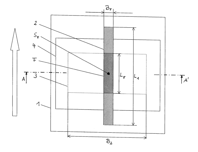
Figure la shows a plan view of the substrate 1 composed
of PET film which has been printed with three
electrical functional layers 2, 3, 4 in order to
produce an electronic component, in this case a diode,
on the surface of the substrate 1. Seen at right angles
to the surface of the substrate 1, the electrical
functional layers 2, 3, 4 are arranged one above the
other and overlapping at least in a surface area F. The
electrical functional layer 2 in this case forms a
first electrical functional layer, with a first length
dimension L1 of the first electrical functional layer
parallel to the surface of the substrate 1 and in the
relative movement direction of the substrate 1 being
formed, during the printing process (shown by an arrow
on the left in Figure la) to be approximately 25 m
longer than a length dimension LF of the surface area F
in the printing direction and parallel to the surface
of the substrate 1. The first electrical functional
layer is composed of electrically conductive material,
in this case copper, as an electrode. The electrical
functional layer 3 forms a second electrical functional
layer, which is separated from the first functional
layer by a third electrical functional layer 4 composed
of poly-3-alkylthiophene. The second electrical
functional layer is formed from silver. The second
electrical functional layer has been formed such that a
second width dimension B2 of the second electrical
functional layer parallel to the surface of the
substrate 1 and at right angles to the relative
movement direction is at least approximately 50 m
wider than a width dimension BF of the surface area F at
right angles to the relative movement direction and
parallel to the surface of the substrate 1. The
electrically conductive supply lines or interconnects
which are, of course, required in order to make
CA 02615285 2008-01-14
- 13 -
electrical contact with the first and second electrical
functional layers have not been illustrated.
Figure la shows the ideal situation in accordance with
the printing layout for the electronic component, in
which the first electrical functional layer is
positioned with respect to the surface area F such that
a first area centroid of the first electrical
functional layer and an area centroid SF of the surface
area F are located one above the other, seen at right
angles to the substrate 1, and the second electrical
functional layer is positioned with respect to the
surface area F such that a second area centroid of the
second electrical functional layer and the area
centroid SF of the surface area F are likewise located
one above the other, seen at right angles to the
substrate 1. In practice, however, this is not the case
because of the discrepancies which occur during the
structuring process.
The layer structure shown in Figure la is tolerant to
any discrepancy or offset such as this of the first
functional layer in the relative movement direction
and/or any discrepancy or offset of the second
functional layer at right angles to the relative
movement direction with respect to the illustrated
ideal case, in accordance with the layout.
Figure lb shows a cross section A-A' through the
printed substrate shown in Figure la, in which the
substrate 1 and the electrical functional layers 2, 3,
4 printed on it can be seen. In this case, the
electrical functional layer 2 forms the first
electrical functional layer, the electrical functional
layer 3 forms the second electrical functional layer,
and the electrical functional layer 4 forms a third
electrical functional layer.
CA 02615285 2008-01-14
- 14 -
Figure 2a shows a plan view of a further printed
substrate 1 composed of PET film, which is printed with
three electrical functional layers 2', 3', 4' in order
to produce an electronic component, in this case a
capacitor, on the surface of the substrate 1. Seen at
right angles to the surface of the substrate 1, the
electrical functional layer 2', 3', 4' are arranged one
above the other and overlapping at least in a surface
area F. The electrical functional layer 2' in this case
forms a first electrical functional layer, with a first
length dimension L1 of the first electrical functional
layer parallel to the surface of the substrate 1 and in
the relative movement direction of the substrate 1
being formed, during the printing of the substrate 1
(shown by an arrow on the left in Figure 2a) to be
approximately 1 mm longer than a length dimension LF of
the surface area F in the relative movement direction
and parallel to the surface of the substrate 1. The
first electrical functional layer is composed of
electrically conductive material, in this case copper,
as an electrode. The electrical functional layer 3'
forms a further electrical functional layer, which is
separated from the first functional layer by a third
electrical functional layer 4' composed of electrically
insulating polymer. The further electrical functional
layer is in the form of a silver electrode.
The first electrical functional layer has been formed
such that a first width dimension B1 of the first
electrical functional layer parallel to the surface of
the substrate 1 and at right angles to the relative
movement direction is approximately 600 m wider than a
width dimension EF of the surface area F at right angles
to the printing direction and parallel to the surface
of the substrate 1. The electrically conductive supply
lines or interconnects which are required to make
electrical contact with the first and further
electrical functional layer have not been illustrated.
CA 02615285 2008-01-14
- 15 -
Figure 2a shows the ideal situation for the printing
layout for the electronic component, in which the first
electrical functional layer is positioned with respect
to the surface area F such that a first area centroid
of the first electrical functional layer and an area
centroid SF of the surface area F are located one above
the other, seen at right angles to the substrate 1, and
the third as well as the further electrical functional
layer are positioned with respect to the surface area F
such that their respective area centroid and the area
centroid SF of the surface area F are likewise located
one above the other, seen at right angles to the
substrate 1. However, in practice this is not the case
because of the discrepancies which occur during the
printing process. The layer structure shown in Figure
2a is tolerant to any discrepancy or offset such as
this of the first functional layer in the relative
movement direction and/or any discrepancy or offset of
the first functional layer at right angles to the
relative movement direction with respect to the
illustrated ideal case in accordance with the printing
layout.
Figure 2b shows a cross section B-B' through the
printed substrate 1 shown in Figure 2a, in which the
substrate 1 and the electrical functional layers 2',
3', 4' printed on it can be seen. In this case, the
electrical functional layer 2' forms the first
electrical functional layer, the electrical functional
layer 3' forms the further electrical functional layer,
and the electrical functional layer 4' forms the third
electrical functional layer.
Figure 3a shows a plan view of a further printed
substrate 1 composed of PET film, which is printed with
two electrical functional layers 2, 3 as an initial
stage in the production of an electronic component, in
this case by way of example an organic field-effect
transistor (OFET), on the surface of the substrate 1.
CA 02615285 2008-01-14
- 16 -
Seen at right angles to the surface of the substrate 1,
the electrical functional layers 2, 3 are arranged one
above the other and overlapping at least in a surface
area F (bounded by a line printed in bold). The
electrical functional layer 2 in this case forms a
first electrical functional layer, with a first length
dimension L1 of the first electrical functional layer
parallel to the surface of the substrate 1 and in a
relative movement direction of the substrate 1 being
formed, during the printing of the substrate 1 (shown
by an arrow on the left in Figure 3a) to be
approximately 1 mm longer than a length dimension LF of
the surface area F in the relative movement direction
and parallel to the surface of the substrate 1. The
first electrical functional layer is formed from semi
conductive material, in this case polyalkylthiophene.
The electrical functional layer 3 forms a further
electrical functional layer. The further electrical
functional layer is formed from silver and is
configured in the form of two comb structures, which
are intended to form the source and drain electrodes of
the OFET. Since the electrical functional layer 3 in
this case has an irregular shape, the surface area F is
in this case defined such that the maximum external
dimensions (in the relative movement direction and at
right angles to it) of the electrical functional layer
3 predetermine the extent of the surface area F, even
though there is no overlap between the two electrical
functional layers at any point within the surface area
F defined in this way. This definition of the surface
area F is expedient in this case since the aim during
the printing of the comb structure with the first
functional layer is to completely cover the comb
structure.
The first electrical functional layer has been formed
such that a first width dimension B1 of the first
electrical functional layer parallel to the surface of
the substrate 1 and at right angles to the relative
CA 02615285 2008-01-14
- 17 -
movement direction is approximately 1 mm wider than a
width dimension BF of the surface area F at right angles
to the relative movement direction and parallel to the
surface of the substrate 1. The electrically conductive
supply lines or interconnects which may be required to
make electrical contact with the first and further
electrical functional layers have not been illustrated.
Figure 3a shows the ideal case in accordance with the
printing layout for the electronic component, in which
the first electrical functional layer is positioned
with respect to the surface area F such that a first
area centroid of the first electrical functional layer
and an area centroid SF.of the surface area F are
located one above the other, seen at right angles to
the substrate 1, and the further electrical functional
layer is positioned with respect to the surface area F
such that its area centroid and the area centroid SF of
the surface area F are likewise located one above the
other, seen at right angles to the substrate 1.
However, in practice, this is not the case because of
the discrepancies which occur during the printing
process. The layer structure shown in Figure 3a is
tolerant to any such discrepancy or offset of the first
functional layer in the relative movement direction
and/or any discrepancy or offset of the first
functional laver at right angles to the relative
movement direction with respect to the illustrated
ideal case in accordance with the printing layout.
Figure 3b shows a cross section C-C' through the
printed substrate 1 shown in Figure 3a, in which the
substrate 1 and the electrical functional layers 2, 3
printed on it can be seen. In this case, the electrical
functional layer 2 forms the first electrical
functional layer, and the electrical functional layer 3
forms a further electrical functional layer.
CA 02615285 2008-01-14
- 18 -
It should be noted that the figure illustrations la to
3b explain the fundamental idea of the invention only
by way of example and that there are many further
options for the person skilled in the art from the
overall context allowing the method according to the
invention to also be used to form electrical functional
layers of other electrical components in continuous
processes, with departing from the subject matter of
the invention in the process.