Note: Descriptions are shown in the official language in which they were submitted.
CA 02615711 2008-01-16
WO 2007/081883 PCT/US2007/000411
THREE-DIMENSIONAL FORCE INPUT CONTROL DEVICE AND
FABRICATION
BACKGROUND
[00011 Field of the Invention
[00021 The present invention relates generally to semiconductor devices, Micro
Electro
Mechanical Systems (MEMS), sensors and more specifically to three dimensional
(3D)
three-axis force sensors integrated with signal processing electronic circuits
on one
substrate. In particular, it relates to three-axis finger force sensors,
finger-mouse and
micro-joysticks for consumer and other applications.
[0003] Background
[0004] 3D force sensors based on micro-machined silicon chips with stress
sensitive
components on flexible diaphragm are known. Prior art shown in Fig.1, uses a
sensor
chip 10 from a rigid frame 12 and rigid central part 16 of a die, boss,
connected with the
frame by a thinner diaphragm 14. An externally applied force is transferred to
the rigid
island 16, the deflection of the island creates deformation and stress in the
elastic
diaphragm element 14, reaching the locations of the stress sensitive IC
components 18,
20, 22. Because the rigid island 16 is located within the thickness dimension
of a die 10
and the width of a circular diaphragm is small and in the sub-millimeter
range, it is very
hard to apply external forces in lateral X and Y directions to the rigid
island 16 to provide
good response, and hence their use is constrained from many consumer devices
and
interfaces.
1
CA 02615711 2008-01-16
WO 2007/081883 PCT/US2007/000411
[0005] In order to resolve this deficiency a rigid force-transferring element
31 is added to
the structure of the die 10 and island 16. This rigid force-transferring
element 31 is
firmly coupled to the rigid island 16 of a sensor die 10 through intermediate
layer 33.
This extension of the rigid island height above the die frame thickness
enhances sensor
sensitivity to the applied vector force in all orthogonal directions. These
components of
force are transferred to a rigid island of the sensor die and then to the
elastic element and
sensitive IC components.
[0006] However, the disadvantages of these kinds of solutions are the
requirement of
additional wafer for the rigid force-transferring elements, additional micro-
machining,
aligning and bonding two wafers, a more complicated process of separating dice
from the
wafer and generally a more expensive fabrication process.
[0007] What is needed are devices that reduce cost of fabrication and
manufacture as
well as providing an easy integration with the higher density IC circuitry on
silicon
substrate.
[0008]
2
CA 02615711 2008-01-16
WO 2007/081883 PCT/US2007/000411
SiTMMARY
The present invention discloses a three-dimensional force input control device
for
sensing vector forces and converting them into electronic signals for
processing in a
electronic signal processing system with all components within a sensor die
fabricated
from the single semiconductor substrate. The typical device comprises a sensor
die
formed within semiconductor substrate, an elastic element within said
semiconductor
substrate, a frame formed around said elastic element and coupled with at
least part of the
periphery of said elastic element all within the substrate, at least three
mechanical stress
sensitive IC components located in the elastic element for providing
electrical output
signals proportional to the mechanical stress in the location of the IC
components, at least
one rigid island element formed in the substrate and coupled with the elastic
element,
this rigid island transfers an external vector force to the elastic element
and through the
IC components which provide electrical output signal, this rigid island has a
height bigger
than the thickness of the frame minus thickness of the elastic element, at
least one spring
element coupling the force-transferring element with an external force and at
least one
electronic circuit for processing output signals from the mechanical stress
sensitive IC
components.
All elements can vary in design and material in order to realize different
aspects
and advantages.
[00091 Several methods of fabrication are disclosed, with a typical method
comprising the
steps of providing a semiconductor substrate having a side one and a side two;
fabricating
stress-sensitive IC components and signal processing IC on side one of the
substrate;
fabricating closed trenches on side two of the substrate, the trenches forming
boundaries
defining elastic elements, frame elements, and rigid islands, trenches for die
separation,
and removing additional substrate material from side two of the substrate in
the frame
area leaving the dimension of the rigid island protruding outward from side
two and
larger than the remaining thickness dimension of the frame minus the thickness
of elastic
element, leaving the rigid island extending outward from the substrate for
coupling with
3
CA 02615711 2008-01-16
WO 2007/081883 PCT/US2007/000411
external force transferring elements or for receiving external mechanical
forces in any
and all directions. Removal of part of the substrate from side two frame
element can be
done by selective etching.
A variation for fabricating closed trenches on side two of the substrate
within a
die area further comprises depositing protective masking layer on side two of
the
substrate; photolithographically defining a pattern of the rigid island,
elastic element,
frame and separating dice trenches, removing masking layer from elastic
element and
separating dice trenches and etching substrate from side two of the substrate
in the elastic
element and separating dice trenches areas to a selected thickness such that
the closed
separating trenches provide the shape and thickness contours in the substrate
for
separating the die in accordance with the defined pattern using less substrate
and
producing less waste.
[00101
4
CA 02615711 2008-01-16
WO 2007/081883 PCT/US2007/000411
BRIEF DESCRIPTION OF DRAWINGS
[0011] Fig.1, shows a prior art 3D force sensor chip with rigid force
transferring island
located within the thickness dimension of a die and additional force
transferring element
connected to the top portion of the rigid island.
[0012] Fig. 2 shows an isometric top and bottom views of a force sensor die
and its major
micro-constructive elements according to an embodiment of the present
invention.
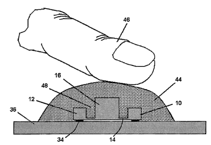
[0013] Fig. 3 shows the principle of a 3-dimensional input finger control of
different
functions in hand-held devices, where 3D force sensor die is connected to the
external
button for applying the force through a spring like element allowing control
to achieve
the required combination of sensitivity, range and accuracy of applied force
or deflection
according to an embodiment of the present invention.
[0014] Fig. 4 shows an example of a flat low profile finger force control
device based on
elastomeric button directly connected to the force sensor die in accordance
with an
embodiment of the present invention.
[0015] Fig. 5 illustrates a flat finger force control device with an
elastomeric button
directly connected to the rigid force-transferring element and comprising a
tactile
sensation mechanical feedback for sensing the click of a depressed button in
accordance
with an embodiment of the present invention.
[0016] Fig. 6 shows an example of a joystick type finger force control device
based on a
elastomeric protrusion body spring back deformable element directly coupled
with the
rigid force-transferring element transferring the force vector to the sensor
die mounted on
the intermediate substrate die in accordance with an embodiment of the present
invention.
[00171 Fig. 7 shows another example of a flattened head joystick type finger
force
control device, where sensor die is mounted directly to the PCB in accordance
with an
embodiment of the present invention.
CA 02615711 2008-01-16
WO 2007/081883 PCT/US2007/000411
10018] Fig. 8 shows an example of a flexing flat head finger force control
device
comprised of a rocking elastic plastic button directly coupled to a rigid
force-transferring
element of a force sensor die and embedded in a layer of plastic, which serves
as an
integrated button die in accordance with an embodiment of the present
invention.
[0019] Fig. 9 shows another example of a flexing flat head finger force
control device
comprised of a rocking elastic plastic button directly coupled to a rigid
force-transferring
element of a force sensor die and comprising a tactile mechanical feedback on
the surface
of the button for a tactile sensation mechanical feedback responsive to button
depression
in accordance with an embodiment of the present invention.
[0020] Fig. 10 shows an example of finger force control device based on
elastomeric
package directly connected to the rigid force-transferring island and
comprising
connections with different buttons depending with various design die in
accordance with
an embodiment of the present invention.
[0021] Fig. 11 shows an example of a flat finger force control device with an
additional
force-transferring element and a springy shell for sensing the click of a
depressed button
in accordance with an embodiment of the present invention.
[0022] Fig. 12 shows another example of a flexing flat head finger force
control device
comprised of a rocking elastic plastic button directly coupled to an
additional force-
transferring element having increased bonding force to the plastic button and
comprising
a tactile mechanical feedback on the surface of the button for a tactile
mechanical
feedback responsive to button depression in accordance with an embodiment of
the
present invention.
[0023] Fig. 13 shows an example of a fabrication process based on the local
etching of
the diaphragm first and then thinning the die frame in accordance with an
embodiment of
the present invention.
[0024] Fig. 14 shows an example of a fabrication process based on the local
etching of
the diaphragm to a certain depth, and then thinning the die frame and
continuing etching
6
CA 02615711 2008-01-16
WO 2007/081883 PCT/US2007/000411
the diaphragm at the same time in accordance with an embodiment of the present
invention.
(0025] Fig. 15 shows an example of a fabrication process based on the local
etching of
the diaphragm first, then depositing a mask layer on the diaphragm area and
then thinning
the frame by etching die in accordance with an embodiment of the present
invention.
[00261 Fig. 16 shows an example of a fabrication process based on deposition
of two
layers of masking materials and two lithographic processes allowing etching a
step
profile fabricating the diaphragm area and thinning the frame in accordance
with an
embodiment of the present invention.
[0027] Fig. 17 shows an example of a fabrication process based on deposition
of one
layer of masking material and two lithographic processes allowing etching a
step profile
fabricating the diaphragm area and thinning the frame die in accordance with
an
embodiment of the present invention.
[0028] Fig. 18 shows an example of a fabrication process based on deposition
of one
layer of masking material and two lithographic processes allowing etching an
elastic
element, separating trenches for dicing and thinning the frame at the same
time in
accordance with an embodiment of the present invention.
[0029] Fig. 19 illustrates additional steps in fabrication of an alternate
larger surface for
force-transferring element, for providing stronger adhesion between the pin
and the
plastic material on the top of the die, in accordance with the another
embodiment of the
invention.
[0030] Fig. 20 illustrates another additional steps in fabrication of an
altemate larger
surface for force-transferring element, for providing stronger adhesion
between the pin
and the plastic material on the top of the die and providing additional force
overload
protection, in accordance with the another embodiment of the invention.
[0031]
7
CA 02615711 2008-01-16
WO 2007/081883 PCT/US2007/000411
DETAILED DESCRIPTION
[0032] Specific embodiments of the invention will now be described in detail
with
reference to the accompanying figures.
[0033] In the following detailed description of embodiments of the invention,
numerous
specific details are set forth in order to provide a more thorough
understanding of the
invention. However, it will be apparent to one of ordinary skill in the art
that the
invention may be practiced without these specific details. In other instances,
well-known
features have not been described in detail to avoid unnecessarily complicating
the
description.
[0034] OBJECTS AND ADVANTAGES
[0035] An object of the present invention is to provide a 3-dimensional force
input
control device for high volume consumer markets like cell phones, portable
gamers,
digital cameras, etc.
[0036] Another object of the present invention is to provide a method of
fabrication of a
3-dimensional force input control device used for integrating in various
functions in
electronic devices.
[0037] Another object of the present invention is to provide a low cost 3-
dimensional
force input control device.
[0038] Another object of the present invention is to provide a finger tip size
3-
dimensional force input control device.
[0039] Another object of the present invention is to provide a high
reliability 3-
dimensional force input control device.
[0040] Another object of the present invention is to provide a high stability
3-
dimensional force input control device.
8
CA 02615711 2008-01-16
WO 2007/081883 PCT/US2007/000411
[0041] Another object of the present invention is to provide a 3-dimensional
force input
control device, which accommodates a sufficiently low noise ratio between
X,Y,Z
sensitivities.
[0042] Another object of the present invention is to provide a 3-dimensional
force input
control device, which has low cross-axis sensitivity.
[0043] Another object of the present invention is to provide a 3-dimensional
force input
control device; which allows process integration with other sensors and CMOS.
[0044] Another object of the present invention is to provide a 3-dimensional
force input
control device, which is scalable.
[0045] Another object of the present invention is to provide a 3-dimensional
force input
control device with required combination of applied force and deflection.
[0046] Another object of the present invention is to provide a 3-dimensional
force input
control device, which enables better economics of manufacturability for high
volume
consumer markets.
[0047] PREFERRED EMBODIMENTS
[0048] Figs. 2-13 show various embodiments of 3D force input control devices,
dice
microstructures and fabrication methods. The detailed description of the
microstructures,
devices and methods of fabrication according to the present invention are
presented
below.
[0049] Referring to embodiments in Figs. 2(a)-(b), the isometric and a cross
section view
of the top planar side of a force sensor die and its major micro-constructive
elements are
shown. The isometric bottom side reflection and cross sectional view of the
die are
shown in Fig.2b. The die 10 has frame 12 surrounding an elastic element 14. In
this
embodiment the elastic element 14 is circular and acts as a diaphragm. A
central rigid
island 16 is coupled to and within the center of the diaphragm 14. On a
circular
diaphragm 14 planar top side there are a number of areas 18, 20, 22 where
mechanical
stress sensitive IC components are effectively located. The IC components 18,
20, 22 are
located on the periphery of the diaphragm adjacent to a frame 12, and
electrically
9
CA 02615711 2008-01-16
WO 2007/081883 PCT/US2007/000411
connected to contact pads 24 26 28 30 32 without metal conductors on the
surface of a
diaphragm. This configuration yields better sensor stability. Stress sensitive
IC
components 18 20 22 can also be located on the other areas of the diaphragm,
for
example in the areas 19,21,23, as shown in Fig. 2a.
[0050] The stress sensitive components occupy a relatively small area on the
surface of
the die. The majority of the area is used for integration of the signal
processing IC. These
IC can be located on the frame area 11, or on the rigid island area 13 or even
on the
elastic element area 14. As the process of stress sensitive components is
compatible with
the regular CMOS process, then any integrated circuit, which can be fabricated
with
CMOS process, can be integrated at the same die. In particular these
integrated IC can
provide the functions of analog signal amplification, analog analog-to-digital
and digital-
to-analog conversion, multiplexing, signal processing, gate logic, memory,
digital
interface, power management, encryption, compression and decompression, mixed
signal
processing, transmitting and receiving wireless signals, sensing various
physical domains
other than force and combinations.
[0051] An externally applied force is transferred to the rigid island 16, the
deflection of
the island creates deformation and stress in the elastic diaphragm element 14,
reaching
the locations of the stress sensitive IC components 18, 20, 22. These at least
three
sensitive IC components create a unique combination of the signals relative to
a specific
value and direction of the applied vector force. Calibration and processing
sensor signals
by integrated IC allows determination of the values of the force vector
components and
therefore also the value and a direction of the externally applied force.
[0052] In another embodiment, illustrated in the Fig.2, the rigid island 16
located within
the die 10 protrudes out from tlie frame 12, or has larger dimension of height
than the
thickness of the frame 12 minus the thickness of the diaphragm 14. It allows
more
efficiently apply an external force in lateral X and Y directions, provides
high sensitivity,
and simplifies the geometrical microstructure of the sensor die. The cost of
manufacturing of the device is consequently reduced substantially due to the
elimination
of need for an additional wa:l-er and corresponding processing steps. The
described
CA 02615711 2008-01-16
WO 2007/081883 PCT/US2007/000411
embodiment microstructure enhances sensor sensitivity to the applied vector
force in all
three orthogonal directions. These components of force are transferred
directly to a rigid
island of the sensor die and then to an elastic element and sensitive IC
components.
[0053] The challenge of practical application of 3D force sensors, as input
force
controlled devices, is that the deflection of the rigid island 16 in semi-
conductor type
materials is negligible. The psychological response to the control of the
applied force is
based on the applied force or, for example pressure on the finger. For good
finger
control, some range of deflection is required, and this range would also
increase the
accuracy of applying input signals matching a range of applied force and
sensitivity of
the device.
,[0054] An aspect of the invention resolving this issue is illustrated in
Fig.3 according to a
third embodiment. A two ended spring element 40 is added to a sensor. The
first end of
spring element 40 is coupled to a rigid island 16 of a sensor die 10, which
has a frame 12
and contact pads 34. The second end of the spring element 40 is connected to a
button 42,
where the external force vector is applied. The spring element 40 phases the
deflection,
increases the range of motion or applied force and accuracy of the input
mechanical
signal. As another benefit, the spring element 40 also increases the range of
the
opportunities in designing the microstructure of the sensor die for better
performance
from variable stiffness, reliability and cost.
[00551 As illustrated in Fig.4, for some finger mouse applications, there is a
need for a
small but responsive deflection of a button and input force controlled
devices. These are
satisfied by shaping a flat button according to another embodiment of the
invention. A
sensor die 10 is bonded to a substrate 36 with the contact pads 34. The sensor
die 10 is
covered with elastic plastic materia144 forming a desired shape of a button.
[0056] The external force is applied to an elastic button, for example by a
finger 46.
Norrnal and sheer force are transferred through the elastic material of a
button to the rigid
island 16, elastic element 14 and finally to the stress sensitive IC
components, result in
output electrical signals proportional to an applied external force.
11
CA 02615711 2008-01-16
WO 2007/081883 PCT/US2007/000411
[00571 The size of a sensor die and the viscosity and elasticity of an elastic
material of
the plastic button determine the response characteristics of the sensor to a
large degree.
The elastic plastic material 44 covers the sensor die 10 directly from the
back profiled
side and might filling in the cavity 48 between the frame 12 and the rigid
island 16.
Normal and sheer force applied by a force are transferred through the elastic
material of a
button directly to the rigid island 16 and then to the stress sensitive IC
components.
In many applications X and Y components of a force vector are used for a
navigation by cursor on the screen of an electronic device while. When
position of a
cursor is selected then the action button is actuated. In most cases this
action button is
separated from the X-Y cursor navigation system like in finger point mouse of
IBM
Think Pad. Action button especially in portable devices preferably requires
mechanical
feedback or mechanical clicking function, which can be sensed by tactile
sensors of the
finger. As proposed finger force control device combines X,Y'and Z control
functions in
one 3D sensor, Z control can be used as an action button eliminating the need
for a
separate control action button. The mechanical clicking feedback function can
be
incorporated in the device, as illustrated in Fig.5, according to the fifth
embodiment of
the present invention.
[0058] The sensor die 10 is bonded to a substrate 36 with the contact pads 34.
The
sensor die 10 is covered with elastic plastic material 44 forming a desired
shape of a
button. The external force is applied to an elastic button, for example by a
finger 46.
Normal and Sheer force are transferred through the elastic material of a
button to the
rigid island 16, elastic element 14 and finally to the stress sensitive IC
components,
which result in output electrical signals proportional to X and Y components
of the
external force.
[0059] In the top portion of the elastic plastic button the tactile sensation
mechanical
feedback allows sensing the click of the pressed button, because it has a
springy shell
structure 50 with the cavity 52 beneath. When pressed from the top it buckles
slightly,
retaining continuity but sending a click sensation to the finger 46. This
springy shell can
be made from different materials including metals and plastics. The buckling
action
creates not only a tactile feedback but also generates short pulses in the
mechanical
12
CA 02615711 2008-01-16
WO 2007/081883 PCT/US2007/000411
sensitive components, which can be used as signals for activation of certain
electronic
action.
[0060] As illustrated in Fig.6, the spring element 54 providing required range
of
deflection and sensitivity can be made from the elastic plastic material
according to sixth
embodiment. In this embodiment the sensor die 10 and the rigid force-
transferring island _
16 are mounted on the intermediate substrate 53, which has contact pads 54.
The elastic
plastic package material 55 covers the above elements and forms a flexible
protrusion.
The extended end of the protrusion 56 serves as a button for tactile contact.
An external
force applied, via finger 46, to a button 56 bends the protrusion 55 creating
mechanical
stress and deflection within the plastic in the device base area 58 between
the sensor die
and the rigid force-transferring island 16. This induced stress is transferred
to the sensor
die and finally to the stress sensitive IC components. This design of a micro-
joystick
allows achieving very low cost in production due to its design simplicity and
existing
well-developed mass manufacturing technologies.
[0061] Another embodiment of a plastic elastic finger joystick with flattened
head 60 at
the protruding end of the stick is shown in Fig.7. The plastic stick 62 can be
fabricated in
various shapes, colors and elasticity, depending on the application and
requirements. In
this embodiment the sensor die 10 is mounted directly to the PCB 36 of an
electronic
device.
[0062] For computer mouse applications at times there is need for small
deflections of a
button as compared with large joystick applications, but the height of an
input control
device can be governing. For these applications, as illustrated in Fig.8, the
spring
element providing required range of deflection and sensitivity can be made as
a low
profile rocking two vertebrae spine design according to another embodiment.
Here, the
sensor die 10 with the rigid force-transferring island 16 is mounted on the
substrate 36.
The elastic plastic 64 covers all above elements and forms a flexible neck 66.
The top
surface of the button is covered with a hard layer of plastic 68 serving as a
surface where
an external force is applied. The force applied, for example by a finger 46,
to the top
hard layer 68 of the button, rocks the button 64 cireating the mechanical
stress and
13
CA 02615711 2008-01-16
WO 2007/081883 PCT/US2007/000411
deflection within the plastic in the neck area 66 between the sensor die 10
and the rigid
force-transferring island 16. This stress is transferred to the sensor die and
finally to the
stress sensitive IC components.
[0063] A flexing flat head finger force control device is shown in Fig.9. It
comprises a
rocking elastic plastic button 64 directly coupled to a rigid force-
transferring island 16 of
a force sensor die and comprising a tactile sensation mechanical feedback 70
on the
surface of the button 68 allowing sensing the click of the pressed button
according to the
another embodiment of the present invention.
[0064] In the top portion of the plastic button 68 the tactile sensation
mechanical
feedback 70 allowing sensing the click of the pressed button is incorporated.
It has a
springy shell structure 70 with the cavity 72 beneath it. When being pressed
from the top
it reaches the threshold after which it buckles, creating a clicking sensation
in the force
applying finger 46. This springy shell can be made from different materials
including
metals and plastics. The clicking action creates not only a tactile feedback
but also
generates a short pulses in the mechanical sensitive components, which can be
used as
signal for activation of other programmable action.
[0065] Many applications and designs of portable devices require various
control buttons
in size, shape, color and material while functionality is maintained. In an
embodiment of
the invention, a detachable button, as illustrated in Fig. 10, can be used..
[0066] The finger force control device has an elastomeric package 80 directly
connected
to the sensor die 10 comprising rigid force-transferring island 16. It also
comprises
means 84, 86 for connecting with different buttons 88. These buttons also have
corresponding and matching means 90, 92 for connecting with control device
package 80.
The external design of the button 88 depends on specific application
requirements. The
button 88 can be either a separate component or can be integrated in the mat
94 of the
keyboard of portable device.
[0067] In some applications, the small surface size of the rigid island pin
might not
provide a long-term strong adhesion between the pin and the plastic material
of the button
attached. An increased surface of the rigid pin can be achieved by fabricating
an
14
CA 02615711 2008-01-16
WO 2007/081883 PCT/US2007/000411
additional force-transferring element 35, as it shown in Fig. 11 according to
the another
embodiment of the present invention. This force-transferring element may have
a hole
where rigid pin can be inserted and mechanically connected to the pin with
either glue, or
solder, or some other attaching mechanism. This force-transferring element can
be made
from different materials, for example from plastic, metal, semiconductor,
ceramic, etc. It
also can be connected and bonded to the pin in a batch fabrication manner, for
example to
the whole wafer or to a number of wafers at the same time.
[0068) An additional force-transferring element 35 can serve, as a platform
for mounting
a springy shell 39, as shown in Fig. 11. This springy shell 39 can be mounted
on the
surface of force-transferring element either individually with automated pick
and place
equipment or in a batch fabrication manner.
[0069] There are different designs. One is that a substrate, with the
additional force-
transferring elements, is bonded to the wafer of force sensor dice and then
with the
substrate of the springy shells. Another design is substrate with the
additional force-
transferring elements bonded first to the substrate of the springy shells and
then to the
wafer with the force sensor dice. The sensor die, the additional force-
transferring
element and the springy shell, after singulation from the wafer, are covered
with plastic
material 44, as shown in Fig. 11, forming an external force-transferring
element for
contact with an external force, eg. a finger 46.
[0070] An additional force-transferring element 35, shown in Fig. 12, can be
more
complex in shape according to another embodiment of the present invention.
This force-
transferring element also can be made from a variety of materials, including
plastic,
metal, semiconductor, ceramic, etc. It also can be connected and bonded to the
pin in a
batch fabrication manner at the wafer level.
[00711 In another embodiment, an additional force-transferring element 35 has
a cavity
41 for accepting the rigid pin 16, which are bonded with adhesive material 43.
There is a
portion 45 which is inserted into the trench 47 proximate to the rigid pin 16
and serves
several purposes. First, it increases the surface of connection with the pin
and
strengthens bonding and reliability of the device. Second, it prevents plastic
64 from
CA 02615711 2008-01-16
WO 2007/081883 PCT/US2007/000411
going into the trench 47 during molding of the external force-transferring
element. Third,
it serves, as an additional stop, limiting mechanical overload in X, Y and Z
directions.
[0072] The additional force-transferring element 35 has cavities or bumps 49,
51 on the
surface of this element for stronger bonding with plastic material 64 of the
external force-
transferring element. It provides higher reliability.
[0073] Fabrication of a 3D force sensor die from a single substrate and for
the lowest
cost represents the biggest challenge. There are several options in batch
fabricating senor
dice.
[0074] Fig. 13a-13d illustrate the fabrication according to the another
embodiment of the
present invention. Fig. 13a shows an initial silicon substrate 100 having
surface one 101
and surface two 102. The wafer initially goes through the standard CMOS
process
fabricating IC circuitry 104, sensitive components 106 and contact pads 108,
as it shown
in Fig. 13b. After a standard CMOS process, a masking layer 103 is deposited
on the
side two of the wafer. A double-side lithography is made from the side two of
the wafer
opening the elastic element area 110, leaving the masking layer 111 on the
frame and the
rigid island, as shown in Fig. 13c. Next a deep local etching of silicon wafer
is applied
from the backside of the wafer forming the trench 112 to the depth for design
dimensions
the elastic element 113. Local etching can be done by different types of dry
or wet
etching known in the art, for example by RIE, dry plasma etching, electro-
sparking, wet
isotropic and anisotropic etching, etc. After that silicon is removed locally
from the frame
elements 114 backside of the wafer, as it shown in Fig. 13d. As a result, the
height
dimension of the rigid islands 116 becomes larger than the remaining thickness
if the
frame 114 minus thickness of the elastic element 113. The last step of
removing silicon
from the frame area can be done by different ways including mechanical
milling, electro-
sparking, abrasive milling and different kind of etching, dry and wet.
[0075] Fig. 14a-14d illustrates a fabrication method according to another.
,embodiment of
the present invention. Fig. 14 a shows an initial silicon substrate 100 having
front surface
(side one) 101 and back surface (side two) 102. The wafer first goes through
the standard
CMOS process fabricating IC circuitry 104, sensitive components 106 and
contact pads
16
CA 02615711 2008-01-16
WO 2007/081883 PCT/US2007/000411
108, as it shown in Fig. 14a. After a standard CMOS process, a masking layer
111 is
deposited on the backside of the wafer. A double-side lithography is made from
the
backside of the wafer opening the elastic element 110 and leaving the masking
layer 111
on the frame and 115 on the rigid island, as shown in Fig. 14b. Next a deep
local etching.
of silicon wafer is made from the backside of the wafer forming the trench 112
to the
depth equal to the difference between the final thickness of the frame and
design
thickness of the elastic element 113. This local etching can be done by
different types of
dry or wet etching known in the art, RIE, dry plasma etching, electro-
sparking, wet
isotropic, anisotropic etching, etc. Next that masking layer 111 is removed
from the
frame element 118, as shown in the Fig. 14c. The etching process from the
backside of
the wafer continues etching elastic element and frame element simultaneously,
shown in
Fig. 14d. As a result, the height dimension of the rigid island 116 becomes
larger than
the remaining thickness of the frame 114 minus thickness of the elastic
element 113 and
the thickness of the elastic element reaches design thickness. The step of
removing
silicon from the elastic element and frame element can be done in various ways
including
different kind of etching, dry and wet, for example by RIE.
[0076] Fig. 15a-15d illustrate the fabrication method according to yet another
embodiment of the present invention. Fig. 15a shows a silicon substrate 100
having front
surface 101 and back surface 102 after a CMOS process was completed and the
trenches
112 around rigid island 116 were etched forming an elastic element 113. After
that a
masking layer 120 is deposited on the backside of the wafer masking the
sidewalls of the
trenches and the surface of the elastic element 113, as it shown in Fig. 15b.
The next step
is removing a masking layer from the frame area 118, as shown in Fig. 15c
leaving the
mask 115 and 120 on the rigid island and trench including back surface of the
elastic
element 113. Next the silicon is removed locally from the frame areas from the
backside
of the wafer, as it shown in Fig. 15d. As a result, the height dimension of
the rigid
islands 116 becomes larger than the remaining thickness if the frame 114 minus
thickness
of the elastic element 113. The last step of removing silicon from the frame
area can be
done in a variety of ways including different kind of etching, dry and wet.
17
CA 02615711 2008-01-16
WO 2007/081883 PCT/US2007/000411
[0077] One of the challenges in methods described above is removing mask from
the
frame element, when some kind of profile is already fabricated on the backside
of the
wafer. This can be achieved by masking the backside of the wafer by two layers
of
masking materials having etching selectivity to each other and two
lithographic processes
made on the initial flat surface of the wafer backside according to another
embodiment of
the present invention.
[0078] Fig. 16 a shows a silicon substrate 100 having front surface 101 and
back surface
102 after CMOS process. Next two masking layers 122 and 124 are deposited on
the
backside of the wafer, as it shown in Fig. 16a. The masking layer 124 adds
high
selectivity of etching to masking layer 122. The next step is removing the
masking layer
124 from the frame element and elastic element leaving it only on the rigid
islands, as
shown in Fig. 16b. A second lithography follows, opening the elastic element
110 in the
masking layer 122, as shown in the Fig. 16c. As a result, the backside of the
wafer has
three different etched elements: unmasked area 110, frame element masked with
one
masking layer 122 and rigid island element masked with masking layers 122 and
124.
Next the silicon is etched locally in the elastic element through the masks
122 and 124 to
a predetermined depth. Following that the masking layer 122 is etched from the
frame
element 1281eaving the mask 124 on the rigid island, as shown in Fig. 16d. The
next step
is a simultaneous etching of the frame and the elastic elements, as shown in
Fig. 16e. As
a result, the height dimension of the rigid islands 134 becomes larger than
the remaining
thickness of the frame 132 minus thickness of the elastic element 130 and
protrude
outward from the substrate.
[0079] Another. process of a double masking process from the backside of the
wafer is
presented in Fig. 17a-17e according to another embodiment of the present
invention. Fig.
17a shows a silicon substrate 100 having front surface-101 and back surface
102 after
CMOS process. Next a masking layers 136 is deposited on the backside of the
wafer
102, shown in Fig. 17a. The next step is removing a masking layer 136 from the
frame
and from the elastic element leaving the layer only on the rigid islands,
shown in Fig.
17b. A second lithography follows, opening the elastic element 110, as shown
in the Fig.
17c. As a result, the backside of the wafer has three different areas:
unmasked area 110,
18
CA 02615711 2008-01-16
WO 2007/081883 PCT/US2007/000411
frame element masked with photoresist layer 138 and rigid island element
masked with
masking layer 136. On the next step silicon is etched locally in the elastic
element area
through the masks 136 and 138 to a predetermined depth. Next the masking
photoresist
layer 138 is etched off the frame 128 leaving the mask 136 on the rigid
island, as shown
in Fig. 17d. The final step is a simultaneous etching of the frame and the
elastic element,
shown in Fig. 17e. As a result, the height dimension of the rigid islands 134
becomes
larger than the remaining thickness of the frame 132 minus thickness of the
elastic
element 130.
[00801 The deep etching of the trenches surrounding the rigid islands also
etches a
substantial part of the wafer thickness, and this process can also be useful
for the purpose
of singulating the dice from the wafer without conventional dicing, reducing
the overall
cost of the 'device in accordance with another embodiment of the present
invention.
[0081] Fig. 18a shows a silicon substrate 100 after CMOS process with the
substrate
backside of the wafer masked in the rigid islands with the masking layer 136.
The
second lithography is following up opening the elastic element 110 and dicing
trenches
140, as shown in the Fig. 18b. As a result, the backside of the wafer has four
different
areas: unmasked elastic element area 110, unmasked dicing trenches 140, frame
masked
with photoresist layer 138 and rigid island masked with masking layer 136. On
the next
step silicon is etched locally in the elastic element 126 and in the dicing
trenches 142
through the masks 136 and 138 to a predetermined depth. Next the masking
photoresist
layer 138 is etched from the frame area 144 leaving the mask 136 on the rigid
island, as
shown in Fig. 18c. A simultaneous etching of the frame, the elastic elements
and dicing
trenches occurs, shown in Fig. 18d. As a result, the height dimension of the
rigid islands
134 becomes protruded from the substrate, over the remaining thickness of the
frame
132. This occurs simultaneously with the formation of the dicing trenches 146
for
singulatiion of the dice from the wafer.
[0082) Fig. 19 illustrates additional steps in fabrication process, according
to the another
embodiment. These steps allow fabricating an additional force-transferring
element 150,
as it shown in the Fig. 19. This force-transferring element has much larger
surface as
19
CA 02615711 2008-01-16
WO 2007/081883 PCT/US2007/000411
compared to the surface of the rigid pin 134. It provides a long-term strong
adhesion
between the pin and the plastic material on the top of the die.
[0083] Fig. 19 a shows the completed sensor wafer with the rigid pins
protruding from
the surface of the substrate wafer. The mechanical substrate wafer 149 is then
aligned
with the sensor wafer 129 so that pins 134 go through the coupling holes 153
in the
substrate 149. Then two wafers are bonded together with material 154, 156.
This material
can be adhesives, solder, or other material creating strong and rigid bonding
between two
wafers. The individual elements 150 might be separated from each other at the
wafer
level by the combination of slots and bridges 152, as it shown in Fig.19b.
These slots and
bridges are fabricated in the substrate, as holes for the pins are fabricated
for mating. At
this point the bonded wafers can be diced and application of plastic material
on the top of
the die for forming external force-transferring element can proceed.
[0084) As a continuation of this embodiment, Fig. 19c illustrates additional
steps in
fabrication process. These steps include mounting springy shells 158, as shown
in Fig.
19c. These springy shells 158 can be mounted on the surface of force-
transferring
elements 150 either individually with automated pick and place equipment or in
a batch
fabrication manner. Next the bonded wafers with springy shells can be diced
and/or
application of plastic material on the top of the die for forming external
force-transferring
elements in a batch process.
[0085] Fig. 20 illustrates the back-end of fabrication process according to
another
embodiment of the invention. Fig. 20a shows the completed sensor wafer with
the rigid
pins protruding from the surface of the wafer. The mechanical substrate or
wafer 161 is
provided. This mechanical substrate can be made from different materials, for
example
from plastic, metal, semiconductor, ceramic, etc. At least one surface of this
mechanical
substrate has been profiled in such a way that the cavities 166 for accepting
the rigid pins
134 are formed. The other micro-structural elements such as ridges 168,
cavities 172 and
cavities or trenches 170 along with the other designed micro-structural
elements could be
fabricated at the same time with the cavities 166 for the pins 134. The
mechanical
substrate is aligned with the sensor wafer 129 so that pins 134 go into the
cavities 166 in
CA 02615711 2008-01-16
WO 2007/081883 PCT/US2007/000411
the mechanical substrate 161. The depth of the cavity 166, the height of the
pin 134 and
the thickness of the bonding material 164 all together determine the gap 165
between the
frame of the sensor wafer 129 and the additional force-transferring element
162. At the
same time ridges 168 go into the closed trench 131 around the pin 164. At the
next step
two wafers are bonded together with bonding material 164. This material can be
either
different kind of adhesives or solder, or other material creating strong and
rigid bonding
between two wafers. The individual elements 162 might be separated from each
other at
the substrate level by the combination of slots and bridges 174, as it shown
in Fig.20b.
These slots and bridges are fabricated in the mechanical substrate at the same
time, as the
other micro-structural elements 166, 168, 170, 172 are fabricated. At this
stage the
bonded wafers are -diced and then plastic material 176 is applied on the top
of the dice in
a batch-manufacturing manner for forming external force-transferring elements,
as it
shown in Fig.20c. In the process of molding the material 176 the external
force-
transferring elements this material will go into the cavities 170, 172
creating strong and
reliable mechanical connection with the additional force-transferring element
162. At the
same time the small gaps 165 and the ridges 168 would prevent plastic material
176 from
going into the closed trenches 131 around the pin 134.
[00861 Is should be noted, that the fabrication of the devices, according to
this invention,
on a common substrate carries inherent advantages from integration with other
analog
and digital circuits, circuits which provide but are not limited to analog
signal
amplification, analog-to-digital and digital-to-analog conversion,
multiplexing, signal
processing, gate logic, memory, digital interface, power management,
encryption,
compression and decompression, mixed signal processing, transmitting and
receiving
wireless signals, sensing components of other than force physical domains and
combinations.
[0087] It should be understood that the microstructures of the die, structures
of the
finger-mice, finger buttons and micro-joysticks and methods of their
fabrication do not
limit the present invention, but only illustrate some of the various technical
solutions
covered by this invention. While the invention has been described in detail
with
21
CA 02615711 2008-01-16
WO 2007/081883 PCT/US2007/000411
reference to preferred embodiments, it is understood that variations and
modifications
thereof may be made without departing from the true spirit and scope of the
invention.
[0088] Therefore, while the invention has been described with respect to a
limited
number of embodiments, those skilled in the art, having benefit of this
invention, will
appreciate that other embodiments can be devised which do not depart from the
scope of
the invention as disclosed herein. Other aspects of the invention will be
apparent from
the following description and the appended claims.
22