Note: Descriptions are shown in the official language in which they were submitted.
CA 02617314 2007-10-05
WO 2006/105644 PCT/CA2006/000500
MOUNTING ASSEMBLY
FOR OPTOELECTRONIC DEVICES
FIELD OF THE INVENTION
[0001] The present invention pertains to the field of illumination systems and
in
particular to a mounting technology for optoelectronic devices.
BACKGROUND
[0002] Advances in the development and improvements of the luminous flux of
light-
emitting devices such as solid-state semiconductor and organic light-emitting
diodes
(LEDs) have made these devices suitable for use in general illumination
applications,
including architectural, entertainment, and roadway lighting. Light-emitting
diodes are
becoming increasingly competitive with light sources such as incandescent,
fluorescent,
and high-intensity discharge lamps.
[0003] Light-emitting diodes offer a number of advantages and are generally
chosen
for their ruggedness, long lifetime, high efficiency, low voltage
requirements, and the
possibility to control the colour and intensity of the emitted light
independently. Light-
emitting diodes provide an improvement over delicate gas discharge lamp,
incandescent
or fluorescent lighting systems. Solid- state semiconductor and improvingly
organic
light-emitting diodes have the capability to create the same outstanding
lighting
impressions.
[0004] Unlike classical incandescent light sources which can emit almost all
of the
generated waste heat in the form of infrared radiation, most of the heat
generated in
LEDs is first absorbed by the material structures comprising the optically and
electrically active regions inside the LED die. The LED die itself therefore
can obstruct
heat transfer to the environment. Despite the higher electro-optical
conversion
efficiency, thermal management is of particular relevance in LED luminaire
design. The
efficiency and longevity of light-emitting diodes is strongly affected by
temperature and
hence LEDs typically require combinations of passive or active cooling
mechanisms in
order to maintain acceptable operating temperature conditions. For fixed
parameters
such as packaging and employed LED die materials, factors of aging such as the
CA 02617314 2007-10-05
WO 2006/105644 PCT/CA2006/000500
durability and reliability of light-emitting diodes are substantially governed
by operating
temperature conditions.
[0005] In this respect, the mounting technology of LED die and LED packages is
of
particular importance in managing the device operating temperature
effectively.
[0006] LED die or packages together with other components can be placed on a
thermally well conducting single carrier for example a metal core printed
circuit board
(MCPCB) or a ceramic carrier (for example a low temperature co-fired ceramic
on metal
substrate). The MCPCB absorbs and disperses heat from the LEDs; however, it
heats
up. Consequently, using a thermally well conducting carrier for high density
LED
mounts, typically raises the operating temperature for all other components
attached to
the MCPCB. Furthermore the placement of LED die or packages on top of the
carrier
adds further layers that the heat has to propagate through in order to be
conducted away
from the LEDs, thereby resulting in increased thermal resistance.
[0007] United States Patent Application No. 2005/0243558 describes a lamp
assembly
and methods of assembling same. The lamp assembly comprises a printed circuit
board
(PCB) having a face surface, a rear surface opposite the face surface,
electrical traces on
the rear surface, and an opening extending from the face surface to the rear
surface, and
a LED emitter having a dome portion, a body, and a plurality of electrical
terminals
connected to the body, wherein the body of the LED emitter is adjacent the
rear surface,
the dome portion of the LED emitter extends through the opening in the PCB to
the face
surface, and the electrical terminals are connected to the electrical traces
on the rear
surface. This configuration of the lamp assembly, however, requires a very
thin PCB
such as a flexible circuit board in order to be optically efficient. This
patent application
focuses on the visibility of the electrical traces for direct viewing and does
not try to
improve thermal access and reduce thermal resistance to the LED packages
utilized.
[0008] United States Patent No. 6,930,332 describes a light-emitting device
that can
provide enhanced heat radiation as well as allowing light from a LED chip to
be
efficiently extracted out of the device. This light-emitting device includes a
metal plate
that is made of aluminum. The metal plate has a projection projecting forward
and the
projection has a front side provided with a housing recess. A LED chip is
mounted on
the bottom of the housing recess so that it is thermally coupled to the metal
plate, thus
2
CA 02617314 2007-10-05
WO 2006/105644 PCT/CA2006/000500
allowing heat to be radiated. A PCB, having a glass epoxy substrate is joined
to the
front surface of the metal plate and is provided with an insertion hole into
which the
projection is inserted. The LED chip and a bonding wire are encapsulated in a
transparent resin seal portion. The side wall of the housing recess that is
part of the
metal plate functions as a reflector for reflecting forward the light emitted
from the LED
chip. Thus, light from the LED chip can be extracted efficiently. In this
configuration,
the substrate and heat sink are formed as one unit and configured
substantially as a heat
spreader similar to a MCPCB. Additionally the PCB and the components mounted
thereto will essentially reach the same temperature as the metal substrate as
the parts are
in intimate thermal contact.
[0009] Therefore there is a need for a mounting assembly that can enhance the
thermal
management of the optoelectronic devices.
[0010] This background information is provided to reveal information believed
by the
applicant to be of possible relevance to the present invention. No admission
is
necessarily intended, nor should be construed, that any of the preceding
information
constitutes prior art against the present invention.
SUMMARY OF THE INVENTION
[0011] An object of the present invention is to provide a mounting assembly
for
optoelectronic devices. In accordance with an aspect of the present invention,
there is
provided a light-emitting apparatus connectible to a thermal management
system, the
apparatus comprising: a carrier including one or more light transmission
regions; and
one or more light-emitting elements for generating light, each of the one or
more light-
emitting elements mounted on a substrate having a cooling interface, the
substrate being
inferiorly mounted onto the carrier in order that each of the one or more
light-emitting
elements are proximate to one of the one or more light transmission regions,
wherein the
cooling interface is directed away from the carrier and is adapted for
connection to a
thermal management system; wherein the one or more light-emitting elements are
adapted for connection to a source of power for activation thereof.
[0012] In accordance with another aspect of the invention, there is provided a
light-
emitting apparatus connectible to a thermal management system, the apparatus
3
CA 02617314 2007-10-05
WO 2006/105644 PCT/CA2006/000500
comprising: a carrier including one or more light transmission regions; and
one or more
light-emitting elements for generating light, each of the one or more light-
emitting
elements having a cooling interface, said light-emitting elements being
directly
inferiorly mounted onto the carrier in order that each of the one or more
light-emitting
elements are proximate to one of the one or more light transmission regions,
wherein
each cooling interface is directed away from the carrier and each cooling
interface is
adapted for connection to a thermal management system; wherein the one or more
light-
emitting elements are adapted for connection to a source of power for
activation thereof.
[0013] In accordance with another aspect of the present invention, there is
provided a
method for forming a light-emitting apparatus connectible to a thermal
management
system, the method comprising the steps of: providing a carrier having one or
more light
transmission regions; aligning one or more light-emitting elements with one of
the light
transmission regions, each of the one or more light-emitting elements having a
cooling
interface; inferiorly coupling the one or more light-emitting elements to the
carrier;
thereby forming the light-emitting apparatus.
BRIEF DESCRIPTION OF THE FIGURES
[0014] Figure 1 illustrates a mounting assembly according to one embodiment of
the
present invention.
[0015] Figure 2 illustrates a mounting assembly according to another
embodiment of
the present invention.
[0016] Figure 3A illustrates a mounting assembly according to another
embodiment of
the present invention.
[0017] Figure 3B illustrates the housing or package of the light-emitting
element of
Figure 3A.
[0018] Figure 4 illustrates a mounting assembly which is in thermal contact
with a
thermal management system according to one embodiment of the present
invention.
[0019] Figure 5 illustrates multiple mounting assemblies which are in thermal
contact
with a thermal management system according to one embodiment of the present
invention.
4
CA 02617314 2007-10-05
WO 2006/105644 PCT/CA2006/000500
[0020] Figure 6 illustrates a mounting assembly in which a substrate forms an
integral
body with part of a thermal management system according to one embodiment of
the
present invention.
[0021] Figure 7 illustrates a mounting assembly with an integrated variable
focal-
length fluid lens according to one embodiment of the present invention.
[0022] Figure 8A illustrates a mounting assembly with a light-emitting element
which
is directly affixed to a carrier according to one embodiment of the present
invention.
[0023] Figure 8B illustrates a light-emitting element which can be directly
affixed to a
carrier according to one embodiment of the present invention.
[0024] Figure 8C illustrates a light-emitting element which has a textured
emission
window according to one embodiment of the present invention.
[0025] Figure 8D illustrates a light-emitting element is affixed to a carrier
according
to one embodiment of the present invention.
[0026] Figure 8E illustrates a light-emitting element which is affixed to a
carrier with
multiple conducting planes according to one embodiment of the present
invention.
[0027] Figure 9 illustrates a mounting assembly of attached light-emitting
elements
which is in thermal contact with a two stage thermal management system
according to
one embodiment of the present invention.
[0028] Figure 10 illustrates a mounting assembly with a transparent carrier
according
to one embodiment of the present invention.
[0029] Figure 11 illustrates a mounting assembly according to another
embodiment of
the present invention.
[0030] Figure 12 illustrates the mounting assembly as illustrated in Figure
11, with a
connecting secondary optic and a thermal management system.
CA 02617314 2007-10-05
WO 2006/105644 PCT/CA2006/000500
DETAILED DESCRIPTION OF THE INVENTION
Definitions
[0031] The term "light-emitting element" is used to define any device that
emits
radiation in any region or combination of regions of the electromagnetic
spectrum for
example, the visible region, infrared and/or ultraviolet region, when
activated by
applying a potential difference across it or passing a current through it, for
example.
Therefore a light-emitting element can have monochromatic, quasi-
monochromatic,
polychromatic or broadband spectral emission characteristics. Examples of
light-
emitting elements include semiconductor, organic, or polymer/polymeric light-
emitting
diodes, optically pumped phosphor coated light-emitting diodes, optically
pumped nano-
crystal light-emitting diodes or any other similar light-emitting devices as
would be
readily understood by a worker skilled in the art. Furthermore, the term light-
emitting
element is used to define the specific device that emits the radiation, for
example a LED
die, and can equally be used to define a combination of the specific device
that emits the
radiation together with a housing or package within which the specific device
or devices
are placed.
[0032] The term "thermal management system" is used to define an element
providing
a means for thermal energy transfer. A thermal management system can be
designed to
incorporate thermal removal techniques including but not limited to conductive
and
convective cooling, liquid cooling, phase change cooling and forced air
cooling.
Thermal management systems can comprise heat pipes, thermosyphons,
thermoelectrics,
thermotunnels, heat spreaders, heat sinks, spray cooling systems, macro or
micro
channel cooling systems, thermoelectric cooling systems or other appropriate
thermal
management systems as would be known to a worker skilled in the art.
[0001] As used herein, the term "about" refers to a+/-10% variation from the
nominal
value. It is to be understood that such a variation is always included in any
given value
provided herein, whether or not it is specifically referred to.
[0033] Unless defined otherwise, all technical and scientific terms used
herein have
the same meaning as commonly understood by one of ordinary skill in the art to
which
this invention belongs.
6
CA 02617314 2007-10-05
WO 2006/105644 PCT/CA2006/000500
[0034] Thermal management is a key to ensure appropriate thermal operating
conditions of light-emitting elements, wherein these light-emitting elements
can
generate high amounts of waste heat in concentrated small spaces and typically
require
effective cooling. In addition a level of thermal isolation between the light-
emitting
elements and other necessary temperature sensitive components can be required
in order
to limit the thermal impact that the light-emitting elements have on these
temperature
sensitive components.
[0035] The present invention provides a mounting assembly for one or more
light-
emitting elements, wherein the mounting assembly is configured such that the
one or
more light-emitting elements are inferiorly connected to a carrier. The
carrier comprises
one or more light transmission regions, wherein each of the one or more light-
emitting
elements is aligned with a light transmission region enabling light to pass
through the
carrier. The inferior mounting of the light-emitting elements can provide ease
of
thermal access to a cooling interface associated with each of the one or more
light-
emitting elements by a thermal management system.
[0036] In one embodiment of the present invention the light-emitting elements
are
mounted on a thermally conductive substrate and this assembly is in turn
inferiorly
mounted to the carrier. In another embodiment of the present invention, the
light-
emitting elements are directly inferiorly mounted to the carrier wherein a
surface of the
light-emitting element interfaces directly with the carrier.
[0037] Due to the inferior mounting of the one or more light-emitting elements
relative to the carrier, the emission of light generated by the one or more
light-emitting
elements will be directed at the carrier and therefore the one or more light
transmission
regions provide a means for light transmission through the carrier. In one
embodiment
of the present invention the one or more light transmission regions are
defined by
openings or apertures formed within the carrier. Alternately, a transparent
carrier or
regions of transparency defined in the carrier can provide the one or more of
the light
transmission regions.
[0038] In one embodiment, the number and thickness of layers between the one
or
nlore light-emitting elements and the thermal management system are reduced in
7
CA 02617314 2007-10-05
WO 2006/105644 PCT/CA2006/000500
comparison to current solutions thereby resulting in improved thermal
performance and
reduced junction temperature.
[0039] The inferior mounting of the one or more light-emitting elements
relative to the
carrier can provide a level of thermal isolation of the carrier from the heat
generated by
the one or more light-emitting elements. In this manner, any required
thermally
sensitive electronic devices can be mounted on the carrier thereby reducing
the thermal
impact of the one or more light-emitting elements thereon.
[0040] In one embodiment, one or more light-emitting elements are mounted onto
a
thermally conductive substrate wherein the substrate is inferiorly mounted
onto the
carrier. Each of the light-emitting elements is aligned with a light
transmission region
defined in the carrier. In this embodiment, the substrate can comprise
electronic and
mechanical couplings enabling the mounting of the substrate to the carrier and
for
providing electrical interconnection to the one or more light-emitting
elements for
activation thereof. A cooling interface of the substrate is positioned away
from the
carrier and provides a location to which a thermal management system can be
coupled in
order to extract the heat generated by the one or more light-emitting
elements.
[0041] In one embodiment, a light-emitting element can be configured such that
it can
be inferiorly mounted directly to the carrier, wherein the light-emitting
element is
aligned with a light transmission region defined in the carrier. In this
enibodiment, an
appropriately designed light-emitting element can provide all electronic and
mechanical
functionality required to mount the light-emitting element onto the carrier
and
electrically activate it. The light-emitting element can be directly
inferiorly mounted
onto the carrier in such a way that effective thermal accessibility to the
cooling interface
of each of the one or more light-emitting elements is provided, in addition to
a
substantially unobstructed emission of light by the light transmission region.
Substrate
[0042] In one embodiment, the substrate provides a surface upon which the one
or
niore light-emitting elements are mounted. The substrate is configured to
matingly
connect with a carrier in a manner that the substrate is inferiorly
interconnected with the
carrier, thereby providing a predetermined level of thermal access to the one
or more
light-emitting elements.
8
CA 02617314 2007-10-05
WO 2006/105644 PCT/CA2006/000500
[0043] The substrate can be made of thermally conductive material, for example
ceramics such as A1N, A1203, BeO, a MCPCB, direct bond copper (DBC), or low
temperature co-fired ceramic. Furthermore the substrate can be fabricated from
a metal,
for example Olin 194, Cu, CuW or any other alloy and can be dielectrically
coated and
electrical traces can be deposited onto the substrate to allow electrical
connectivity. In
addition, alternate thermally conductive materials may be used for example
monolithic
carbonaceous materials, metal matrix composites (MMCs), carbon/carbon
composites
(CCCs), ceramic matrix composites (CMCs), polymer matrix composites (PMCs),
and
advanced metallic alloys. Other thermally conductive materials would be known
to a
worker skilled in the art.
100441 In one embodiment, the substrate can be designed with circuit traces
providing
electrical connections to one or more light-emitting elements and other
electronic
devices which may be attached thereto. These circuit traces can be defined on
one side
of the substrate only, wherein this configuration can simplify manufacturing
and
improve cost effectiveness of the mounting assembly. Alternately, the circuit
traces can
be provided on two sides of the substrate.
[0045] In another embodiment, the substrate can be designed to comprise
multiple
electrically conducting planes in order to reduce the size of the substrate
and increase the
potential density of the one ore more light-emitting elements and potential
other
electronic devices mounted thereon due to the reduction of circuit traces, for
example.
[0046] In one embodiment of the present invention the substrate can have
separate
designated contact pads to interface mechanically and electrically to the
carrier. In an
alternate embodiment, electrical contact pads associated with the substrate
and the
carrier can additionally provide a mechanical mounting interface, for example
by solder
reflow or electrically conductive epoxy adhesion of the substrate to the
carrier.
[0047] The substrate can be flat, curved or configured to have any other
desired
shape. The shape of the substrate can be determined based on the desired
application of
the mounting assembly and/or depend on the manufacturing techniques being
used.
[0048] In one embodiment of the present invention, the substrate comprises
indexing
features which provide a means for aligning the substrate into a desired
orientation
relative to the carrier, prior to coupling thereto.
9
CA 02617314 2007-10-05
WO 2006/105644 PCT/CA2006/000500
[0049] In one embodiment of the present invention, the substrate has two or
more
surfaces, wherein a first surface is proximal to the one or more light-
emitting elements.
This first surface can further carry electrical traces to activate the light-
emitting
elements, for example. A second surface distant to the one or more light-
emitting
elements is configured to provide thermal access to the thermal management
system,
which is in thermal contact with the second surface. In one embodiment, the
second
surface can be designed to substantially reduce the thermal resistance between
substrate
and the thermal management system. In one embodiment of the present invention,
the
tliermal connection between the second surface of the substrate and the
thermal
management system can be enhanced through the use of thermally conductive
grease,
thermally conductive epoxy or other thermally conductive material.
[0050] In one embodiment one or more optics can be mounted to the substrate in
order
to provide for manipulation of the light emitted by the one or more light-
emitting
elements mounted thereon. The optics can be refractive optics, reflective
optics,
diffractive optics or other type of optics, as would be readily understood by
a worker
skilled in the art.
[0051] In one embodiment the optic is a dome lens with a designated pocket,
wherein
the dome lens can be mounted onto the substrate enclosing the one or more
light-
emitting elements within the designated pocket. In addition, free space within
the
designated pocket may be filled with an encapsulation material thereby
substantially
sealing the region between the one or more light-emitting elements and the
dome lens.
T'he encapsulation material can be an optical silicone or other suitable
material as would
be known to a worker skilled in the art.
[0052] In one embodiment of the present invention, the substrate includes
indexing
features which can provide a means for aligning the placement of one or more
optics
with respect to the substrate, prior to mounting thereon. Furthermore,
indexing features
can be associated with the substrate which can provide a means for the
alignment of the
one or more light-emitting elements prior to mounting thereon.
[0053] In one embodiment, upon the substrate can be mounted one or more light-
emitting elements and optionally one or more sensors. The sensors can be
optical
sensors, temperature sensors or the like. An optical sensor can be a
photodiodes,
CA 02617314 2007-10-05
WO 2006/105644 PCT/CA2006/000500
photosensor, or light-emitting element configured to act as an optical sensor
or other
optical sensor as would be readily understood. A temperature sensor can be a
thermocouple, thermister or other known type of temperature sensor as would be
known
to a skilled worker. It would be readily understood that the operation of any
sensor or
electronic device mounted on the substrate with the one or more light-emitting
elements
would be directly impacted by the heat generated by the one or more light-
emitting
e lements.
C'arrier
[0054] The carrier is configured to support the one or more light-emitting
elements
which are inferiorly mounted thereto. As the carrier is positioned such that
it is not in
the thermal path of the one or more light-emitting elements, the carrier is
not required to
be a thermal conductor. Therefore the carrier can be made from a standard
board type
material, for example a FR4 compound material. Optionally, the carrier can
also be
fabricated from thermally conductive material, for example ceramics such as
A1N,
A1203, BeO, metal, alloy, or any other thermally conductive material or MCPCB
as
would be readily understood by those skilled in the art.
[0055] In one embodiment, the carrier can be designed such that circuit traces
providing electrical connections to one or more light-emitting elements
attached thereto
are formed on one side of the carrier, namely the side facing the light-
emitting elements.
This placement of circuit traces may simplify manufacturing and improve cost
effectiveness of the carrier. Alternately the carrier can have electrical
connections on
both sides thereof.
[0056] In one embodiment, the carrier can be designed to comprise multiple
electrically conducting planes in order to reduce the size of the carrier and
increase the
potential density of electronic and optoelectronic devices mounted thereon for
example.
In one embodiment of the present invention the carrier can have separate
designated
contact pads to interface mechanically and electrically to the substrate or
light-emitting
elements. In another embodiment of the invention electrical contact pads can
additionally provide a mechanical mounting interface by solder reflow or
electrical
conductive epoxy adhesion between the substrate and the carrier.
11
CA 02617314 2007-10-05
WO 2006/105644 PCT/CA2006/000500
[0057] In one embodiment, electronic components and circuitry, for example
circuitry
to activate the light-emitting elements, control circuitry, feedback
circuitry, optical
sensors or thermal sensors or circuitry therefore, may be mounted on the
carrier.
[0058] In one embodiment the carrier comprises openings or apertures to accept
the
inferiorly mounted light-emitting elements and thereby allow for light
propagation. The
through holes can be shaped to have a desired cross sectional shape and the
wall
surfaces thereof may be coated with specular or diffuse reflective material to
improve
the light extraction from the one or more light-emitting elements associated
therewith.
[0059] In one embodiment the wall surfaces of the openings can be coated with
optically active material, such as phosphor.
[0060] In one embodiment the openings can be filled with encapsulation
material.
Additionally the surface of the encapsulation material can be, textured,
patterned or
stamped. In one embodiment the surface of the encapsulation material can be
shaped as
one or more of a dome lens, Fresnel lens, diffuser, lenticular lens array or
the like.
[0061] In one embodiment the openings can be filled with a fluid lens and the
wall
surface thereof can be configured to act as one or more electrodes for the
fluid lens. A
window or other transparent component can be placed above the opening in order
to
provide a seal for the lens and optionally provide one or more electrodes for
control of
the fluid lens, for example.
[0062] In one embodiment the opening is designed to accept therein one or more
light-
emitting elements together with a primary optic disposed on the substrate.
[0063] In one embodiment secondary optics can be associated with the carrier
and
positioned relative to the one or more light transmission regions associated
with the
carrier in order to provide further manipulation of the light generated by the
one or more
light-emitting elements. The carrier can be configured with one or more
indexing
features in order to provide a means for alignment of the secondary optics
relative to the
carrier. Optionally, the secondary optics can be inserted and indexed relative
to an
opening within the carrier.
[0064] In one embodiment the carrier is formed from a transparent material and
has
one or more optical elements formed therein. The one or more optical elements
can be
12
CA 02617314 2007-10-05
WO 2006/105644 PCT/CA2006/000500
configured as a dome lens, a Fresnel lens, lenticular lens array, a diffuser,
or other
optical element that can be integrally formed in a transparent material as
would be
known by a worker skilled in the art. In one embodiment, the carrier can
configured
with designated pockets to accept the light-emitting elements therein upon the
inferior
mounting thereof. Optionally, encapsulation material can be inserted between
the carrier
and the light-emitting elements, namely the optically active region of light-
emitting
elements, which can provide a means for increasing extraction efficiency.
Further, in
one embodiment circuit traces can be disposed on the transparent carrier and
may be
located on the surface proximal to the light-emitting elements, wherein these
circuit
traces can provide electrical connection to the light-emitting elements on the
carrier.
100651 In another embodiment of the present invention, openings in the carrier
can be
configured to mate with an insert. The insert can be configured to optically
connect with
the one or more light-emitting elements and aid in the light extraction and
beam shaping
of the light emitted by the one or more light-emitting elements. The cross
sectional
profile and the surface properties of the insert can be configured in order to
substantially
maximise light extraction from the one or more light-emitting elements. The
insert can
be made of metal, plastic, ceramic or any other compound material and press
fitted,
glued, soldered, bolted, riveted or screwed at the opening locations of the
carrier.
[0066] In one embodiment the insert interfaces to further optical components,
for
example a primary optical element or a secondary optical element. A primary
optical
element may be configured as a dome lens. In a further embodiment of the
present
invention, a primary optical element can be integrated into the insert.
[0067] In one embodiment of the present invention, secondary optical elements,
for
example reflectors, lenses, diffusers, light guides or other optical elements
can be
attached to the carrier, wherein these secondary optical elements can provide
for
additional manipulation of the light emitted by the one or more light-emitting
elements
inferiorly mounted to the carrier. The secondary optical element may
optionally be
spaced relative to the position of the one or more light-emitting elements
inferiorly
mounted to the carrier.
13
CA 02617314 2007-10-05
WO 2006/105644 PCT/CA2006/000500
[0068] In one embodiment, the carrier includes one or more indexing features
which
can provide a means for aligning the substrate or optical elements therewith
prior to
their interconnection to the carrier.
[0069] The carrier can be flat, curved or configured to have any other desired
shape.
T'he shape of the carrier can be determined based on the desired application
of the
mounting assembly and/or depend on the manufacturing techniques being used.
[0070] In one embodiment of the present invention one or more substrates can
be
mounted to a single carrier. In another embodiment of the present invention
one or more
light-emitting elements can be inferiorly mounted directly to the carrier.
[0071] In one embodiment of the present invention, a substrate can be
inferiorly
mounted to the carrier by a solder reflow process which can provide mechanical
and
electrical connection there between. Alternate connection means for example
gluing,
soldering, bolting, riveting or screwing or the like may provide for the
mechanical
connection between the substrate and the carrier. Optionally, an epoxy
adhesive can be
used to enhance mechanical strength of the connections between the substrate
and the
carrier.
[0072] In one embodiment the substrate or the one or more light-emitting
elements
can be mechanically connected to the carrier and additionally electrically
connected to a
source of power. The electrical connection between the one or more light-
emitting
elements and the source of power can form an integral part of the carrier, for
example in
the form of circuit traces on the carrier. The mechanical connection between
the carrier
and the one or more light-emitting elements or the substrate can be made in
the form of
a solder joint, a cold solder, or adhesive joint, for example. This mechanical
connection
may additionally be electrically conductive and used to electrically connect
the one or
nlore light-emitting elements, for example.
[0073] In one embodiment, the substrate and the carrier can have contact
elements, for
example contact pads, such that an electrical connection can also be formed by
a
niechanical fixture pressing the contact elements against each other. The
fixture can be,
for example, a clamping system that clamps the substrate to the carrier or
vice versa, or
it can be any other pressure assisted connection. In one embodiment, a
clamping system
allows for lateral movement of the substrate relative to the carrier, thereby
reducing the
14
CA 02617314 2007-10-05
WO 2006/105644 PCT/CA2006/000500
niechanical stress resulting from different thermal expansion coefficients
during
assembly and thermal cycling. In one embodiment, electrical connection can be
provided on one or more sides of the substrate and the carrier to the one or
more light-
emitting elements by electrical contact elements.
[0074] In one embodiment electrical connection between carrier and substrate
or the
one or more light-emitting elements can also be established via wire bonding.
7hermal Management System
[0075] The thermal management system is in thermal contact with a cooling
interface
of each of the one or more light-emitting elements or it can be in contact
with the
cooling interface of the substrate upon which the one or more light-emitting
elements
are mounted. The thermal management system can be thermally connected to the
appropriate cooling interface, namely that of the one or more light-emitting
elements or
that of the substrate, for example, via a thermally conductive compound,
thermally
conductive film, thermally conductive solder, thermally conductive adhesive or
the like.
[0076] The thermal management system can be any combination of a heat sink,
heat
pipe, thermosyphon, spray cooling system, macro or micro channel cooling
system,
thermoelectric cooling system or other appropriate thermal management system
as
would be known to a worker skilled in the art. The thermal management system
can
comprise one or more integral, independent or redundant cooling systems which
can be
in thermal contact with the cooling interface associated with each of the one
or more
light-emitting elements or the substrate.
[0077] In one embodiment, the mounting assembly comprises one or more light-
emitting elements mounted on a substrate that is inferiorly mounted onto the
carrier.
The substrate can be thermally conductive thereby providing thermal
connectivity
between the cooling interface of each of the one or more light-emitting
elements and a
thermal management system thermally coupled to the substrate. In one
embodiment, a
mounting assembly comprising the substrate can be attached to the carrier in
order that
niechanical and electrical connectivity is provided, while limiting thermal
connectivity
between the substrate and the carrier.
CA 02617314 2007-10-05
WO 2006/105644 PCT/CA2006/000500
[0078] In one embodiment, an "evaporative" portion of one or more heat pipes
is
thermally connected to the cooling interface to extract the heat generated by
the one or
more light-emitting elements the heat pipe distributes the heat over a
"condenser"
portion thereof, which may optionally be in thermal contact to a secondary
cooling
system, for example a finned heat sink.
[0079] In one embodiment the light-emitting elements are directly mounted to
the
thermal management system, which in turn is mounted inferior to the carrier.
In this
embodiment electrical connection between the light-emitting elements and the
carrier
can be achieved by traces deposited on the thermal management system and
designated
contact pads between carrier and thermal management system. Alternatively
electrical
connection to the light-emitting elements can be achieved by wire bonding
either
directly to the light-emitting elements or by wire bonding to contact pads
disposed on
the thermal management system. In one embodiment, the light-emitting elements
can be
disposed on a dielectrically coated heat pipe which can additionally comprise
circuit
traces and the heat pipe can be inferiorly mounted to a carrier.
[0080] The invention will now be described with reference to specific
examples. It
will be understood that the following examples are intended to describe
embodiments of
the invention and are not intended to limit the invention in any way.
EXAMPLES
EXAMPLE 1:
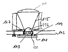
[0081] Figure 1 illustrates a mounting assembly according to an embodiment of
the
present invention. The mounting assembly comprises one or more light-emitting
elements 103 which are attached to a metallized and patterned substrate 101 to
allow for
electrical connectivity of the light-emitting elements 103. The substrate can
be made of
AIN, for example or other suitable material and would be known to a skilled
worker.
The substrate is removably attached to a FR4 carrier 102. This removable
attachment
may be provide by solder reflow for example or other suitable attachment
technique.
T'he carrier 102 has a through hole opening for receiving the one or more
light-emitting
elements.
16
CA 02617314 2007-10-05
WO 2006/105644 PCT/CA2006/000500
[0082] A primary optical system is disposed on the substrate including a dome
lens
116, a wall surface 108 and encapsulation material 107. A secondary optical
system
comprises a hollow reflector 115 and a collimating lens 111. The primary and
secondary optical systems are configured to extract light emitted by the one
or more
light-emitting elements under operating conditions and collimate the light
beam and mix
light of different colours or emission spectra. An optical index matching
material 107
can be inserted in the cavity between the light-emitting elements 103, the
substrate 101
the wall surface 108 and the dome lens 116 to enhance light extraction from
the one or
more light-emitting elements 103. The secondary optical system can be
removably
attached to the carrier 102, wherein the connection between the secondary
optical system
and the carrier can be provided by bolts, screws, friction or the like. The
carrier 102 can
be connected to the substrate 101 by solder or electrically conducting epoxy
by contact
pads 104.
[0083] In an alternate embodiment, the substrate 101 can be mechanically
clamped to
the carrier 102. A thermal management system, which is not illustrated, can be
thermally connected to the bottom of the substrate 101 thereby enabling
removal of heat
generated by the one or more light-emitting elements.
EXAMPLE 2:
[0084] Figure 2 illustrates a mounting assembly according to an embodiment of
the
present invention in which an insert 210 is used. The assembly comprises a
carrier 202
with an opening 208 there through for receiving one or more light-emitting
elements 203
mounted on the substrate 201 from one side and an insert 210 from an opposing
side. In
this embodiment the light-emitting elements and substrate are non-removably
mounted
to the carrier and thereby form a single unit. The insert 210 is positioned in
the opening
208 and can receive light emitted by the one or more light-emitting elements.
[0085] The insert can provide a shaped specular or diffuse reflective surface
facing the
one or more light-emitting elements and can provide beam shaping and colour
mixing of
the light emitted by the one or more light-emitting elements under operating
conditions.
It: is understood that the shape of the reflective surface associated with the
insert can be
adapted to optimize light extraction from a predetermined arrangement of the
one or
more light-emitting elements.
17
CA 02617314 2007-10-05
WO 2006/105644 PCT/CA2006/000500
[0086] The mounting assembly further comprises a primary optic 206, for
example a
dome lens, which can be attached to the insert 210 and it is understood that
the insert
can comprise further optical elements. The substrate 201 can be attached to
the carrier
202 with adhesives or solder and electrical connections to the carrier 202 can
be
achieved by solder or electrically conducting adhesive applied to designated
contact
pads 204. Optionally, the mechanical coupling between substrate and carrier
can be
enhanced by application of adhesive applied there between, for example.
[0087] An optical encapsulation material 207 can be inserted in the cavity
between the
insert 210, the primary optics 206, the one or more light-emitting elements
203 and the
substrate 201.
[0088] A thermal management system, which is not illustrated, can be thermally
connected to the bottom of the substrate 201 thereby enabling removal of heat
generated
by the light-emitting elements.
[0089] A secondary optical element 220 can be mounted on the carrier, wherein
the
secondary optical element can be provided for further manipulation of the
light emitted
by the light-emitting elements.
[0090] The insert 210 can be made of metal for example Al or it can be
fabricated
from plastics, ceramics or other suitable materials which would be obvious to
those
skilled in the art. The insert 210, when made of an electrically non-
conductive material,
can directly contact the substrate or can be spaced from the substrate.
[0091] In one embodiment, when the insert is manufactured from an electrically
conductive material, the insert 210 is positioned and configured such that it
does not
contact any circuit traces or other electrical contacts associated with either
the carrier or
the substrate. For example, the insert can be configured to leave an
appropriate amount
of space or can be mounted such that it rests on pads that electrically
isolate the insert
fi=om any electrical circuits or contacts associated with the substrate or the
carrier.
[0092] In one embodiment of the present invention, the insert can be designed
to aid
in the reduction of thermally induced differential strain between the carrier,
substrate,
for example.
18
CA 02617314 2007-10-05
WO 2006/105644 PCT/CA2006/000500
EXAMPLE 3:
[0093] Figure 3A illustrates a mounting assembly in which a lighting device
package
is removably mounted inferiorly to the carrier. The lighting device package is
further
illustrated in Figure 3B.
[0094] The lighting device package comprises a circumferential wall 310 which
is
attached to the substrate 301 together with one or more light-emitting
elements 303 and
a primary optical element 306. The interior of the lighting device package can
be filled
with an encapsulation material 307 and the substrate 301 can be manufactured
from
direct bonded copper or metallized A1N, for example, and can comprises
electrical
traces which are patterned on the top surface.
[0095] The wall structure 310 can be metallic and can also serve as an optical
element,
for example the wall structure can have a shaped reflective surface facing the
one or
more light-emitting elements 303. The wall structure can also be made of
plastic, for
example a liquid crystal polymer, ceramics or other compound materials. The
wall
structure can have any desired cross sectional shape and can be coated in
optically active
material such as phosphor.
[0096] The combination of the wall structure 310, substrate 301, and primary
optical
element 306 can seal the one or more light-emitting elements 303 from the
environment
and can be attached and electrically connected by the solder pads 304 to the
carrier 302.
The carrier comprises one or more openings there through for the positioning
of the
light-emitting package therein.
[0097] It is understood, that the carrier can be connected to the substrate by
separate
mechanical pads and electrical pads or that mechanical mounting functionality
and
electrical conductivity can be achieved through common pads and electrically
conductive epoxy or solder.
[0098] In one embodiment, one or more temperature sensors, optical sensors, or
other
sensors can be positioned proximate to the one or more light-emitting elements
on the
substrate or the carrier. The carrier may optionally have further electronic
devices,
electrical components or electrical circuits thereon which can provide
additional
functionality to the lighting device package.
19
CA 02617314 2007-10-05
WO 2006/105644 PCT/CA2006/000500
[0099] In one embodiment, the encapsulation material 307 can comprise
optically
active materials such as phosphors or quantum dots.
EXAMPLE 4:
[00100] Figure 4 illustrates a mounting assembly 400, wherein this example
illustrates
the thermal interface between the substrate and thermal management system
according
to one aspect of the present invention.
[00101] The mounting assembly comprises a carrier 402, an optical system, one
or
nlore electronic devices 430 attached to the carrier, a substrate 401 which
can have one
or more light-emitting elements 403 and one or more sensors 411. The optical
system
comprises a reflector 451, a transparent optical element 452, for example a
plano-
convex lens, a dome lens 406 and encapsulation material 407 injected into the
clearance
between the dome lens 406, reflective element 451, light-emitting element 403
and the
substrate 401.
1001021 The substrate can be soldered or glued to the carrier at a location of
a through
opening within the carrier. The optical system can be affixed to the carrier
by screws,
bolts, rivets, solder, adhesive, or any other mounting mechanism known in the
art.
[00103] A thermal management system, which is illustrated as a heat pipe 420
in this
example, is mounted to the cooling interface of the substrate 401. In order to
reduce the
mechanical stress on the cooling interface between the heat pipe and
substrate, a collar
421 can be attached to the carrier to support and guide the received heat
pipe. The collar
can comprise features that retain the heat pipe in a fixed position relative
to the
substrate. It is understood that the heat pipe can be permanently affixed by,
for example,
solder, adhesive, or it can be clamped, screwed, bolted or otherwise attached
to be non-
destructively detachable, wherein this connection can be configured to enhance
thermal
transfer between the substrate and the heat pipe. Thermal conductivity
enhancing
material can be for example a thermal paste, thermally conducting adhesive or
thermally
conducting film or solder provided at the interface between the substrate and
the heat
pipe. Optionally, the heat pipe can be replaced with a thermosyphon, or any
other
thermal management system as would be obvious to those skilled in the art.
CA 02617314 2007-10-05
WO 2006/105644 PCT/CA2006/000500
[00104] In one embodiment, additional electronic devices 430 can be mounted
onto the
carrier, wherein these electronic devices can be temperature sensors, optical
sensors,
controllers or control circuitry, or other electronic devices as would be
readily
understood by a worker skilled in the art.
EXAMPLE 5:
[00105] According to an embodiment of the present invention, Figure 5
illustrates
multiple mounting assemblies 510 which are thermally connected to a
horizontally
disposed thermal management system 520. The mounting assemblies 510 can be
configured as those described in relation to Figure 2.
[00106] The thermal management system can be in direct thermal contact with
one or
more substrate cooling interfaces of the mounting assemblies. The cooling
interfaces of
the mounting assemblies and the respective fitting surface areas of the
thermal
management system can be flat or have any other desired shape provided that
thermal
transmission there between achieves a desired threshold.
[00107] In one embodiment the thermal management system can be a heat pipe
wherein
the interfaces between a mounting assembly and the heat pipe are located
between the
ends of the heat pipe. The sections of the heat pipe that are in contact with
the substrate
can be flat to enhance heat extraction from the substrate.
1001081 In an alternate embodiment the thermal management system 520 can be a
flat
heat pipe, an embedded heat pipe system or a fluid cooled plate, for example.
EXAMPLE 6:
[00109] According to one embodiment of the present invention, Figure 6
illustrates a
mounting assembly in which the light-emitting elements 603 are mounted
directly onto a
thermal management system 620, for example a heat pipe, which is subsequently
inferiorly coupled to a carrier 602. The mounting surface of the thermal
management
system upon which the light-emitting elements are mounted comprises a
dielectric layer
and electrical traces thereon, thereby providing electrical connections to the
one or more
light-emitting elements and electrical isolation from the thermal management
system.
21
CA 02617314 2007-10-05
WO 2006/105644 PCT/CA2006/000500
[00110] The thermal management system can be mechanically and electrically
connected to a carrier 602 for supplying power and control signals to the
light-emitting
elements.
[00111] In one embodiment of the present invention, one or more electronic
devices
can be positioned on the side or on the end of the thermal management system
in
addition to the light-emitting elements mounted on the end thereof as
illustrated in
Figure 6.
[00112] In one embodiment, the thermal management system can be mounted to the
carrier on one side thereof. In an alternate embodiment, the thermal
management system
can be partially or fully inserted into a through opening formed within the
carrier.
EXAMPLE 7:
[00113] Figure 7 illustrates a mounting assembly according to another
embodiment of
the present invention, wherein the mounting assembly comprises an integrated
fluid lens
750, positioned in through openings in the carrier 702. The substrate 704 is
affixed to
the carrier 702 to form a sealed interface with the carrier 702. If required,
the inside
surfaces of the opening can be coated or otherwise hermetically sealed. The
side of the
carrier 702 opposing the substrate 704 can be environmentally sealed with a
window
760 of transparent material.
[00114] The fluid lens can be made of an electromagnetic field induced
refractive index
changing material, for example, a liquid crystal polymer whose refractive
index changes
in accordance with an applied electrical field. Alternately, the fluid lens is
configured to
change its focal length upon the application of an electric field thereto.
[00115] In one embodiment, the carrier can have one or more control electrodes
740
positioned on the inner surfaces of the openings. Each control electrode can
comprise a
single rotation-symmetric or rotation-asymmetric segment, for example in the
form of an
annular ring which can create a rotation-symmetric electrical field. Control
electrodes
for manipulation of the fluid lens 750 may be positioned inside, on the far
side, or on the
near side of the transparent window 760 or can be positioned on the far side
or on the
near side of the substrate 704.
22
CA 02617314 2007-10-05
WO 2006/105644 PCT/CA2006/000500
[00116] In one embodiment, the mounting assembly can further comprise one or
more
transparent dielectric liquids with different optical indices which can act as
a
controllable optical element, for example a variable focal-length optical
lens. The shape
of the interface between the dielectric fluids can be adapted to the
electrical field
conditions which can be controlled by applying voltage differences across a
combination
of one or more gates or control electrodes. The placement, design, and number
of gate
and control electrodes required to achieve a desired focal length control are
well known
to those skilled in the art. The control electrodes can also be part of a
housing element,
which is not shown, for example, an annular ring, which can be positioned in
the
opening.
[00117] It is understood, that the fluid lens 750 can be positioned freely by
combining
the variable a focal-length fluid lens with a lens-housing or it can be
combined with a
housing for an optical index matching material.
[00118] In one embodiment a window separates the opening in the carrier 702
into two
cavities, wherein one cavity receives the one or more light-emitting elements
and
encapsulation material and a second cavity contains the fluid lens. The window
can be
carrying gate or control electrodes for manipulation of the fluid lens.
[00119] It is understood that the gate electrodes can be manufactured out of
transparent
material such as indium tin oxide (ITO) wherever it is required that light can
propagate
through the electrode.
EXAMPLE 8:
[00120] Figure 8A illustrates a mounting assembly according to an embodiment
of the
present invention wherein one or more light-emitting elements 803 are directly
affixed
to a carrier 802 at designated openings. The mounting assembly further
comprises an
encapsulation material 807 applied into the opening, a primary optical element
806, a
secondary optical element 805. Optionally additional electronic devices 809
can be
attached to the carrier. A thermal management system 820 is thermally
connected to the
mounting assembly via a cooling interface of each of the one or more light-
emitting
elements.
23
CA 02617314 2007-10-05
WO 2006/105644 PCT/CA2006/000500
[00121] Figure 8B illustrates a light-emitting element according to an
embodiment of
the present invention which can be directly affixed to a carrier. The light-
emitting
element can comprise an emission window 813 and two electrical contact pads
815 and
816, wherein one is negative and the other is positive thereby enabling
activation of the
light-emitting element. In one embodiment, the emission window is designed to
have a
required size based on the overall size of the one or more light-emitting
elements,
thereby substantially maximizing the transmission of the light generated by
the one or
more light-emitting elements there through.
[00122] Figure 8C illustrates a semiconductor integrated circuit chip which
comprises
several integrated light-emitting elements (not shown) and light-emitting
windows 813.
Additionally the integrated circuit chip can comprise electrical contact pads
817 and 818
for control thereof, for example by interfacing to the carrier and a driver.
It is
understood that the integrated circuit chip can comprise further one or more
electronic
components, for example photosensors, thermal sensors or the like.
[00123] Figure 8D illustrates how one or more light-emitting elements 833 can
be
affixed to a carrier 839 which has electrical contacts on one side and one or
more
emission windows (not shown) for emitting light there through. The one or more
light-
emitting elements can have electrical connections on one or more sides and can
be
electrically connected to the carrier, for example, by using wire bonds 838.
[00124] Figure 8E illustrates a mounting assembly wherein the one or more
light-
emitting elements 843 have electrical contacts on two sides thereo~ The
carrier can
have one or more electrically conductive planes 847 and 845 which are
separated by an
electrically insulating plane 849, wherein these conductive planes provide
electrical
connections to the one or more light-emitting elements 843.
[00125] In one embodiment a first plane of the carrier provides electrical
connection to
a first contact of each of the one or more light-emitting elements located on
a first
surface and a second plane of the carrier can provide electrical connection to
a second
contact located on an opposing surface of the light-emitting element. For
example as
illustrated in Figure 8E, the first contact of the light-emitting element is
in direct contact
with the first plane 847 of the carrier and the second contact of the light-
emitting
element is wire bonded 848 to the second plane 845 of the carrier.
24
CA 02617314 2007-10-05
WO 2006/105644 PCT/CA2006/000500
[00126] In one embodiment, the one or more light-emitting elements can have a
patterned emission window to create homogeneous current injection. The pattern
can be
selected to enhance light extraction out of the one or more light-emitting
elements, for
example by using photonic crystals. It is also understood that the
metallization layer can
be manufactured from transparent material such as ITO.
[00127] In one embodiment, the semiconductor integrated circuit chip can
comprise
further integrated electronic components such as one or more of optical
sensors and
temperature sensors.
1001281 In one embodiment, the one or more light-emitting elements have
electrical
connections on one side thereof providing unobstructed access to an opposite
side of the
one or more light-emitting elements which can provide the cooling interfaces
which can
be directly connected to a thermal management system.
EXAMPLE 9:
1001291 Figure 9 illustrates a mounting assembly comprising a carrier 902 to
which one
or more light-emitting elements 903 are inferiorly mounted, according to
another
embodiment of the present invention. The mounting assembly is attached to a
two-stage
thermal management system. The thermal management system comprises a first
stage
923 and a second stage 925 cooling system. The first stage cooling system 923
comprises a phase change cooler, for example a heat pipe system. The heat pipe
system
is thermally connected to a second stage cooling system 925 which can comprise
a
finned heat sink. It is readily understood that the first stage and second
stage cooling
systems can comprise any combination of thermal management systems as would be
known to a worker skilled in the art, provided that this combination of
thermal
management systems would provide the desired heat dissipation of the heat
generated by
the one or more light-emitting elements.
[00130] In one embodiment, the first stage cooling system 923 can be formed
wherein
the carrier 902 and the one or more light-emitting elements 903 are
hermitically sealed
within a housing 910 to create a cavity. A wicking material 905 can be
provided on the
walls of the carrier and the cooling interface of the one or more light-
emitting elements
within the cavity. The cavity is charged with an evaporative fluid thereby
forming a heat
CA 02617314 2007-10-05
WO 2006/105644 PCT/CA2006/000500
pipe in which the one or more light-emitting elements form a portion of the
wall
structure.
[00131] In an alternate embodiment, the cavity can being filled with a highly
thermally
conductive fluid that transports heat by convection and conduction away from
the one or
more light-emitting elements. In a further embodiment a coolant could flow
through the
cavity to remove the heat generated by the one or more light-emitting
elements. In
another embodiment, the one or more light-emitting elements within the cavity
can be
cooled via spray cooling.
EXAMPLE 10:
[00132] Figure 10 illustrates a carrier 1002 wherein openings within the
carrier are not
provided according to one aspect of the invention. In this embodiment, the
carrier is
formed from a transparent material for example plastic or glass. The carrier
can
comprise one or more textured or otherwise structured surfaces 1007 providing
optical
manipulation of the light emitted by the one or more light-emitting elements
1003
inferiorly mounted onto the carrier 1002 by substrate 1001.
[00133] The textured or structured surfaces 1007 integral to the carrier can
provide
optical functionality and can assist in the extraction and beam shaping of
light emitted
by the one or more light-emitting elements under operating conditions. The
structured
surfaces can comprise for example one or more optical elements including dome
lenses,
lenticular arrays, diffractive optics, a holographic diffuser or any other
optical element
known to a skilled worker in the art.
[00134] In one embodiment, a pocket 1006 for receiving the light-emitting
elements
1003 is formed within the carrier 1002 at a position proximal to the light-
emitting
elements. Additionally encapsulation material can be inserted in the pocket
between
substrate 1001, light-emitting elements 1003 and carrier 1002.
[00135] In one embodiment, the carrier can have conductive traces disposed
thereon
that can provide electrical connection for the one or more light-emitting
elements to a
source of power or other devices which can be affixed to the carrier.
26
CA 02617314 2007-10-05
WO 2006/105644 PCT/CA2006/000500
1001361 Optionally the carrier can have secondary optical elements positioned
relative
to it or attached to it which can be located on the surface opposing or the
interface facing
the side of the one or more light-emitting elements. These optical elements
can be for
example, refractive or reflective elements or other desired optical elements
as would be
readily understood.
EXAMPLE 11:
[00137] Figure 11 illustrates a mounting assembly according to one embodiment
of the
present invention. The mounting assembly comprises a thermally conductive
substrate
1018, to which is thermally connected one or more light-emitting elements
1005. The
mounting assembly further comprises a primary optical element 1012 enclosing
the one
or more light-emitting elements 1005, wherein the space between the one or
more light-
emitting elements and the primary optical element 1012 is filled with an
encapsulation
material 1016, for example an optical silicone. The encapsulation material can
have an
index of refraction as close as possible to the light-emitting elements to
enhance light
extraction. Typically the refractive index of commercially available silicones
for this
type of application is in the order of about 1.4 to 1.6. The primary optical
element 1012
can be mounted directly onto the substrate 1018 using an adhesive such as
silicone or a
thermally or UV curable epoxy or other adhesive known to a worker skilled in
the art.
In an alternate embodiment, the primary optical element can be held in
position through
adhesion with the encapsulation material 1016. The primary optical element
comprises
an attachment site 1020, which can increase the bond line between the primary
optical
element and the substrate.
[00138] The mounting assembly is subsequently aligned with an opening 1014
within
the carrier 1010, wherein the substrate is coupled inferiorly to the carrier.
In this manner
the light emitted by the one or more light-emitting elements associated with
the
mounting assembly can pass through the opening formed within the carrier.
[00139] In one embodiment, electrical traces can be disposed on the substrate
to
provide electrical connection to the light-emitting elements. Electrical pads
on the
substrate can provide the electrical and mechanical interface and can
correlate to
electrical pads provided on the carrier. The substrate can be aligned and
oriented and
then soldered in place to achieve mechanical and electrical connection between
the
27
CA 02617314 2007-10-05
WO 2006/105644 PCT/CA2006/000500
substrate and the carrier. In one embodiment, further adhesive application can
strengthen this mechanical connection between the carrier and substrate.
[00140] In one embodiment, additional components such as thermal sensors or
optical
sensors to sample the optical flux can also be mounted on the substrate.
[00141] Figure 12 illustrates a secondary optical element 1020 interfaced to
the
mounting assembly illustrated in Figure 11. Provisions, for example indexing
features
in the carrier can allow the secondary optical element, which may have a
highly
reflective inner surface to be inserted into the clearing within the opening
in the carrier
and intimately mate with the primary optical element. In this manner about a
maximum
amount of the light generated by the light-emitting elements can be extracted
with about
a minimal aperture size. Furthermore the carrier can serve as an indexing
feature in both
lateral and vertical directions in order to achieve accurate placement of the
secondary
optical element and in order to aid in the avoidance of damage to the primary
optical
element and substrate assembly.
[00142] A thermal management system 1030, in this example a heat pipe,
interfaces to
the cooling interface of the substrate. The thermal connection between thermal
management system and substrate can be achieved by soldering the heat pipe and
substrate together which may require a metallization layer on the thermal
interface of the
substrate. Alternately, a thermal epoxy, thermal paste or thermal interface
film can be
used to enhance the thermal contact between the cooling interface of the
substrate and
the thermal management system 1030.
[00143] It is obvious that the foregoing embodiments of the invention are
exemplary
and can be varied in many ways. Such present or future variations are not to
be regarded
as a departure from the spirit and scope of the invention, and all such
modifications as
would be obvious to one skilled in the art are intended to be included within
the scope of
the following claims.
28