Note: Descriptions are shown in the official language in which they were submitted.
CA 02617385 2008-02-06
. o "
SPECIFICATION
MAGNETIC SENSOR, AND METHOD OF COMPENSATING
TEMPERATURE-DEPENDENT CHARACTERISTIC OF MAGNETIC
SENSOR
TECHNICAL FIELD
The present invention relates to a magnetic sensor utilizing a
magnetoresistive element.
This application is divided out of parent application serial number
2,507,819 filed on November 29, 2002.
BACKGROUND ART
There has hitherto been known a magnetic sensor which utilizes a
magnetoresistive element, such as a ferromagnetic magnetoresistive
element (MR element), a giant magnetoresistive element (GMR element) or
a tunnel magnetoresistive element (TMR element), as a magnetic field
detecting element, and which, on the basis of a resistance value of the
magnetoresistive element, generates an output value according to an
external magnetic field acting on the magnetoresistive element.
The resistance value of a magnetoresistive element is dependent on
temperature. Therefore, even when under a magnetic field of fixed
magnitude, output value of the magnetic sensor varies with the temperature
of the magnetoresistive element. Consequently, compensating this
temperature dependence is an essential requirement for detecting (the
magnitude of) a magnetic field with high precision.
A magnetic sensor apparatus described in Japanese Patent
Application Laid-open (kokai) No. H06-77558 attains such compensation by
1
CA 02617385 2008-02-06
means of a temperature sensor disposed adjacent to a magnetoresistive
element. A relation between voltage, serving as an output value of the
magnetic sensor, and temperature (temperature-dependent characteristic) is
measured in advance and stored in a memory. Then, on the basis of an
actual temperature detected by the temperature sensor and the relation
stored in the memory, a reference voltage is determined, and a difference
between an actual voltage output by the magnetic sensor and the
determined reference voltage is amplified and output to thereby compensate
the temperature-dependent characteristic of the magnetic sensor.
Meanwhile, the output value of a high sensitive magnetic sensor
varies under an influence of geomagnetism, and geomagnetism varies with
time. Consequently, the temperature-dependent characteristic stored in
the memory of the above-mentioned magnetic sensor apparatus must to be
measured within a predetermined short period of time in which
geomagnetism is ensured not to change; and during the above-described
measurement the magnetoresistive element must be heated or cooled within
a short period of time.
However, if the above-mentioned magnetoresistive element is
heated by an ordinary heating/cooling apparatus, not only the
magnetoresistive element, but the entire magnetic sensor, including a
substrate of the magnetoresistive element, is heated/cooled. Therefore,
heating/cooling time would be long due to the large heat capacity of the
magnetic sensor, and consequently geomagnetism would change during
measurement of the temperature dependence. As a result, a problem
would arise, in that the reliability of the temperature-dependent
characteristic stored in the memory would be lowered, and consequently
2
CA 02617385 2008-02-06
precise compensation of the temperature-dependent characteristic would be
impossible. Although one feasible solution is to measure the
temperature-dependent characteristic under an environment free from the
influence of geomagnetism, an apparatus (magnetic field canceller) for
establishing such environment is extremely expensive, thereby introducing
another problem of increasing the manufacturing cost of the magnetic
sensor.
Accordingly, an object of the present invention is to provide a
magnetic sensor, which is capable of measuring a temperature-dependent
characteristic inexpensively, within a short period of time, and with
precision,
and to provide a method for precisely compensating a
temperature-dependent characteristic of a magnetic sensor.
Another object of the present invention is to provide a single-chip
magnetic sensor which can generate an output signal of the magnetic
sensor without using a connecting wire; e.g., an Au wire for connecting the
magnetic sensor to external parts (for instance an external circuit).
Still another object of the present invention is to provide a magnetic
sensor in which external noise exerts substantially no influence on a control
circuit section which performs various operations such as generation of an
output signal on the basis of a change in resistance of a magnetoresistive
element, obtainment of data regarding the temperature characteristic of the
magnetoresistive element, initialization of the magnetization of the free
layer
of the magnetoresistive element, and application of an external magnetic
field to the magnetoresistive element for testing the performance of the
magnetoresistive element.
A further object of the present invention is to provide a magnetic
3
CA 02617385 2008-02-06
sensor having a structure suitable for fixing magnetization of pinned layers
of a plurality of magnetoresistive elements in the same direction easily and
reliably.
DISCLOSURE OF THE INVENTION
The invention of the parent application provides a magnetic sensor which
comprises a plurality of magnetoresistive elements formed on an upper surface
of
a layer superposed on a substrate, and a plurality of heat generating elements
adapted to generate heat when electrically energized, and which, on the
basis of resistance values of the plurality of magnetoresistive elements,
generates an output value corresponding to an external magnetic field
acting on the magnetoresistive elements, wherein the plurality of heat
generating elements are arranged and configured in such a way that, when
each of the plurality of heat generating elements generates a quantity of
heat approximately equal to the quantitv of heat aenerated bv anv of the
remaining heat generating elements in order to obtain data regarding
temperature characteristic of the magnetic sensor, the temperatures of the
plurality magnetoresistive elements become approximately equal to one
another, and the temperature of the upper surface of the layer on which the
plurality of magnetoresistive elements are formed becomes non-uniform
(uneven), and configured in such a way that each of the plurality of heat
generating elements does not generates any heat when the magnetic
sensor is used to measure the external magnetic field in a usual operation
mode, the temperatures of said plurality magnetoresistive elements become
equal to the temperature of the magnetic sensor. Examples of the
magnetoresistive elements include MR elements, GMR elements, and TMR
elements.
According to one aspect of the present application there is provided a
magnet sensor comprising a single substrate, a plurality of magnetoresistive
elements which are identical in magnetic field detecting direction, a wiring
section
bridge-interconnecting said plurality of magnetoresistive elements for
constituting
a bridge circuit to detect an external magnetic field in the magnetic field
detecting
4
CA 02617385 2008-02-06
direction, and a control circuit section for obtaining via said wiring section
a
physical quantity determined on the basis of resistance values of said
plurality of
magnetoresistive elements and processing the physical quantity so as to
generate
an output signal to be output to the outside, wherein said magnetic sensor has
a
plurality of layers superposed on said substrate; said magnetoresistive
elements
are formed on an upper surface of one of said plurality of layers; said wiring
section and said control circuit section are formed in said substrate and said
plurality of layers; and said magnetoresistive elements, said wiring section,
and
said control circuit section are interconnected in said plurality of layers by
a
connection section formed of a conductive substance and extending along a
direction intersecting layer surfaces of said layers.
According to another aspect of the present invention there is provided a
magnetic sensor comprising a substrate, a plurality of magnetoresistive
elements
disposed at an upper portion of said substrate, a wiring section disposed at
the
upper portion of said substrate and interconnecting said plurality of
magnetoresistive elements, and a control circuit section for obtaining via
said
wiring section a physical quantity determined on the basis of resistance
values of
said plurality of magnetoresistive elements and processing the physical
quantity
so as to generate an output signal to be output to the outside, wherein said
plurality of magnetoresistive elements are disposed at a peripheral portion of
said
substrate; said wiring section is disposed so as to form substantially a
closed
curve; and said control circuit section is disposed substantially inside said
closed
cu rve.
By virtue of the above-described arrangement and configuration,
when obtaining data regarding temperature characteristic of the magnetic
sensor, the entire magnetic sensor including the substrate is not heated to
the same temperature; and the plurality of magnetoresistive elements are
heated to approximately the same temperature (a temperature different from
the substrate temperature). Thus, it becomes possible to shorten the
period of
4a
CA 02617385 2008-02-06
time required for heating/cooling the magnetoresistive elements, so that the
temperature-dependent characteristics of the magnetoresistive elements
can be measured within a period of time in which the same geomagnetism
acts on the magnetoresistive elements.
In this case, the plurality of magnetoresistive elements may be
arranged to form a plurality of island-like element groups, each including a
plurality of magnetoresistive elements which are identical in magnetic field
detecting direction and arranged adjacent to each other on the upper
surface of the layer; and the heat generating elements may be formed such
that one is located above or beneath each element group. In this case,
because the heating members can heat mainly the magnetoresistive
elements, the period of time required for heating/cooling can be further
shortened.
Preferably, each of the heat generating elements assumes the form
of a coil (heating coil) capable of applying to the magnetoresistive elements
formed above or beneath the heat generating element a magnetic field in a
direction approximately identical with or approximately perpendicular to the
magnetic field detecting direction of the magnetoresistive elements. In this
case, the magnetic field whose direction is approximately identical with the
magnetic field detecting direction of the magneto resistive elements can be
used as a test magnetic field for determining whether or not the magnetic
sensor properly detects a magnetic field; and the magnetic field whose
direction is approximately perpendicular to the magnetic field detecting
direction of the magnetoresistive elements can be used as, for example, a
magnetic field dedicated to initialization of the free layers of the
magnetoresistive elements.
CA 02617385 2008-02-06
By virtue of this preferable structure, because the heat generating
element (heating coil) can serve also as a coil (test coil or initialization
coil)
for generating a magnetic field whose direction is approximately identical
with or approximately perpendicular to the magnetic field detecting direction
of the magnetoresistive element, it becomes possible to minimize the cost of
the magnetic sensor as a result of shortening the manufacturing process
and reducing the number of masks used in the manufacturing process.
Further, when this coil is electrically energized, measurement of the
temperature-dependent characteristic of the magnetic sensor, a portion or
entirety of testing of the magnetic sensor, and a portion or entirety of
initialization of the magnetic sensor can be carried out simultaneously;
therefore, the manufacturing (test) period of time can be shortened, thereby
reducing manufacturing cost.
The present invention also provides a magnetic sensor which
comprises a plurality of magnetoresistive elements formed on an upper
surface of a layer superposed on a substrate, and a single heat generating
element for generating heat when electrically energized, and which
generates an output value corresponding to an external magnetic field
acting on the magnetoresistive elements, on the basis of resistance values
of the plurality of magnetoresistive elements, wherein the heat generating
element is arranged and configured in such a manner that the temperatures
of the plurality of magnetoresistive elements become approximately equal to
one another, and that the temperature of the upper surface of the layer on
which the plurality of magnetoresistive elements are formed becomes
nonuniform.
By virtue of this alternative configuration as well, the entire magnetic
6
CA 02617385 2008-02-06
sensor including the substrate is not heated to the same temperature; and
the plurality of magnetoresistive elements are heated to approximately the
same temperature (a temperature different from the substrate temperature).
Thus, it becomes possible to shorten the period of time required for
heating/cooling the magnetoresistive elements, so that the
temperature-dependent characteristics of the magnetoresistive elements
can be measured within a period of time in which the same geomagnetism
acts on the magnetoresistive elements.
In this case, the heat generating element and the plurality of
magnetoresistive elements may be configured in such a manner that the
quantity of heat to be propagated from the heat generating element to an
arbitrary one of the plurality of magnetoresistive elements becomes
approximately identical with the quantity of heat to be propagated from the
heat generating element to one of the remaining magnetoresistive elements.
The heat generating element and the plurality of magnetoresistive
elements may be configured in such a manner that a relative positional
relation between the heat generating element and an arbitrary one of the
plurality of magnetoresistive elements becomes approximately identical with
the relative positional relation between the heat generating element and one
of the remaining magnetoresistive elements.
Preferably, the plurality of magnetoresistive elements are arranged
separately in four islands spaced from one another on the upper surface of
the layer superposed on the substrate, and are formed in such a way that,
when the plurality of magnetoresistive elements are rotated within a plane
parallel to the upper surface of the layer through 90 about a centroid of a
quadrilateral figure defined by four straight lines each interconnecting
7
CA 02617385 2008-02-06
approximate centers of adjacent islands, an arbitrary one of the islands
becomes substantially aligned with a position which before the angular
movement through 90 had been occupied by another island that is adjacent
to the arbitrary island in the direction of the angular movement.
Further, the magnetic sensor having any of the above-mentioned
features may further comprise a temperature detecting section that outputs,
as a detection temperature, a temperature having a constant correlation with
the temperature of at least one of the plurality of magnetoresistive elements
when the temperatures of the plurality of magnetoresistive elements become
approximately equal to one another, and the temperature of the upper
surface of the layer on which the plurality of magnetoresistive elements are
formed becomes nonuniform.
As described above, the magnetoresistive elements are heated to
approximately the same temperature as a result of heat radiation of the heat
generating element(s). Therefore, in the case in which the temperature
detecting section has a constant correlation with at least one of the
plurality
of magnetoresistive elements in terms of temperature, the temperature
detecting section can detect the temperatures of substantially all the
magnetoresistive elements of the same configuration. Therefore,
according to the above-mentioned configuration, the temperature detecting
section is not required to be increased in number, and thus the cost of the
magnetic sensor can be reduced.
Further, in the magnetic sensor including the above-mentioned
temperature detecting section, preferably, the plurality of magnetoresistive
elements are interconnected in such a way that, among the
magnetoresistive elements, elements identical in magnetic field detecting
8
CA 02617385 2008-02-06
direction constitute a bridge circuit in order to generate an output value
corresponding to said external magnetic field; and the magnetic sensor
further comprises a memory, and temperature-dependent characteristic
writing means for writing into the memory a value that is determined on the
basis of "data representing a first temperature of the magnetoresistive
elements, determined on the basis of the detection temperature output from
the temperature detecting section, and a first output value output from the
magnetic sensor at the first temperature," and "data representing a second
temperature of the magnetoresistive elements, different from the first
temperature and determined on the basis of the detection temperature
output from the temperature detecting section, and a second output value
output from the magnetic sensor at the second temperature," the value to be
written into the memory corresponding to a ratio of a difference between the
first and second output values to a difference between the first and second
temperatures.
The temperature-dependent characteristic of a magnetic sensor in
which a plurality of magnetoresistive elements constitutes a bridge circuit
(full-bridge circuit) is such that the output of the magnetic sensor changes
in
proportion to the variation in temperature of the magnetoresistive element.
Therefore, if a value corresponding to the above-described "ratio" (i.e.,
variation in output value of the magnetic sensor with respect to variation in
temperature of the magnetoresistive element), which value may be the ratio
itself, the inverse of the ratio, etc., is stored in advance in a memory, an
electronic apparatus can obtain data of the temperature-dependent
characteristic of the magnetic sensor by reading the "ratio" from the memory
after the magnetic sensor is mounted in the electronic apparatus.
9
CA 02617385 2008-02-06
Therefore, the data can be used to compensate the temperature-dependent
characteristic of the magnetic sensor.
In other words, data regarding the temperature-dependent
characteristic of each magnetic sensor can be held in the magnetic sensor
through a simple operation of storing a value corresponding to the
above-described "ratio" in the memory of the magnetic sensor. Therefore,
it is possible to minimize the capacity of the memory in which data of the
temperature-dependent characteristic of the magnetic sensor is to be stored,
thereby lowering the cost of the magnetic sensor.
The present invention further provides a method of compensating a
temperature-dependent characteristic of a magnetic sensor which includes a
magnetoresistive element whose resistance varies according to an external
magnetic field, a first memory, a temperature detecting section for
outputting,
as a detection temperature, a temperature having a constant correlation with
the temperature of the magnetoresistive element, and a heat generating
element for generating heat when electrically energized; and which
generates an output value corresponding to the external magnetic field on
the basis of a resistance value of the magnetoresistive element; the
magnetic sensor being adapted for incorporation in an electronic apparatus
which includes a permanent magnet component, a casing, and a second
memory, wherein the casing accommodates the magnetic sensor, the
permanent magnet component, and the second memory; the method
comprising the steps of: obtaining a first temperature of said
magnetoresistive element on the basis of the detection temperature output
from said temperature detecting section, obtaining a first output value output
from said magnetic sensor at the first temperature, before said magnetic
CA 02617385 2008-02-06
sensor is accommodated in said casing; obtaining a second temperature of
said magnetoresistive element on the basis of the detection temperature
output from said temperature detecting section after the electrically
energized state of said heat generating element is changed, and obtaining a
second output value output from said magnetic sensor at the second
temperature, before said magnetic sensor is accommodated in said casing;
storing into the first memory a value corresponding to a ratio of a difference
between the first and second output values to a difference between the first
and second temperatures; storing into the second memory, as reference
data, an offset value of the output value of the magnetic sensor and a
detection temperature output from the temperature detecting section after
the magnetic sensor is accommodated in the casing together with the
permanent magnet component; and thereafter, correcting the output value of
the magnetic sensor on the basis of the value corresponding to the ratio
stored in the first memory, the reference data stored in the second memory,
and the detection temperature output from the temperature detecting
section.
By this method, data to obtain a value corresponding to the
above-described "ratio," serving as data representing the
temperature-dependent characteristic of the magnetic sensor, is obtained
and/or stored into the first memory in a stage in which the magnetic sensor
has not yet been mounted in an electronic apparatus. Then, after the
magnetic sensor is accommodated in the casing together with the
permanent magnet component and the second memory, an offset value of
the output value of the magnetic sensor and a temperature detected by the
temperature detecting section when the offset value is obtained are stored
11
CA 02617385 2008-02-06
into the second memory. Subsequently, the actual output value of the
magnetic sensor is corrected on the basis of a difference between an actual
temperature detected by the temperature detecting section and the
temperature stored in the second memory, the value corresponding to the
"ratio" and stored in the first memory, and the offset value stored in the
second memory.
This method will be described by use of a specific example. The
difference between an actual temperature detected by the temperature
detection section and the temperature stored in the second memory is
multiplied by the "ratio" stored in the first memory so as to obtain an amount
of change in offset value resulting from variation in temperature of the
magnetic sensor. Subsequently, the offset value stored in the second
memory is added to the amount of change in offset value so as to obtain an
after-temperature-change offset value; and a difference between the actual
output value of the magnetic sensor and the after-temperature-change offset
value is used as a value corresponding to an external magnetic field to be
detected.
Thus, according to the temperature-dependent characteristic
compensating method of the present invention, a value according to the
above-described "ratio" is measured in a stage in which the magnetic sensor
has not yet been mounted in an electronic apparatus, and stored into the
first memory. Therefore, the magnetic sensor itself can possess data
representing the temperature-dependent characteristic of the magnetic
sensor. Further, because the offset value and the detection temperature
output from the temperature detecting section are stored into the second
memory after the magnetic sensor is mounted in the casing of an electronic
12
CA 02617385 2008-02-06
apparatus together with the permanent magnet component, there is no need
to store into the first memory the offset value of the magnetic sensor itself
and the detection temperature output from the temperature detection section
when the offset value is obtained. Therefore, the storage capacity of the
first memory can be minimized to thereby lower the cost of the magnetic
sensor. Moreover, since two types of offsets of the magnetic sensor; i.e.,
an offset (reference shift) of the magnetic sensor itself stemming from the
individual difference (difference in resistance value) of the magnetoresistive
element and an offset (reference shift) attributable to a leakage magnetic
field from the permanent magnet component, can be obtained
simultaneously after the magnetic sensor is mounted in the casing, there is
no need to obtain the offset value twice. Thus, according to the present
invention, the temperature-dependent characteristic of the magnetic sensor
can be compensated in a simple manner.
The present invention also provides a magnet sensor comprising a
single substrate, a plurality of magnetoresistive elements, a wiring section
bridge-interconnecting the plurality of magnetoresistive elements, and a
control circuit section for obtaining via the wiring section a physical
quantity
determined on the basis of resistance values of the plurality of
magnetoresistive elements and processing the physical quantity so as to
generate an output signal to be output to the outside, wherein the magnetic
sensor further includes a plurality of layers superposed on the substrate; the
magnetoresistive elements are formed on an upper surface of one of the
plurality of layers; the wiring section and the control circuit section are
formed in the substrate and the plurality of layers; and the magnetoresistive
elements, the wiring section, and the control circuit section are
13
CA 02617385 2008-02-06
interconnected in the plurality of layers by a connection section formed of a
conductive substance and extending along a direction intersecting layer
surfaces of the layers.
By virtue of this structure, the magnetoresistive elements, the wiring
section, and the control circuit section are interconnected within the
plurality
of layers, without crossing, by the connection section which is formed of a
conductive substance and extends along a direction intersecting the layer
surfaces of the layers. Thus, there is provided a single-chip magnetic
sensor which can generate an output signal of the magnetic sensor, without
use of a connecting wire, unlike a magnetic sensor in which the chip is
divided into a chip which carries magnetoresistive elements and a chip
which carries a control circuit section, etc, and in which a connecting wire
is
used to connect the chips.
Further, the present invention provides a magnetic sensor
comprising a substrate, a plurality of magnetoresistive elements disposed at
an upper portion of the substrate, a wiring section disposed at the upper
portion of the substrate and interconnecting the plurality of magnetoresistive
elements, and a control circuit section for obtaining via the wiring section a
physical quantity determined on the basis of resistance values of the
plurality of magnetoresistive elements and processing the physical quantity
so as to generate an.output signal to be output to the outside, wherein the
plurality of magnetoresistive elements are disposed at a peripheral portion
of the substrate as viewed in plan; the wiring section is disposed so as to
form substantially a closed curve as viewed in plan; and the control circuit
section is disposed substantially inside the closed curve as viewed in plan.
By virtue of this configuration, the control circuit section for
14
CA 02617385 2008-02-06
performing, for example, the generation of an output signal on the basis of a
change in resistance of the magnetoresistive element or the obtaining of
data of temperature characteristic of the magnetoresistive element, can be
disposed within a compact space at the central portion of the substrate as
viewed in plan. Therefore, the length of wiring in the control circuit section
is shortened, and hence external noise can hardly be superposed on the
wiring. As a result, there is provided a magnetic sensor which is hardly
affected by external noise and is highly reliable.
Further, the present invention provides a magnetic sensor
comprising a single substrate and a plurality of element groups, each
element group including a pair of magnetoresistive elements which are
identical in terms of magnetization direction of a pinned layer, at least two
of
the element groups being perpendicular in terms of magnetization direction
of said pinned layer to each other, wherein each of the plurality of element
groups is disposed on the substrate in such a way that the magnetization
direction of the pinned layer of each element group is substantially parallel
to a direction in which a distance from a centroid (center) of the substrate
increases, and such that the pair of magnetoresistive elements are disposed
adjacent to each other_~
The sensor above is a magnetic sensor comprising a single
substrate and a plurality of element groups, each element group including a
pair of magnetoresistive elements which are identical in terms of
magnetization direction of a pinned layer, at least two of the element groups
being perpendicular in terms of magnetization direction of a free layer of
said magnetoresistive element to each other when an external magnetic
field is not applied, wherein each of said plurality of element groups is
disposed on said substrate in such a way that, when the external magnetic
field is not applied, the magnetization direction of said free layer of each
element group is substantially perpendicular to a direction in which a
distance from centroid of said substrate increases, and such that said pair of
magnetoresistive elements are disposed adjacent to each other.
fixed, a magnetic field of stabilized direction and magnitude must be
continually applied to the magnetoresistive element. At this time, at two
neighboring points on the same line of magnetic force, the magnetic field
assumes approximately the same magnitude in approximately the same
direction. Further, in a magnetic sensor, on many occasions, in order to
improve the temperature characteristic etc. of the magnetic sensor, a
plurality of element groups each including a pair of magnetoresistive
CA 02617385 2008-02-06
elements of identical pinned-layer magnetization direction (i.e., of identical
magnetic field detecting direction) are provided, and these magnetoresistive
elements are bridge-interconnected.
Therefore, in the case of the magnetic sensor configured in the
above-described manner in which each of the plurality of element groups is
disposed at an upper portion of the substrate such that the above-described
pinned-layer magnetization direction is substantially parallel to the
direction
in which the distance from the centroid (center) of the substrate increases,
as viewed in plan, and such that the pair of magnetoresistive elements are
disposed adjacent to each other in that direction, when a magnetic field
directed from the centroid (center) of the substrate toward its periphery acts
on the magnetic sensor, magnetization of the pinned layer of the
magnetoresistive elements can be fixed, by virtue of the magnetic field
having the same magnitude and the same direction. As a result, the
pinned layers of the magnetoresistive elements can be magnetized in the
same direction easily and reliably.
BRIEF DESCRIPTION OF THE DRAWINGS
FIG. 1 is a schematic plan view of a magnetic sensor according to a
first embodiment of the present invention;
FIG. 2 is a schematic plan view of a portion of the magnetic sensor
of FIG. 1, showing an electrical wiring state of the magnetic sensor;
FIG. 3 is a schematic cross-sectional view of a portion of the
magnetic sensor of FIG. 1, taken along a predetermined plane perpendicular
to the surfaces of individual layers constituting the magnetic sensor;
FIG. 4 is a graph showing variations in the resistance value of a
16
CA 02617385 2008-02-06
GMR element of FIG. 1 with respect to an external magnetic field;
FIG. 5 is a schematic plan view of a magnetic sensor according to a
modification of the first embodiment;
FIG. 6 is an enlarged plan view of a portion of the magnetic sensor of FIG.
1;
FIG. 7 is an equivalent circuit diagram of an X-axis magnetic sensor
of the magnetic sensor of FIG. 1;
FIG. 8 is a graph showing variations in the output voltage (output
signal) of the X-axis magnetic sensor constituting the magnetic sensor of
FIG. 1, with respect to an external magnetic field;
FIG. 9 is a front view of a cellular phone on which the magnetic
sensor of FIG. 1 is to be mounted;
FIG. 10 is a graph showing a temperature-dependent characteristic
of the X-axis magnetic sensor constituting the magnetic sensor of FIG. 1;
FIG. 11 is a graph showing a temperature-dependent characteristic
of a Y-axis magnetic sensor which constitutes a portion of the magnetic
sensor of FIG. 1;
FIG. 12 is a schematic plan view of the magnetic sensor of FIG. 1,
showing isothermal lines when heating coils of the magnetic sensor are
energized;
FIG. 13 is a graph showing a relation between the lapse of time from
electrical energization of the heating coils of the magnetic sensor of FIG. 1
and the variation in temperature of the GMR element;
FIG. 14 is a schematic plan view of a magnetic sensor according to
a second embodiment of the present invention;
FIG. 15 is a cross-sectional view of a portion of the magnetic sensor,
17
CA 02617385 2008-02-06
taken along 1-1 line in FIG. 14;
FIG. 16 is a schematic plan view of the magnetic sensor of FIG. 14,
showing isothermal lines when heating coils of the magnetic sensor are
electrically energized;
FIG. 17 is a schematic plan view of a magnetic sensor according to
a modification of the second embodiment of the present invention, showing
isothermal lines when heating coils of the magnetic sensor are electrically
energized; and
FIG. 18 is a schematic cross-sectional view of another modification
of the magnetic sensor according to the present invention.
BEST MODE FOR CARRYING OUT THE INVENTION
(First Embodiment)
Embodiments of a magnetic sensor according to the present
invention will now be described with reference to the accompanying
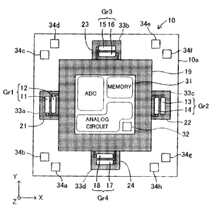
drawings. FIG. 1 is a schematic plan view of a magnetic sensor 10
according to a first embodiment; FIG 2 is a schematic plan view of a portion
of the magnetic sensor 10, showing the electrical wiring of the magnetic
sensor 10; and FIG. 3 is a schematic cross-sectional view of a portion of the
magnetic sensor shown in FIGS. 1 and 2, taken along a predetermined
plane perpendicular to the surfaces of individual layers constituting the
magnetic sensor 10.
The magnetic sensor 10 includes a substrate 10a which is formed of
Si3N4/Si, SiO2/Si, or quartz glass and which has an approximately square (or
rectangular) shape with sides extending along mutually perpendicular X-
and Y-axes and has a small thickness in a Z-axis direction perpendicular to
18
CA 02617385 2008-02-06
the X- and Y-axes; layers INS1 and S1-S3 superposed on the substrate 10a
and identical in shape with the substrate 10a as viewed in plan; a total of
eight GMR elements 11-18 formed on (an upper surface of) the layer S3 as
magnetoresistive elements; and a passivation layer PL formed as an
uppermost surface.
As shown in FIG. 1, the magnetic sensor 10 has a bridge wiring
section (connection wire section) 19 bridge-interconnecting the GMR
elements 11-14 and the GMR elements 15-18, respectively, to constitute
two full-bridge circuits; heating coils 21-24 serving as heating elements for
heating the GMR elements 11-18; a control circuit section (LSI) 31; a
temperature detecting section 32; test coils 33a-33d; and pads 34a-34h for
connecting the magnetic sensor 10 with external equipment via Au wires
bonded to the upper surfaces of the pads.
The GMR element 11 is called the first X-axis GMR element 11 and,
as shown in FIG. 1, is formed on the substrate 10a in the vicinity of the
approximate center of a left-hand side of the substrate 10a extending along
the Y-axis direction. The GMR element 12 is called the second X-axis
GMR element 12 and is disposed in the vicinity of the approximate center of
the left-hand side of the substrate 10a in such a manner that the second
X-axis GMR element 12 is located adjacent to (neighboring) the first X-axis
GMR element 11 at a position spaced a short distance in the positive X-axis
direction from the first X-axis GMR element 11.
The GMR element 13 is called the third X-axis GMR element 13 and
is formed on the substrate 10a in the vicinity of the approximate center of a
right-hand side of the substrate 10a extending along the Y-axis direction.
The GMR element 14 is called the fourth X-axis GMR element 14 and is
19
CA 02617385 2008-02-06
disposed in the vicinity of the approximate center of the right-hand side of
the substrate 10a in such a manner that the fourth X-axis GMR element 14
is located adjacent to (neighboring) the third X-axis GMR element 13 at a
position spaced a short distance in the negative X-axis direction from the
third X-axis GMR element 13.
The GMR element 15 is called the first Y-axis GMR element 15 and
is formed on the substrate 10a in the vicinity of the approximate center of
the upper side of the substrate 10a extending along the X-axis direction.
The GMR element 16 is called the second Y-axis GMR element 16 and is
disposed in the vicinity of the approximate center of the upper side of the
substrate 10a in such a manner that the second Y-axis GMR element 16 is
located adjacent to (neighboring) the first Y-axis GMR element 15 at a
position spaced a short distance in the negative Y-axis direction from the
first Y-axis GMR element 15.
The GMR element 17 is called the third Y-axis GMR element 17 and
is formed on the substrate 10a in the vicinity of the approximate center of
the lower side of the substrate 10a extending along the X-axis direction.
The GMR element 18 is called the fourth Y-axis GMR element 18 and is
disposed in the vicinity of the approximate center of the lower side of the
substrate 10a in such a manner that the fourth Y-axis GMR element 18 is
located adjacent to (neighboring) the third Y-axis GMR element 17 at a
position spaced a short distance in the positive Y-axis direction from the
third Y-axis GMR element 17.
A spin valve layer constituting each of the GMR elements 11-18
includes a free layer, a conductive spacer layer, a pin layer (fixed
magnetization layer), and a capping layer which are superposed (formed)
CA 02617385 2008-02-06
. . = ,
one over another on the upper surface of the layer S3 on the substrate 10a.
The magnetization direction of the free layer changes freely in accordance
with variation in the external magnetic field. The pin layer includes a
pinning layer and a pinned layer; the magnetization direction of the pinned
layer is fixed by the pinning layer and does not change with respect to the
external magnetic field except in a special case.
Each of the GMR elements 11-18 thereby assumes a resistance
value corresponding to an angle between the pinned-layer magnetization
direction and the free layer magnetization direction. Namely, each of the
GMR elements 11-18, as indicated by solid lines in the graph of FIG. 4,
assumes a resistance value which varies within the range of -Hc to +Hc
approximately in proportion to an external magnetic field varying in the
pinned-layer magnetization direction; and, as indicated by dotted lines,
assumes a resistance value which is approximately constant for an external
magnetic field varying in the direction perpendicular to the pinned-layer
magnetization direction. In other words, each of the GMR elements 11-18
is such that the pinned-layer magnetization direction is identical with-the
magnetic field detecting direction.
The pinned-layer magnetization direction of each of the GMR
elements 11 and 12 is the negative X direction. Namely, the first and
second X-axis GMR elements 11 and 12 form one element group Gr1 in
which a plurality of magnetoresistive elements which detect the magnitude
of a magnetic field in the same direction (in this case the X direction);
i.e.,
which have the same magnetic field detecting direction, are located adjacent
to one another in the form of an island on the layer S3 superposed on the
substrate 10a.
21
CA 02617385 2008-02-06
The pinned-layer magnetization direction of each of the GMR
elements 13 and 14 is the positive X direction. Namely, the third and
fourth X-axis GMR element 13 and 14 form another element group Gr2 in
which a plurality of magnetoresistive elements for detecting the magnitude
of a magnetic field in the same direction (in this case the X direction) are
located adjacent to one another in the form of an island on the layer S3
superposed on the substrate 10a.
The pinned-layer magnetization direction of each of the GMR
elements 15 and 16 is the positive Y direction. Namely, the first and
second Y-axis GMR elements 15 and 16 form still another element group
Gr3 in which a plurality of magnetoresistive elements for detecting the
magnitude of a magnetic field in the same direction (in this case the Y
direction) are located adjacent to one another in the form of an island on the
layer S3 superposed on the substrate 10a.
The pinned-layer magnetization direction of each of the GMR
elements 17 and 18 is the negative Y direction. Namely, the third and
fourth Y-axis GMR element 17 and 18 form a further element group Gr4 in
which a plurality of magnetoresistive elements for detecting the magnitude
of a magnetic field in the same direction (in this case the Y direction) are
located adjacent to one another in the form of an island on the layer S3
superposed on the substrate 10a.
Thus, the GMR elements 11-18 form four element groups (islands)
Gr1-Gr4 in which two neighboring magnetoresistive elements of each
element group are identical in terms of magnetic field detecting direction.
These element groups Gr1-Gr4 are disposed outside the approximate center
positions of the respective sides of a square (sides of the square bridge
22
CA 02617385 2008-02-06
wiring section 19 as viewed in plan) having sides along the X and Y
directions as viewed in plan, and are formed in such a way that, when an
arbitrary element group is angularly moved through 900 about a centroid of
the square (the center of the square; i.e., the intersection point of diagonal
lines of the square), the arbitrary element group becomes substantially
aligned with a position that before the angular movement through 90 had
been occupied by another, neighboring element group. In other words, the
plurality of GMR elements 11-18 are disposed in four spaced islands on the
upper surface of the layer S3 superposed on the substrate 10a, and are
formed in such a manner that, when the plurality of magnetoresistive
elements 11-18 are angularly moved in a plane parallel to the upper surface
of the layer S3 through 90 about the centroid GP of a quadrangle formed
by four straight lines interconnecting approximate centers of adjacent pair of
the islands, an arbitrary one of the islands becomes substantially aligned
with a position before the anguiar movement through 90 had been occupied
by another, neighboring island in the direction of the angular movement.
Namely, assuming not only that four straight lines (line segments); i.e., a
straight line interconnecting the approximately central portions of the
element groups Gr2 and Gr3, a straight line interconnecting the
approximately central portions of the element groups Gr3 and Gr1, a straight
line interconnecting the approximately central portions of the element
groups Gr1 and Gr4, and a straight line interconnecting the approximately
central portions of the element groups Gr4 and Gr2, are obtained, but also
that, when the element groups are angularly moved through 90 about the
centroid of a quadrangle formed by these line segments, each element
group becomes aligned with the position that before the angular movement
23
CA 02617385 2008-02-06
had been occupied by another, neighboring element group; namely, the
element group Gr2 becomes aligned with the former position of the element
group Gr3, the element group Gr3 becomes aligned with the former position
of the element group Gri, and so forth.
In the example shown in FIGS. 1 through 3, two GMR elements
constituting a single island (a single element group) are located adjacent to
each other in the direction from the center (centroid, which is aligned with
the above-mentioned centroid GP) of the substrate i Oa toward one side
(periphery) of the substrate 10a. Namely, each of the plurality of element
groups Gr1-Gr4 each including a pair of magnetoresistive elements of
identical magnetic field detecting direction is disposed at the upper portion
of the substrate 10a in such a way that the pinned-layer magnetization
directions of the magnetoresistive elements become substantially parallel to
the direction in which a distance from the centroid of the substrate 10a
increases, as viewed in plan, and such that the above-mentioned pair of
magnetoresistive elements are disposed adjacent to each other in the same
direction. Alternatively, as shown in FIG. 5, a pair of magnetoresistive
elements may be disposed adjacent to each other in the direction along one
side of the substrate 10a. However, according to the former arrangement,
because the GMR elements come closer to the centers of the respective
sides of the (square) substrate 10a as compared with the latter arrangement,
the characteristics of the elements can easily become uniform. Further, in
the case of the former, a magnetic field having the same magnitude in the
same direction can be easily applied to a pair of magnetoresistive elements
as compared with the latter case.
As exemplified in FIG. 6, which is an enlarged plan view of an area
24
CA 02617385 2008-02-06
in the vicinity of the GMR elements 11 and 12, the GMR elements 11-14 are
connected to the respective wires of the bridge wiring section 19, to thereby
constitute a bridge circuit (full-bridge connected) through the medium of the
bridge wiring section 19 as shown in an equivalent circuit diagram of FIG. 7,
thereby constituting the X-axis magnetic sensor whose magnetic field
detecting direction is the X direction. In FIG. 7, an arrow labeled in each
GMR element 11-14 indicates the pinned-layer magnetization direction of
the respective GMR element 11-14.
More specifically, the X-axis magnetic sensor is such that, when a
constant potential difference is applied between a junction Va between the
first and fourth X-axis GMR elements 11 and 14 and a junction Vb between
the third and second X-axis GMR elements 13 and 12, a potential difference
(Vc - Vd) between a junction Vc between the first and third X-axis GMR
elements 11 and 13 and a junction Vd between the second and fourth X-axis
GMR elements 12 and 14 is derived as a sensor output value Vxout. As a
result, the output voltage (physical quantity represented by voltage) of the
X-axis magnetic sensor changes approximately in proportion to the
magnitude of an external magnetic field within- the range of -Hc to +Hc,
which magnitude varies along the X-axis, as indicated by solid lines in FIG.
8; and remains at a constant value of approximately "0" for an external
magnetic field whose magnitude varies along the Y-axis.
Similar to the case of the GMR elements 11-14, the GMR elements
15-18 are connected to the respective wires of the bridge wiring section 19
to constitute a bridge circuit (full-bridge connected), thereby constituting
the
Y-axis magnetic sensor whose magnetic field detecting direction is the
Y-axis direction. Namely, the Y-axis magnetic sensor exhibits an output
CA 02617385 2008-02-06
- = .
voltage (physical quantity represented by voltage) Vyout which changes
approximately in proportion to the magnitude of an external magnetic field
within the range of -Hc to +Hc, which magnitude varies along the Y-axis;
and exhibits an output voltage of approximately "0" with respect to an
external magnetic field whose magnitude varies along the X-axis.
As shown in Fig. 1, the bridge wiring section 19 is formed at the
periphery of an approximate square area having sides along the X-axis and
Y-axis and located inside the GMR elements 11-18, as viewed in plan,
thereby constituting substantially a closed curve (including straight
portions).
As described in detail later, the bridge wiring section 19 is formed in the
layer S3 beneath the GMR elements 11-18.
As shown in FIGS. 1 and 3, heating coils 21-24 are embedded in the
layer S3, which functions as a wiring layer, to be located right beneath the
element groups Gr1-Gr4 (in the negative Z direction). The heating coiis
21-24 are approximately identical with each other in terms of shape and
positional relation with the corresponding element groups Gr1-Gr4.
Therefore, in the following description, only the heating coil 21 is described
in detail.
The heating coil 21 is a heat generating element formed of, for
example, aluminum thin film. When electrically energized, the heating coil
21 generates heats to thereby heat the first and second GMR elements 11
and 12 (element group Gr1). The heating coil 21 is formed in the layer S3
to face the lower surfaces of the magnetoresistive elements 11 and 12, to
thereby be disposed directly below the element group Gr1. Namely, as is
understood from FIG. 3, the heating coil 21 is embedded and formed in the
layer S3, among the insulating layer INS1 and the layers S1-S3 superposed
26
CA 02617385 2008-02-06
r ' =
one over another on the substrate 10a, on which layer the GMR elements
11-18 are formed (the uppermost layer S3 among the layers S1-S3 each
functioning as a wiring layer). In the present description, a layer
functioning as a wiring layer refers to wires, an interlayer insulating layer
between wires, and contact holes (including via-holes) for establishing
connection between wires.
Further, as shown in FIG. 6, the heating coil 21 is a so-called
double-spiral coil which is approximately rectangular in shape as viewed in
plan and which includes a pair of coiled conductors (i.e., a first conductor
21-1 having a coil center P1 and a second conductor 21-2 having a coil
center P2); the Y-direction length of the rectangular shape is approximately
two times the longitudinal length of the magnetoresistive element 11 (12),
and the X-direction length of the rectangular shape is approximately five
times the transverse (direction perpendicular to the longitudinal direction)
length of the magnetoresistive element 11 (12).
In addition, the first and second X-axis GMR elements 11 and 12 are
located between the two coil centers P1 and P2 as viewed in plan. Further,
portions of the first and second conductors 21-1 and 21-2 which overlap the
first and second X-axis GMR elements 11 and 12 (i.e., portions extending
directly under the first and second X-axis GMR elements 11 and 12) as
viewed in plan, extend linearly in parallel to each other in the X direction.
These straight portions of each conductor are adapted to carry a current of
the same flow direction and to thereby generate a magnetic field in the
Y-axis direction. Namely, the heating coil 21 is adapted to generate a
magnetic field in a direction that coincides with the longitudinal direction
of
the first and second X-axis GMR elements 11 and 12, and in the designed
27
CA 02617385 2008-02-06
R r =
direction (direction perpendicular to the fixed direction of magnetization of
the pinned layer) of magnetization of the free layer in the absence of
application of any external magnetic field.
As described above, the magnetic sensor 10 according to the first
embodiment is a magnetic sensor including the GMR elements
(magnetoresistive elements each including a free layer and a pin layer), and
equipped with the heating coils 21-24 which are disposed under (and
adjacent to) the free layer and adapted to stabilize (initialize) the
direction of
magnetization of the free layer in the absence of application of any external
magnetic field and which, when electrically energized under a
predetermined condition (e.g., before the start of detection of magnetism),
generates in the free layer a magnetic field (an initializing magnetic field)
having a predetermined direction (perpendicular to the pinned-layer
magnetization direction). Further, the heating coils 24 are configured in
such a manner that when electrically energized in a predetermined pattern
under a predetermined condition, each of the heating coils 21-24 heats the
GMR elements (GMR element group) located directly above.
As shown in FIG. 1, the control circuit section 31 is formed in an
approximate square having sides along the X- and Y-axes to be located
inward of the bridge wiring section 19 as viewed in plan (inward of a
substantial closed curve outlined by the wiring section 19 or in a center
portion of the substrate 10a as viewed in plan). As shown in FIG. 3, the
control circuit section 31 is formed in the layers INS1, S1-S3 beneath the
GMR elements 11-18. The control circuit section 31 assumes the form of
an LSI including an analog-to-digital converter (ADC), a WORM (write once,
read many) memory (hereinafter also called "the first memory" for the sake
28
CA 02617385 2008-02-06
. . . ,
of convenience) capable of writing data once and reading the data many
times, and an analog circuit section. The control circuit section 31 provides
various functions such as generation of output signals through obtainment of
output values of the X-axis magnetic sensor and Y-axis magnetic sensor
(physical quantities detected in the form of voltage on the basis of
resistance values) and processing, such as analog-to-digital conversion, of
the output values; electrical energization of the heating coils 21-24;
obtainment of a detection temperature output from the temperature
detecting section 32; obtainment of temperature compensating data; and
storage (writing) of the data into the first memory.
Because the control circuit section 31 is thus located in the central
portion of the substrate 10a, the length of wire of the control circuit
section
31 can be shortened. Accordingly, the circuit resistance and the circuit
size itself are reduced, so that the circuit is hardly affected by noise, and
variation in resistance in the circuit (variation among individual products)
decreases.
As the WORM memory, a fuse-break-type 24-bit memory can be
used. Alternatively, a memory (nonvolatile memory), such as an EEPROM
or a flash memory, may be used so that data can be written thereinto and
retained therein even during shutoff of electric power supply.
The temperature detecting section 32 assumes the form of a
conventional bandgap reference circuit which detects temperature on the
basis of the temperature characteristic of a built-in transistor; and is
formed
at a corner of the control circuit section 31 inside the bridge wiring section
19 as viewed in plan. The temperature detecting section 32 is located in
the wiring layer S1 at a position adjacent to the GMR elements 17 and 18
29
CA 02617385 2008-02-06
(element group Gr4) rather than to the GMR elements 11-16 and is adapted
to output a temperature (detection temperature) that always has a constant
correlation with the temperature of the GMR element 18 (element group
Gr4). As will described later, because the magnetoresistive elements
11-18 are heated to the same temperature, the temperature of the other
magnetoresistive elements 11-17 can be determined by detecting a
temperature of only the magnetoresistive element 18.
Given that the temperature detecting section 32 is thus located
inside the bridge wiring section 19 at a position adjacent to the element
group Gr4, the temperature detecting section 32 can detect a temperature of
the GMR element 18 with precision. Moreover, because the temperature
detecting section 32 is connected to the control circuit section 31 without
crossing the bridge wiring section 19, the length of wire between the
temperature detecting section 32 and the control circuit section 31 can be
shortened.
The test coils 33a-33d are formed in the wiring layer S1 and are
located directly beneath the respective element groups Gr1-Gr4; FIG. 3
shows the test coil 33a as an example. When electrically energized, each
of the test coils 33a-33d applies, to one of the magnetoresistive elements
disposed directly above, a magnetic field in the magnetic field detecting
direction of the respective magnetoresistive element (magnetic field in the
pinned-layer magnetization direction).
The magnetic sensor 10 will now be described in terms of layer
structure. As shown in FIG. 3, the upper part of the substrate 10a is
divided into an element isolation region 10a1, and the remaining region
serves as an element activation region 10a2. The element isolation region
CA 02617385 2008-02-06
10a1 is formed on the upper surface of the substrate 10a as a field
insulating layer ins by the LOCOS or STi technique. The LOCOS
technique is a well known technique which insulates and separate various
elements from one another by means of a thermally oxidized layer. The
STI technique is a well known technique called shallow-trench element
separation and is adapted to separate various elements by embedding an
oxidized layer in a shallow trench.
Directly above the substrate 10a and on the upper surface of the
insulating layer ins, an insulating layer INS1 is formed. Within the element
activation region 10a2 in the insulating layer INS1, various circuit elements
such as transistors Tr are formed. Within the element isolation region 10a1
in the insulating layer INS1, various elements such as resistors R, fuses,
and capacitors are formed. Further, within the insulating layer INS1, a
plurality of contact holes Cl (connecting portions, vertical connecting
portions) electrically connecting circuit elements, such as the transistors
Tr,
with wires etc. formed in the layer S1 disposed over the insulating layer
INS1, are formed perpendicular to the surfaces of the layers S1-S3 (so as to
cross the surfaces of the layers S1-S3). The contact holes Cl are filled
with an electrically conductive substance.
Over the insulating layer INS1, the layer S1 functioning as the wiring
layer is formed. The layer S1 includes wires W1 in the form of a
conductive layer, the test coils 33a-33d, an interlayer insulating layer IL1,
and the temperature detecting section 32. In the interlayer insulating layer
ILl, a plurality of via-holes Vi (connecting portions, vertical connecting
portions) for electrical connection with the wires etc. formed in the upper
layer S2 are formed perpendicular to the surfaces of the layers S1-S3 (so as
31
CA 02617385 2008-02-06
to cross the surfaces of the layers S1-S3). The via-holes V1 are filled with
an electrically conductive substance.
Likewise, over the layer S1, the layer S2 functioning as a wiring
layer is formed. The layer S2 includes wires W2 in the form of an
electrically conductive layer, and the interlayer insulating layer IL2. In the
interlayer insulating layer IL2, a plurality of via-holes V2 (connecting
portions, vertical connecting portions) for electrical connection with the
wires
etc. formed in the upper layer S3 are formed perpendicular to the surfaces
of the layers S1-S3 (so as to cross the surfaces of the layers S1-S3). The
via-holes V2 are filled with an electrically conductive substance.
Also likewise, over the layer S2, the layer S3 functioning as a wiring
layer is formed. The layer S3 includes wires W3 in the form of an
electrically conductive layer, the bridge wiring section 19, the heating coils
21 (22-24), and the interlayer insulating layer IL3. In the interlayer
insulating layer IL3, a plurality of via-holes V3 (connecting portions,
vertical
connecting portions) for electrical connection with the GMR elements 11-18
formed on the upper surface of the layer S3 are formed perpendicular to the
surfaces of the layers S1-S3 (so as to cross the surfaces of the layers
S1-S3). The via-holes V3 are filled with an electrically conductive
substance. The interlayer insulating layer IL3 may be a passivation layer
which includes nitride film and which differs from a passivation layer PL to
be described later. In order to maintain the characteristics of the GMR
elements 11-18 at an excellent level, the upper surface of the interlayer
insulating layer IL3 is preferably smoothed. Further, the contact holes Cl
and the via-holes V1-V3 are connecting portions of a conductive substance
interconnecting the GMR elements 11-18, the bridge wiring section 19
32
CA 02617385 2008-02-06
serving as a wiring section, the control circuit section 31, etc., and
extending
in the plurality of layers INS1, S1-S3 in directions intersecting the surfaces
thereof.
A pad region PD is a region other than the portion in which the GMR
elements 11-18 is formed, the bridge wiring section 19, and the control
circuit section 31; and is located at a corner of the magnetic sensor 10 as
viewed in plan (see FIG. 1). The upper surface of the pad region PD
constitutes the above-described pads 34a-34h. The pads 34a-34h may be
formed only on the uppermost layer S3; but in such a case, the pads
34a-34h shall bear impact during the bonding of Au wires. Consequently,
in the present embodiment, pad sections of approximate square shape as
viewed in plan are formed across the plurality of layers S1-S3.
The passivation layer PL is formed so as to cover the upper surfaces
of the layer S3 and those of the GMR elements 11-18. In forming the
passivation layer PL, first a prospective passivation layer is formed so as to
cover all of the elements, and then layer portions corresponding to the pads
34a-34h are removed. The pads 34a-34h are thereby exposed for bonding
of the Au wires.
The magnetic sensor 10 is accommodated and mounted in a cellular
phone 40, which is an example of mobile electronic equipment and whose
face is depicted in the schematic front view of FIG. 9. The cellular phone
40 includes a casing (body) 41 which has an approximately rectangular
shape having sides along perpendicularly intersecting x- and y-axes as
viewed in front elevation and whose depth is along the z-axis perpendicular
to the x- and y-axes; an antenna 42 located at an upper side surface of the
casing 41; a speaker 43 located at an uppermost portion of a front side of
33
CA 02617385 2008-02-06
the casing 41; a liquid crystal dispiay 44 located at the front side of the
casing 41 downward of the speaker 43 and adapted to display characters
and graphics; an operation section (operating signal input means) 45
located at the front side of the casing 41 downward of the liquid crystal
display 44 and having switches which are used to input a telephone number
or other instruction signals; a microphone 46 located at a lowermost portion
of the front side of the casing 41; and a microcomputer 47 which is
configured so as to be able to communicate with the magnetic sensor 10,
the display 44, etc. via a bus and which comprises a RAM and a backup
memory (which may be in the form of an EEPROM, is a memory retaining
data even during a shutoff of main power supply, and is called, for the sake
of convenience, "the second memory").
Some or all of the antenna 42, the speaker 43, the liquid crystal
display 44, the operation section 45, and the microphone 46 include
permanent magnet components (leakage magnetic field generating
elements) as components. The magnetic sensor 10 is accommodated in
and fixed to the casing 41 in such a way that the X-, Y-, and Z-axes of the
magnetic sensor are aligned with the x-, y-, and z-axes of the casing,
respectively.
The manner of compensating the temperature-dependent
characteristic of the thus-configured magnetic sensor 10 will now be
described. Generally, a magnetoresistive element such as a GMR element
has a temperature-dependent characteristic such that, for example, the
resistance increases with increasing temperature due to the material
characteristic of the element; this temperature-dependent characteristic is
peculiar to an individual element. Accordingly, the above-described
34
CA 02617385 2008-02-06
magnetic sensor 10 (each of the X-axis magnetic sensor and Y-axis
magnetic sensor), comprising a full-bridge circuit of four GMR elements,
also has a temperature-dependent characteristic such that the output of the
magnetic sensor changes with variation in temperature. The
temperature-dependent characteristics of the individual GMR elements
constituting the magnetic sensor 10 are classified into two different types;
i.e., a type in which the output of the magnetic sensor 10 increases with
increasing temperature of the GMR element, and another type in which the
output of the magnetic sensor 10 decreases with increasing temperature of
the GMR element.
FIGS. 10 and 11 are graphs respectively showing the
above-mentioned exemplary temperature-dependent characteristics of the
magnetic sensor. In the example shown here, the X-axis magnetic sensor
has a negative temperature-dependent characteristic; and the Y-axis
magnetic sensor has a positive temperature-dependent characteristic. In
these graphs, solid lines represent output values Vxout and Vyout of the
respective magnetic sensors when X and Y components of an external
magnetic field (e.g., the geomagnetism in a predetermined site at a
predetermined time) are HXO and HYO, respectively; and
dash-and-single-dot lines represent output values Vxout and Vyout of the
respective magnetic sensors when an external magnetic field (e.g., a
leakage magnetic field from the permanent magnet components of the
cellular phone 40) in the absence of any influence of geomagnetism are
HX1 and HY1, respectively.
As is understood from FIGS. 10 and 11, the output values Vxout and
Vyout of the magnetic sensor 10 change in approximate proportion to the
CA 02617385 2008-02-06
temperature of the GMR element with respect to the same magnetic field.
Consequently, in the present embodiment, the temperature-dependent
characteristic is compensated on the assumption that the output values
Vxout and Vyout of the respective magnetic sensor change in proportion to
the temperature of the GMR element.
First, when a predetermined condition to obtain data for
compensation of temperature-dependent characteristic is established in
response to, for example, input of an instruction signal from the outside, the
control circuit section 31 obtains, as a first temperature T1 s, a detection
temperature output from the temperature detecting section 32, which
temperature corresponds to a current temperature T1 of the GMR element
18. At that time, since the entirety of the magnetic sensor 10 is of uniform
temperature (room temperature), the detection temperature T1 s output from
the temperature detecting section 32 is equal to the temperature T1 of the
GMR element 18. Simultaneously, the control circuit section 31 obtains a
current output value Xl of the X-axis magnetic sensor (first output value Xl
of the X-axis magnetic sensor) and a current output value Yl of the Y-axis
magnetic sensor (first output value Yl of the Y-axis magnetic sensor).
Then, the control circuit section 31 supplies a 100 mA current to the heating
coils 21-24 in sequence for 100 ms each. The element groups Gr1-Gr4 are
thereby heated to approximately the same temperature.
FIG. 12 is a diagram showing isothermal lines on the surface of the
magnetic sensor on which the element groups Gr1-Gr4 are formed, by
curves Lh 1-Lh4 and Lo1-Lo4. The temperatures Temp at points on each
isothermal line represented by the corresponding curve Lh1-Lh4 are
approximately the same. The temperatures at points on each isothermal
36
CA 02617385 2008-02-06
line represented by the corresponding curve Lol -Lo4 are equal to one
another but lower than the above-mentioned temperature Temp. Thus,
because the heating coils 21-24, when electrically energized, heat mainly
the corresponding element groups Gr1-Gr4 (disposed directly above the
respective heating coils) but do not heat the entirety of the magnetic sensor
(microchip) uniformly, the upper surface of the layer S3 on which the
element groups Gri -Gr4 are formed are nonuniform in temperature, and
such irregular temperatures of the entire upper surface of the layer S3 are
lower than the temperature of the element groups Gr1-Gr4.
In this state, the control circuit section 31 first obtains a current
detection temperature output from the temperature detecting section 32 as a
temperature T2s, and then calculates a second temperature T2 of the GMR
element 18 according to a constant correlation between the temperature
output from the temperature detecting section 32 and the temperature of the
GMR element 18, which correlation is expressed by the formula T2 = T1 s +
k=(T2s - T1 s) (k is a constant predetermined by experiments).
Additionally, the control circuit section 31 obtains a current output value of
the X-axis magnetic sensor (second output value X2 of the X-axis magnetic
sensor) and a current output value Y2 of the Y-axis magnetic sensor
(second output value Y2 of the Y-axis magnetic sensor).
Further, the control circuit section 31 calculates gradients Mx and
My (quantities of change of output per unit temperature change), which are
determined by the following formulae (1) and (2), as basic data for
compensation of temperature-dependent characteristic, and writes the
gradients Mx and My into the above-described first memory (this function
corresponding to the function of the temperature-dependent characteristic
37
CA 02617385 2008-02-06
writing means). The gradient Mx is a "ratio" of the difference between the
first and second output values X1 and X2 of the X-axis magnetic sensor to
the difference between the first and second temperatures T1 and T2; and
the gradient My is a "ratio" of the difference between the first and second
output values Y1 and Y2 of the Y-axis magnetic sensor to the difference
between the first and second temperatures T1 and T2.
Mx = (X2 - X1) / (T2 - T1) ... (1)
My = (Y2 - Y1) / (T2 - T1) ... (2)
By the foregoing procedure, acquisition of the basic data for
compensation of temperature-dependent characteristic is completed in a
stage in which the magnetic sensor has not yet been mounted in the cellular
phone. Subsequently, the magnetic sensor 10 is allowed to stand until the
magnetic sensor 10 is cooled to a sufficient degree, whereupon the
manufacturing process proceeds to the next step: FIG. 13 is a graph
showing a relation between the lapse of time from termination of electrical
energization of the heating coils 21-24 to obtain the above-described basic
data for compensation of temperature-dependent characteristic, and the
variation in temperature of the GMR elements 11-18.
If the GMR elements 11-18 are caused to experience an analogous
temperature change by use of a conventional heating/cooling unit, the
entirety of the magnetic sensor 10 is heated/cooled, which requires an
elongated heating period of time. Further, after the termination of heating,
the temperature of the GMR elements 11-18 falls at only a low rate, so that
38
CA 02617385 2008-02-06
the required cooling of the GMR elements occasionally takes several to 20
minutes. In contrast, in the present embodiment, because the element
groups Gr1-Gr4 (GMR elements 11-18) are mainly heated, the period of
time required for heating the GMR elements 11-18 can be shortened.
Moreover, because the temperature of the GMR elements 11-18 falls at an
increased rate (higher rate) after the termination of heating, the required
cooling is completed in about several seconds, as shown in FIG. 13.
Therefore, the basic data for compensation of temperature-dependent
characteristic can be obtained within a short period of time, and the
manufacturing process can proceed to the next step within a short period of
time after the above-described basic data is obtained.
Subsequently, upon completion of the steps necessary for
manufacturing the magnetic sensor 10, the magnetic sensor 10 is mounted
(accommodated) in the casing 41 of the cellular phone 40 equipped with a
permanent magnet component such as the speaker 43, and is used as a
geomagnetism sensor. As a result, a leakage magnetic field of a constant
direction is continually applied from the permanent magnet component to
the magnetic sensor 10 of the cellular phone 40 (irrespective of the direction
of the cellular phone 40) and, therefore, the output of the magnetic sensor
suffers an offset (shift from zero in the case of no geomagnetism) due to
the leakage magnetic field. Further, since the X-axis magnetic sensor and
the Y-axis magnetic sensor are in the form of a full-bridge circuit, the
output
of either magnetic sensor also contains an offset as a result of the variation
in resistance values (although, the values are designed to be identical each
other) of the magnetoresistive elements constituting the magnetic sensor.
At that time, the output value of the X-axis magnetic sensor of the
39
CA 02617385 2008-02-06
magnetic sensor 10 changes in proportion to the temperature T of the GMR
elements 11-14 constituting the X-axis magnetic sensor, as indicated by the
dash-and-single-dot line in FIG. 10. In this case, the slope (gradient) of the
dash-and-single-dot straight line of FIG. 10 is identical with the slope of
the
solid straight line of FIG. 10. Likewise, the output value of the Y-axis
magnetic sensor of the magnetic sensor 10 changes in proportion to the
temperature T of the GMR elements 15-18 constituting the Y-axis magnetic
sensor as indicated by the dash-and-single-dot straight line of FIG. 10. In
this case as well, the slope of the dash-and-single-dot straight line is
identical with the slope of the solid straight line of FIG. 11.
When a predetermined condition (offset obtaining condition) is
established in response to, for example, operation of the operation section
45 of the cellular phone 40 by the user, the microcomputer 47 of the cellular
phone 40 obtains data (offset values) of the offset of the magnetic sensor 10
(X-axis magnetic sensor, Y-axis magnetic sensor) due to the leakage
magnetic field and the variations in resistance values of the
magnetoresistive elements 11-18. In a more specific example, the
microcomputer 47 displays on the liquid crystal display 44 a message which
prompts the user first to place the cellular phone 40 on the top of a desk
with its front side facing upward (i.e., with the front side of the cellular
phone
40 assuming an approximately horizontal posture and the display 44 facing
vertically upward) and then to push down an offset button, which is a
specific button, of the operation section 45 until the offset button assumes
an "ON" state.
When the user performs the above-mentioned operation, the
microcomputer 47 obtains the respective output values of the X- and Y-axis
CA 02617385 2008-02-06
magnetic sensors as X-axis first reference data Sxl and Y-axis first
reference data Syl, and stores/memorizes these data into a temporary
memory (e.g., RAM) associated with the microcomputer 47.
Then, the microcomputer 47 displays on the display 44 a message
which prompts the user to rotate the cellular phone 40 through 1800 on the
top of the desk (i.e., in a horizontal plane) with its front side facing
upward
and to push the offset button again. When the user performs this operation,
the microcomputer 47 obtains the respective output values of the X- and
Y-axis magnetic sensors as X-axis second reference data Sx2 and Y-axis
second reference data Sy2 and stores/memorizes these data into the
temporary memory.
Also, the microcomputer 47 stores/memorizes a mean value
between the X-axis first reference data Sxl and the X-axis second reference
data Sx2 into the second memory as X-axis offset reference data X0;
stores/memorizes a mean value between the Y-axis first reference data Syl
and the Y-axis second reference data Sy2 into the second memory as
Y-axis offset reference data Y0; and stores/memorizes a current detection
temperature TOs of the temperature detecting section 32 into the second
memory as a GMR element temperature TO. The reason for recording the
mean value between the outputs of each magnetic sensor before and after
the turning of the cellular phone 40 through 1800 as the offset reference
data X0 and YO is to obtain offset values while removing the influence of
geomagnetism. Because the magnetic sensor 10 is uniform in temperature
(room temperature) when the detection temperature TO is obtained, the
detection temperature TOs is equal to the GMR element temperature TO.
After that, the cellular phone 40 returns to the usual operation mode
41
CA 02617385 2008-02-06
for use thereof, and measures geomagnetism by the magnetic sensor 10
when necessary. At that time, the microcomputer 47 obtains an actual
detection temperature TCs of the temperature detection section 32 as the
GMR element temperature TC to thereby estimate a current offset Xoff of
the X-axis magnetic sensor and a current offset Yoff of the Y-axis magnetic
sensor according to the following formulae (3) and (4), respectively.
Because the magnetic sensor 10 is uniform in temperature (room
temperature) when the detection temperature TCs is obtained, the detection
temperature TCs is equal to the GMR element temperature TC.
Xoff = Mx - (TC - TO) + XO ... (3)
Yoff = My - (TC - TO) + YO ... (4)
Then, the microcomputer 47 obtains a current output value XC of the
X-axis magnetic sensor and a current output value YC of the Y-axis
magnetic sensor to thereby calculate a magnitude Sx of a magnetic field in
the X-axis direction and a magnitude Sy of a magnetic field in the Y-axis
direction by the following formulae (5) and (6), respectively. Upon
completion of the compensation of the temperature-dependent characteristic
of the magnetic sensor 10 carried out in the foregoing manner, the magnetic
sensor 10 functions as a geomagnetism sensor.
Sx = XC - Xoff .,. (5)
Sy = YC - Yoff ... (6)
42
CA 02617385 2008-02-06
As described herein above, according to the magnetic sensor 10 of
the first embodiment, because mainly the GMR elements 11-18 formed
directly above the respective heating coils 21-24 are heated by the heating
coils 21-24 (i.e., a portion of the magnetic sensor 10 including the substrate
is heated to a lower temperature than the temperature of the
magnetoresistive elements 11-18 that are heated to the same temperature),
the basic data for compensation of temperature-dependent characteristic
can be obtained within a short time as compared with the case in which the
whole magnetic sensor 10 is heated by a heating device. Therefore,
geomagnetism is very unlikely to vary during the measurement for obtaining
the basic data for compensation of temperature-dependent characteristic;
and hence such data can be obtained accurately. Accordingly, the
temperature-dependent characteristic of the magnetic sensor 10 can be
compensated with precision. Further, since the magnetic sensor 10 can be
cooled within a short time as compared with the case where the magnetic
sensor is cooled after having been heated by a heating device, the period of
time needed for manufacturing the magnetic sensor 10 can be shortened,
thereby lowering manufacturing cost.
Generally, in a magnetic sensor using magnetoresistive element
such as GMR elements, when a strong external magnetic field acts on the
magnetic sensor, the direction of magnetization of the free layer of the
magnetoresistive elements may fail to be restored to its initial state.
Consequently, the magnetic sensor is preferably configured in such a
manner that initialization coils are disposed directly beneath the
magnetoresistive elements, and that when the initialization coils are
43
CA 02617385 2008-02-06
electrically energized as a result of establishment of a predetermined
condition (e.g., operation of the specific switch of the operation section
45),
the initialization coils generate a magnetic field to restore the direction of
magnetization of the free layer to its initial state.
In this case, in the magnetic sensor, the above-mentioned
initialization coils may be provided independently of the above-mentioned
heating coils 21-24. For example, the initialization coils may be formed in
a layer (the layer S1 or layer S2 in the present embodiment) other than the
layer (layer S3 in the present embodiment) in which the heating coils 21-24
are formed. If the initialization coils and the heating coils are thus
provided
independently of each other, then the individual heating coils can be
designed in a desired shape (a shape suitable for heating). For example,
the heating coil may be in the form of a turnover heater (heat generating
element) whose one end is located off the coil center. Further, instead of
the heating coil, a sheet-like heater (heat generating member) may be used.
Alternatively, the heating coils 21-24, as mentioned above, may
serve also as initialization coils. In this case, provision of dedicated
initialization coils is unnecessary, thereby lowering the manufacturing cost
of the magnetic sensor 10. Further, when the heating coils 21-24 are
electrically energized once, heating and initializing of the elements 11-18
can be carried out simultaneously in order to obtain the basic data for
compensation of temperature characteristic, thereby simplifying the
manufacturing process and lowering manufacturing cost.
Further, as described above, the magnetic sensor using
magnetoresistive elements such as the GMR elements 11-18 may be used
also as a geomagnetism sensor that calculates the direction by
44
CA 02617385 2008-02-06
arithmetically processing the output values of the magnetoresistive elements,
which values change with variation in magnitude of an external magnetic
field. In this case, at the stage of shipping, etc., a test must be performed
to check whether the magnetoresistive elements correctly function in an
external magnetic field.
In this test, a known external magnetic field must be applied to the
magnetoresistive elements. In order to apply such known
external-magnetic-field to the magnetoresistive elements, generating
external-magnetic-field equipment is required. However, such equipment
is expensive. Consequently, as an alternative, the magnetic sensor may
be configured in such a manner that test coils are disposed adjacent to (e.g.,
directly beneath) the magnetoresistive elements, and that when electrically
energized, the test coils apply to the magnetoresistive elements an external
magnetic field for the test.
In this case, in the magnetic sensor 10, the above-mentioned test
coils may be provided independently of the above-mentioned heating coils
21-24. For example, the test coils may be formed in a layer (the layer S1
or layer S2 in the present embodiment) other than the layer (layer S3 in the
present embodiment) in which the heating coils 21-24 are formed. If the
test coils and the heating coils are thus provided independently of each
other, the individual heating coil can be designed in a desired shape (a
shape suitable for heating). For example, the heating coil may be in the
form of a turnover heater (heat generating element) whose one end is
located off the coil center. Further, in place of the heating coil, a sheet-
like
heater (heat generating member) may be used.
Alternatively, the heating coils 21-24 may be mounted at a position
CA 02617385 2008-02-06
angularly moved through 90 as viewed in plan so that the heating coils
21-24 can serve also as the above-mentioned test coils. In this case, coils
dedicated to testing become unnecessary, thereby lowering the cost of the
magnetic sensor 10.
Further, in the above-mentioned magnetic sensor 10, each heating
coil 21 (22-24) includes a first wire 21-1 forming a spiral as viewed in plan,
and a second wire 21-2 forming a spiral as viewed in plan; the element
groups Gr1-Gr4 are located between the spiral center P1 of the first wire
and the spiral center P2 of the second wire as viewed in plan; and the first
and second wires are interconnected in such a way that that current flows in
approximately the same direction in both a portion of the first wire which
overlaps an arbitrary element group as viewed in plan, and a portion of the
second wire which overlaps the arbitrary element group as viewed in plan.
As a result, a strong magnetic field (e.g., a magnetic field sufficiently
strong for initialization) can applied to the magnetoresistive elements 11-18
while the areas of the heating coils 21-24 serving also as the initialization
coils (or test coils) are minimized as viewed in plan, whereby the magnetic
sensor 10 can be reduced in size.
In the first embodiment, for heating the GMR elements, a 100 mA
current is supplied to the heating coils 21-24 in sequence for 100 ms each;
alternatively, for example, a 25 mA current may be supplied to all of the
heating coils 21-24 simultaneously for 400 ms. In this simultaneous
energization, a better temperature balance between the heating coils 21-24
can be achieved as compared with the case of the sequential energization.
(Second Embodiment)
A magnetic sensor 50 according to a second embodiment of the
46
CA 02617385 2008-02-06
present invention will now be described with reference to FIG. 14, which
shows a plan view of the magnetic sensor 50, and FIG. 15, which is a partial
cross-sectional view of the magnetic sensor 50 taken along line 1-1 of FIG.
14. The magnetic sensor 50 is identical in configuration with the magnetic
sensor 10 of the first embodiment, except that a heating coil 70 for heating
GMR elements 11-18 (element groups Gr1-Gr4) is mounted independently
of initialization coils 61-64. Therefore, the following description will focus
largely on this modified point.
Like the corresponding heating coils 21-24, the initialization coils
61-64 of FIGS. 14 and 15 are embedded in the layer S3 directly beneath the
element groups Gr1-Gr4, respectively (in the negative Z direction). When
electrically energized under a predetermined condition (e.g., before the
detection of magnetism), the initialization coils 61-64 generate, in each of
the free layers of the magnetoresistive elements located above the
respective heating coils, a magnetic field (an initializing magnetic field) of
a
predetermined direction (direction perpendicular to the direction of pinned
magnetization of the corresponding pinned layer).
The heating coil 70 assumes the form of, for example, a thin layer of
aluminum and has a spiral shape (not shown) as viewed in plan. The
shape of the heating coil 70 approximates a square whose sides are parallel
to the corresponding sides of a square defined by a bridge wiring section 19
and whose centroid is aligned with the centroid of the square of the bridge
wiring section 19. The heating coil 70 is formed inside the bridge wiring
section 19 as viewed in plan. Further, as is understood from FIG. 15, the
heating coil 70 is embedded and formed in, among an insulating layer INS1
and wiring layers S1-S3 superposed in sequence on a substrate 50a, a layer
47
CA 02617385 2008-02-06
S3 (the uppermost layer of the layers S1-S3 functioning as the wiring layers)
on the upper surface on which the GMR elements 11-18 are formed.
Further, the heating coil 70 is configured in such a manner that a
quantity of heat to be propagated from the heating coil 70 to an arbitrary one
of the plurality of GMR elements 11-18 Is approximately equal to the
quantity of heat to be propagated from the heating coil 70 to another of the
plurality of magnetoresistive elements 11-18.
In this magnetic sensor 50, as in the magnetic sensor 10,
compensation of temperature-dependent characteristic is carried out.
Namely, in a stage in which the magnetic sensor has not yet been mounted
in the cellular phone, the heating coils 70 are electrically energized to
obtain
the above-described ratios (gradients) Mx and My, which are the basic data
for compensation of temperature-dependent characteristic. FIG. 16 shows
isothermal lines on the surface on which the element groups Gr1-Gr4 are
formed, by curves Lj1 and Lj2. The temperature of the isothermal line
represented by the curve Ljl is higher than the temperature of the
isothermal line represented by the curve Lj2.
Namely, when electrically energized, the heating coil 70 heats
mainly the element groups Gri -Gr4. As a result, the element groups
Gr1-Gr4 become approximately equal in temperature. In contrast, when
the element groups Gr1-Gr4 are heated to a temperature sufficiently high to
obtain the basic data for compensation of temperature-dependent
characteristic, the whole magnetic sensor 50 including the substrate 50a is
not uniformly heated, so that the upper surface of the layer S3 on which
surface the element groups Gr1-Gr4 are formed becomes nonuniform in
temperature due to the generation of heat by the heating coil 70.
48
CA 02617385 2008-02-06
In other words, in the magnetic sensor 50, when the basic data for
compensation of temperature-dependent characteristic are obtained, the
GMR elements 11-18 are not heated (do not need to be heated) to such a
temperature that the entire magnetic sensor 50 inciuding the substrate 50a
attains a uniform temperature. Therefore, the period of time needed for the
heating/cooling of the GMR elements 11-18 can be shortened, as compared
with the case in which the entire magnetic sensor 50 is heated by a heating
device.
Therefore, according to the magnetic sensor 50, the basic data for
compensation of temperature-dependent characteristic can be obtained
within a short period of time, within which geomagnetism is very unlikely to
change, whereby the data can be obtained with precision. As a result, the
temperature-dependent characteristic of the magnetic sensor 50 can be
compensated accurately.
Further, because the magnetic sensor 50 can be cooled within a
short time as compared with the case in which the magnetic sensor 50 is
cooled after having been heated by use of a heating device, the period of
time required for fabricating the magnetic sensor 50 can be shortened, and
the manufacturing cost can be lowered. Furthermore, because the heating
coil 70 is embedded in the layer S3, which is the uppermost one of the three
wiring layers S1-S3 and is closest to the GMR elements 11-18, the GMR
elements 11-18 can be heated efficiently.
Alternatively, instead of the above-mentioned initialization coils
61-64, the above-mentioned test coil may be disposed in the same region
which had been occupied by the initialization coils. As another alternative,
the test coil may be formed independently of the initialization coils 61-64
49
CA 02617385 2008-02-06
and the heating coil 70 so as to be located directly beneath the
initialization
coils 61-64. As still another alternative, the initialization coils may be
formed in a lower layer, such as the layer S1, while the test coil may be
formed in an upper layer, such as the layer S3.
As is described hereinabove, with the magnetic sensor and the
method for compensation of temperature-dependent characteristic of a
magnetic sensor according to the present invention, the
temperature-dependent characteristic of the magnetic sensor can be
compensated accurately. Further, in consideration of the fact that the
magnetic sensor 10, 50 including the X- and Y-axis magnetic sensors is
configured in the form of a full-bridge circuit, and the
temperature-dependent characteristic of the magnetic sensor changes in
proportion to the variations in temperature of the magnetoresistive element,
the above-mentioned "ratios" Mx, My are stored in a WORM memory of the
magnetic sensor. Therefore, after the magnetic sensor is mounted in an
electronic apparatus, the electronic apparatus can read the "ratios" from the
memory to thereby obtain data of the temperature-dependent characteristic
of the magnetic sensor, and can compensate the temperature-dependent
characteristic of the magnetic sensor by use of the obtained data.
Further, because data of the temperature-dependent characteristic
of each magnetic sensor 10, 50 can be saved in the magnetic sensor by
storing merely the above-mentioned "ratios" (gradients Mx, My) into the
memory of the magnetic sensor 10 or 50, the quantity of data to be stored in
the memory can be minimized as compared with the case in which a
plurality of data sets each including an element temperature and a magnetic
sensor output are stored in a memory. Furthermore, because the
CA 02617385 2008-02-06
above-mentioned "ratios" (gradients Mx and My) do not change, the memory
may be of a WORM type, which is inexpensive. As a consequence of the
foregoing, the cost of the magnetic sensor can be lowered.
The present invention is not limited to the foregoing embodiments,
and various modifications may be possible within the scope of the invention.
For example, for the magnetoresistive elements of the magnetic sensor 10
or 50, TMR elements may be used instead of the GMR elements. Further,
an electronic apparatus in which the magnetic sensor 10 or 50 is to be
mounted is not limited to a cellular phone. Namely, they can be
accommodated in another electronic apparatus, such as a mobile computer,
a portable navigation system, or a PDA (personal information equipment
called a "Personal Digital Assistant").
Further, in each of the foregoing embodiments, the first temperature
T1 of the GMR element 18, the first output value X1 of the X-axis magnetic
sensor, and the first output value Y1 of the Y-axis magnetic sensor are
obtained before electrical energization of the heating coils 21-24 or 70; and
the second temperature T2 of the GMR eiement 18, the second output value
X2 of the X-axis magnetic sensor, and the second output value Y2 of the
Y-axis magnetic sensor are obtained after electrical energization of the
heating coils 21-24 or 70; whereupon the gradients Mx, My are calculated.
However, the embodiment may be modified in such a manner that the first
temperature T1 of the GMR element 18, the first output value Xl of the
X-axis magnetic sensor, and the output value Y1 of the Y-axis magnetic
sensor are obtained after electrical energization of the heating coils 21-24
or
70; the second temperature T2 of the GMR element 18, the second output
value X2 of the X-axis magnetic sensor, and the second output value Y2 of
51
CA 02617385 2008-02-06
the Y-axis magnetic sensor are obtained after lapse of a predetermined time
from termination of the electrical energization of the heating coils 21-24 or
70; and then the gradients Mx and My are calculated.
Furthermore, as shown in FIG. 17, the heating coil 70 of the second
embodiment may be substituted by a heating coil 80 having a pattern with a
cutout corresponding to a central portion of the heating coil 70. According
to this alternative heating coil 80, the magnetoresistive elements 11-18 can
be heated to approximately the same temperature when the heating coil 80
is electrically energized; and the central portion of the magnetic sensor 50
(substrate 50a) is not overheated. Therefore, the GMR elements 11-18
can be heated with increased efficiency.
Still further, the heating coil, the initialization coil, and the test coil
may be formed independently of one another so as to be superposed one
over another at a position directly beneath each GMR element group. In
this case, as shown better in FIG. 18, the layer INS1 and the four wiring
layers S1-S4 are superposed one over another in sequence on the
substrate; and a heating coil 101, an initialization coil 102, and a test coil
103 may be formed in the layer S4, the layer S3, and the layer Si,
respectively. Further, the bridge wiring may extend across a plurality of
layers.
In addition, the present invention can be employed not only in a
double-axis-direction-detecting-type magnetic sensor equipped with X- and
Y-axis magnetic sensors, but also in a triple-axis-direction-detecting-type
magnetic sensor equipped with X-, Y-, and Z-axis magnetic sensors or a
single-axis-direction-detecting-type magnetic sensor.
52