Note: Descriptions are shown in the official language in which they were submitted.
CA 02617448 2008-02-07
ARRANGEMENTS TO DETECT AND RESPOND TO DISTURBANCES
IN ELECTRICAL POWER SYSTEMS
BACKGROUND OF THE INVENTION
1. Field of the Invention
The present invention relates generally to methods and arrangements for
detecting and
responding to disturbances in electrical power systems and more particularly
to methods and
arrangements that detect various types of voltage disturbances while ignoring
certain types of
voltage disturbances and appropriately responding to the voltage disturbances.
2. Description of Related Art
Various types of voltage disturbances, such as sags, swells and transients,
can occur on
electrical power lines which are undesirable to continued proper operation of
the various loads on
the electrical system. Methods and arrangements have been proposed and/or used
to detect and
respond to these voltage disturbances including source-transfer systems which
transfer the load
to an alternate source, voltage regulators, so-called uninterruptable power
supplies etc. In
situations where the voltage disturbance is caused by a fault, it is
undesirable to continue
supplying the load where the fault is downstream of the source. However, where
the fault is
upstream and also in situations where the source sags for a prolonged period,
it is desirable to
transfer the load to an alternate source. Additionally, while various
approaches are possible to
reduce the magnitude and duration of transients, it is normally preferable to
ignore these
disturbances or respond to them in a manner different than other voltage
disturbances.
Arrangements to detect and respond to disturbances utilize various approaches
including
symmetrical components, DQ transforms, etc.
One arrangement to detect disturbances, shown in U.S. Patent No. 4,002,950 to
Dickerson, compares the actual voltage to a reference voltage and initiates
action to interrupt
supply to the load whenever the comparison exceeds a predetermined value.
While these arrangements may be useful and generally satisfactory for their
intended
purposes, they are not always capable of accurately and quickly detecting
undesirable voltage
disturbances which require action while accurately ignoring transients and the
like. For example,
-1-
CA 02617448 2008-02-07
the use of transforms results in relatively slow and desensitized responses,
and are not very
accurate in distinguishing between actual voltage sags/swells and transients,
e.g. outrush current
etc. Further, these arrangements are not capable of accurately predicting
whether faults are
upstream or downstream so that the continued supply of downstream faults is
avoided.
SUMMARY OF THE INVENTION
Accordingly, it is a principal object of the present invention to provide
arrangements and
methods for accurately detecting and responding to disturbances in electrical
power systems via
integration based on a comparison of actual source voltage to a varying
reference.
It is another object of the present invention to provide a method and
arrangement to
detect whether faults are downstream or upstream with respect to a particular
location feeding a
load from a source.
It is still another object of the present invention to provide a method and
arrangement to
detect voltage disturbances while discriminating against capacitor transients.
It is a further object of the present invention to provide an arrangement for
detecting and
responding to voltage disturbances by transferring a load to an alternate
source of power via the
use of a high-speed source-transfer switching system that both avoids
undesirable current flow
between sources and minimizes undesirable transfer delays.
It is yet another object of the present invention to provide arrangements and
methods to
detect and distinguish between various types and degrees of disturbances and
to respond based
on the severity of the disturbance, e.g. with or without intentional delay.
It is yet a further object of the present invention to provide a method and
arrangement that
compares rms voltage to a reference, sums the comparison over time and
establishes a voltage
disturbance based on the net sum exceeding a predetermined value.
These and other objects of the present invention are efficiently achieved by
arrangements
and methods for detecting and responding to disturbances in electrical power
systems. In a
preferred arrangement, an integration is initiated that is based on a
comparison of actual voltage
of a source and a reference voltage. When the integration exceeds a
predetermined value, the
source is considered unreliable. Also in a preferred arrangement, a
determination is made as to
whether or not the disturbance is a downstream fault condition. For example,
this is useful for
-2-
CA 02617448 2011-03-09
applications where a transfer is made from a first source to a second source
when predetermined
disturbances are detected. In this manner, the transfer of the load to a
second source is avoided
which would continue the supply of the downstream fault. Additionally, the
arrangement
distinguishes between various degrees of disturbances to permit appropriate
response based on
the severity and type of disturbance. For example, a first immediate response,
i.e. without
intentional delay, is provided for more severe disturbances while a second
delayed response is
provided for less severe disturbances. The control arrangements transfers the
load to an alternate
source of power via the use of a high-speed source-transfer switching system
that both avoids
undesirable current flow between sources and minimizes undesirable transfer
delays.
BRIEF DESCRIPTION OF THE DRAWING
The invention, both as to its organization and method of operation, together
with further
objects and advantages thereof, will best be understood by reference to the
specification taken in
conjunction with the accompanying drawing in which:
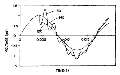
FIG. 1 is a diagrammatic representation of waveforms to illustrate various
conditions to
illustrate methods and arrangements of the present invention;
FIG. 2 is a flow diagram illustrating a specific implementation of the present
invention to
detect disturbances of a first type;
FIG. 3 is a flow diagram illustrating a specific implementation to detect
disturbances of a
second type;
FIGS. 4A and 4B provide a flow diagram illustrating a specific implementation
to
determine downstream faults in the context of the flow diagram of FIG. 2;
FIG. 5 is a one-line, block diagram representation of a system utilizing the
methods and
arrangements of the present invention;
FIG. 6 is a one-line, diagrammatic representation of portions of a solid-state
switch of
FIG. 5; and
FIG. 7 is a one-line, block diagram representation of another system with a
circuit
configuration different than that of FIG. 5.
-3-
CA 02617448 2008-02-07
DETAILED DESCRIPTION
Referring now to FIG. 1, in accordance with important features of the present
invention, a
method and arrangement are provided for detecting and responding to voltage
disturbances in an
electrical power system having alternating current sources. For example, a
waveform 120 of
FIG. 1 represents the voltage waveform of a fault condition and a waveform 130
represents the
voltage waveform where switching transients are present resulting from the
switching of a
capacitor bank. A waveform 140 represents the voltage waveform of a reference,
i.e. an ideal
waveform of an electrical power source where no voltage disturbances are
present. The method
and arrangement of the present invention detects the voltage disturbance
represented by the fault
waveform 120 while ignoring the transient response represented by the waveform
130.
Specifically, and with reference now to FIG. 2, the method and arrangement of
the
present invention initiates an integration when the actual source voltage
varies from the reference
by a predetermined tolerance or threshold amount, e.g. 5% in a specific
embodiment. In various
illustrative embodiments, the reference is obtained either as a predetermined
ideal waveform or a
sample derived from one or more preceding cycles of the actual source
waveform. The
integration then takes place over a predetermined integration time, e.g.
approximately 1/8 of a
cycle in a predetermined embodiment. If the resulting integration value at the
end of the
integration period exceeds a predetermined value, e.g. .6 millivolts. seconds
in a specific
embodiment, a predetermined disturbance condition is established. Depending on
the type of
disturbance condition that has been detected, e.g. a substantial sag
condition, appropriate action
is taken by associated circuit arrangements, e.g. perform a regulator
function, discontinue the
supply of power to the load, or transfer the load to an alternate source.
The flow diagram of FIG. 2 illustrates one basic implementation of the
detection of
voltage disturbances in accordance with the present invention. The flow
process begins with
initializing in a function block 50 and the obtaining of voltage sample data
in a process block 52.
The process flow continues to a process block 54 to compare the measured and
reference
waveforms, specifically, to calculate a parameter denoted "E 1 " obtained by
subtracting the actual
voltage sample from the reference voltage data. The process flow then
continues to a
-4-
CA 02617448 2008-02-07
determination block 56 to determine if the integration process is already in
process, i.e.
specifically if the integration counter is greater than zero. If the
integration process is already in
process, i.e. integration counter greater than zero, the process flow proceeds
to a process block 58
to increase the integration counter by one count and to calculate and store a
parameter denoted
"E2" which is obtained by multiplying E1 by the sign of the voltage of the
reference waveform.
Multiplication by the sign of the reference waveform is necessary to provide
appropriate
integration where the waveforms include transition through zero voltage and
preserves the
convention of the sense of the parameters being greater than or less than the
reference waveform,
i.e. a swell will always be negative and a sag will always be positive. If it
is determined in the
determination block 56 that the integration counter is not greater than zero,
i.e. the integration
process is not currently in process, the process flow proceeds to a
determination block 60 to
determine if the difference parameter E 1 between the actual and reference
waveforms is greater
than a tolerance or threshold, e.g. 5 percent in the specific example.
If the difference El does not exceed the specified value, the process flow
returns to the
process block 52. If the difference E1 exceeds the specified value, the
process flow proceeds to a
determination block 61 to determine if the present point on the waveform is in
an appropriate
range to begin an integration process. For example, in a specific embodiment,
if the point is
within approximately .5 milliseconds of a voltage zero, this is an
inappropriate point to begin
integration. This is done to prevent false initiation of the integration
process that might prevent
response to legitimate faults. If the point-on-wave is not within the
undesired range, the
determination in the determination block 61 is no and the process flow
proceeds to the process
block 58 as already discussed. If the determination in the determination block
61 is yes, i.e. that
the point-on-wave is in the undesired range, the process flow returns to the
process block 52.
From the process block 58, the process flow of FIG. 2 then proceeds to a
determination
block 62 to determine if the integration process of the specified number of
samples in a specified
time interval is complete, i.e. is integration count complete? If the
integration count is not
complete, the process flow returns to the process block 52 to continue the
integration process
until the specified number of integrations has been completed. If the
integration count is
complete, e.g. in a specific example 25 integration samples have been
completed, the process
-5-
CA 02617448 2008-02-07
flow proceeds to a process block 64 to reset the integration count, then to a
process block 66 to
integrate the set of error voltages, e.g. according to a trapezoidal rule in a
specific example.
For example, the following equation is utilized in one particular illustrative
implementation to provide the integral denoted "I" as follows:
Vo + VN N- I
2
I = 1=I
where Vo is the first sample and VN is the last sample in the integration set,
and At is the sample
interval. At this point, the results of the integration process are evaluated
and compared to
various specified values to determine what various disturbances have been
detected. For
example, in the specific example of the process flow of FIG. 2, the process
flow proceeds to a
process block 68 to look up a sag level 5 and a swell level 2 threshold. In a
preferred
embodiment, the threshold is varied based on the point on wave where the
disturbance is
detected.
The process flow then proceeds to a determination block 70 where the integral
I is
compared to the threshold level. If this sag level 5 threshold is exceeded, a
transfer flag is set at
72. If the sag threshold is not exceeded, the process flow proceeds to a
determination block 74 to
determine if the integral I is less than a swell level 2 threshold (negative
number), corresponding
to a substantial swell disturbance. If the swell threshold is established, a
transfer flag is set at 76.
If the swell threshold is not met, the process flow returns to the process
block 52 to continue the
process to detect voltage disturbances. For a multi-phase system, the flow
diagram of FIG. 2 is
implemented for each phase for which detection is desired such that a voltage
disturbance may be
detected and a decision to transfer requested for each of the phases on an
independent basis.
Thus, in accordance with the practice of the method of FIG. 2, the detection
of a voltage
disturbance and the request for transfer is completed within approximately 2
milliseconds or'/4 of
a cycle for a 60 hz system.
-6-
CA 02617448 2008-02-07
While the method and arrangement illustrated by the flow diagram of FIG. 2 may
be
utilized to detect various voltage disturbances, it is especially useful to
detect those disturbances
that are judged to be quite substantial such that so-called instantaneous
detection and response is
desirable, instantaneous in this context being most accurately defined as
without the introduction
of any intentional delay. Considering other less substantial or severe voltage
disturbances, the
detection and response process is not required to be so rapid especially since
it is typical to wait
various predetermined or user adjustable delay times before responding and
taking action after
such less severe disturbances are detected. For example the following is an
illustrative example
of how various disturbances may be categorized according to their severity or
substantiality of
departure from the nominal supply waveform along with illustrative selected
response times,
which as discussed may be varied and user selected along with the levels of
the % values from
nominal for the various categories:
Category % from nominal % of nominal response in cycles
sag level l -5% 95% 10
sag level 2 -10% 90% 7
sag level 3 -15% 85% 4
sag level 4 -20% 80% 1
sag level 5 -30% 70% instantaneous
swell level 1 +10% 110% 7
swell level 2 +20% 120% instantaneous
In accordance with important aspects of the present invention and with
additional
reference now to FIG. 3, while the disturbance detection method described
hereinbefore that
utilizes integration is desirable for the category disturbances of sag level 5
and swell level 2,
various of the remaining categories are detected utilizing a method and
arrangement based on
changes in the rms voltage or "rms-type" time-averaged voltage characteristics
rather than the
volts seconds product of the difference between the actual and reference
voltages. Considering
-7-
CA 02617448 2008-02-07
an illustrative example of this method and arrangement depicted in the flow
diagram of FIG. 3,
the process flow begins with initializing in a block 80 and the obtaining of
rms voltage sample
data in a process block 82. In various implementations, this data is derived
from a portion or one
or more current or previous cycles of the source waveform. The process flow
continues to a
process block 84 where the data values are updated and stored and then to a
detector section
generally referred to at 85. In a preferred embodiment, the detector 85 is
representative of a
plurality of such detectors, one for each of the disturbance categories to be
detected in addition to
the instantaneous categories, e.g. 5 in the categorization above (sag levels 1-
4 and swell level 1).
The detector section 85 includes a determination block 86 which determines if
the sample
rms voltage is lower (greater for swells) than a predetermined level denoted
"X" that is as
specified for each of the disturbance categories of interest in accordance
with the foregoing table.
Functionally, the determination is whether or not the sample data compared to
the predetermined
level X exceeds the deviation of the level X from nominal. If the rms voltage
sample does not
exceed the deviation, i.e. is not lower (greater for swells), the process flow
proceeds to a process
block 88 in which the detector buffer is decremented, e.g. a subtraction of
one count, and the
process flow returns to the process block 82. If the rms sample voltage is
below the specified
level (above for swells), the process flow proceeds to a process block 90
wherein the detector
buffer is incremented by adding one. The process flow then proceeds to a
determination block
92 to determine if the total in the detector buffer exceeds the specified
predetermined value
which may also be characterized as a threshold level. If the threshold is
exceeded, the process
flow proceeds to set a flag indicating a disturbance detection requiring a
transfer, e.g. as
input/output data to associated process and control apparatus. If the
threshold is not exceeded in
the determination block 92, the process flow returns to the process block 82.
Accordingly, the
method of FIG. 3 provides a net summing or time averaging of the comparison
over time
between the actual voltage samples and the predetermined levels representing
various sag/swell
deviations from nominal. For swell level determinations, the sample and the
level X may be
considered as negative numbers such that a swell greater than the level X is
considered lower or
exceeding the level X in the determination block 86.
-8-
CA 02617448 2011-03-09
In a multi-phase system, the process of FIG. 3 is implemented for each phase
for which
independent detection is desired, i.e. such that a disturbance detection
process is simultaneously
provided for each of the phases. It should also be understood that in various
embodiments, the
process of the flow diagram of FIG. 3 may be implemented for one or more of
various
disturbance categories with selected predetermined detection levels and
response times related to
the predetermined values or thresholds. It should also be realized that the
response time in cycles
and the specified threshold levels (also characterized as predetermined
values) are related but
may be different based on the frequency of the sample data and process cycle
of the detector 85,
e.g. less than, equal to, or greater than once per cycle of the source
waveform, etc.
Considering other important aspects of the present invention, a method and
arrangement
are provided to determine whether or not a detected fault condition is
upstream or downstream of
the observation or detection point in the power system, i.e. with respect to
the source connection
supplying the downstream load. When conditions are detected corresponding to
faults, e.g. a sag
level 5, while it is, of course, desirable to discontinue the supply of a load
from a source that has
an upstream fault, it would be undesirable to transfer the supply of the load
to another source
where the fault is downstream of the source connections.
With additional reference now to FIGS. 4A and 4B, an illustrative flow diagram
depicts an
illustrative specific embodiment to determine downstream faults in the context
of the disturbance
detection method and arrangement of FIG. 2 for the instantaneous response
categories. In the
illustrative example characterized as an overcurrent inhibit or OCI process,
the process flow
begins with initializing in a block 150 and the obtaining of voltage and
current sample data in a
process block 152, the data samples being denoted Vact and Iload. The process
flow then
proceeds generally along the lines as in the flow diagram of FIG. 2 utilizing
flow blocks 154,
156, 158, 160, 161, 162, 164, 166, 168, 170, 172, 174 and 176 functioning as
the corresponding
flow blocks 54, 56, 58, 60, 61, 64, 66, 68, 70, 72, 74 and 76 respectively.
In the process flow of FIG. 4A between the flow blocks 154 and 156, a process
block 155
is provided to establish a current threshold current parameter INmin, obtained
as the minimum of
n samples of the current Iload. The threshold is thus obtained to avoid
contribution by spurious
measurements. As shown in FIG. 4B, a determination block 180 utilizes the
parameter INmin to
determine if the
-9-
CA 02617448 2008-02-07
sampled current exceeds a threshold indicating a downstream fault, i.e. a
current which is larger
than load outrush conditions and upstream faults. This determination is made
when it has been
determined in the determination block 162 that the integration count is not
complete, i.e. during
each loop of the integration process. If it is determined in the block 180
that the current sample
indicates a downstream fault, an overcurrent inhibit state or flag is set in
block 182, denoted
"OCI", the consequences of which will be explained in more detail hereinafter.
In the process flow between the blocks 168 and 170, a determination block 184
is
provided to determine if the OCI flag is set at 182. If the OCI flag is set,
the process flow
proceeds to an inhibit transfer termination block 186 as an output indicating
that any transfer
response (i.e. transferring the load from the existing source to another
source) should be inhibited
due to the presence of a downstream fault. Considering additional aspects of
the OCI process,
between the flow blocks 170 and 176, a determination block 188 is provided to
determine if the
point on the waveform, denoted "POW", is between 120-165 degrees or 200-245
degrees. If it is
determined that the waveform is being sampled in that range during the
integration process, the
program flow proceeds to a process block 190 to set a delay transfer flag and
initiate a 1/8 of a
cycle count to provide a delay function before the process flow proceeds to
the determination
block 180 to determine if the current threshold establishes a downstream
fault. The delay
provided via the process block 190 is necessary for this range of points on
the waveform since a
fault occurring at minor sub loops at the end of each half cycle can interfere
with the obtaining of
accurate current data samples, the delay allowing time for the current to
build to levels for proper
detection. The "POW" parameter is obtained in a process block 192 located in
the process flow
between the flow blocks 160 and 158.
Considering additional features of the OCI method and arrangement, when the
determination in the block 180 establishes that the sampled current does not
indicate a
downstream fault condition, the process flow proceeds to a determination block
194 to determine
if a transfer delay flag has been set, in block 190. If no transfer flag has
been set, the process
flow returns to the process block 152. If the transfer flag has been set, the
process flow proceeds
to a process block 196 that increments a timer and then to a determination
block 198 to
determine whether or not the 1/8 of a cycle delay has elapsed. If the delay
has elapsed, the
-10-
CA 02617448 2011-03-09
process flow proceeds to a determination block 200 to determine if the OCI
flag is set. If the
OCI flag is not set, the process flow proceeds to the transfer block 176. If
the OCI flag is set, the
process flow proceeds to an inhibit transfer termination block 202 to provide
output data
indicative that transfer to another source should be inhibited due to the
detection of a
downstream fault. The OCI flag, once set, is not reset until the fault
condition ceases.
Accordingly, the process of FIGS. 4A and 4B is useful to determine whether a
fault condition is
upstream or downstream and is especially useful along with the method of FIG
2. to detect
disturbances but to inhibit transfer when a disturbance is detected but
transfer is undesirable due
to the likely presence of a downstream fault condition. For example, the
process depicted in the
flow diagram of FIGS. 4A and 4B implements a control arrangement in accordance
with the present
invention to determine fault location as part of the implementation of the
voltage disturbance
arrangement of FIG. 2.
In accordance with other aspects of the present invention, other methods to
detect
downstream faults before transfer may also be utilized with the disturbance
detection method and
arrangement of FIG. 2 for the instantaneous response categories. For example,
three additional
methods are described herein, although it is thought that the aforementioned
OCI method of
FIGS. 4A and 4B is generally more accurate and reliable.
For example, in accordance with a first additional method to determine
downstream
faults before transfer, the interrelation of supply voltage and fault current
may be utilized. That
is, the direction of the fault current and normal system voltage can be
accurately compared to
determine whether the fault is upstream or downstream. When a fault occurs
downstream of a
measurement device, current must flow in a positive direction with respect to
the normal system
voltage. For a sinusoidal voltage and fault switching angles in the range 0-
it radians (positive
half cycle), the fault current will, initially move in an increasingly
positive direction, and for
switching angles in the range it to 2n radians (negative half cycle), the
fault current will tend
towards an increasingly negative value initially. When the fault is upstream
of the measurement
device, the opposite is the case. Therefore, this can be utilized as a method
of determining the
direction of a fault. The reference voltage signal described hereinbefore can
be used to
accurately compare the fault current and the normal system voltage. For
relatively minor
-11-
CA 02617448 2008-02-07
upstream faults, there may be no significant change in the current.
Consequently, a second check
is required to verify whether the current is representative of a fault or of a
load. Fault currents
will achieve high absolute values with high rates of change. Since this
combination is unlikely to
occur for a normal system current, it is possible to set a combination of
threshold di/dt and an
absolute current value that are above levels presented by normal load
currents. To successfully
detect relatively low faults, a method can be utilized involving the
combination of a threshold
di/dt being exceeded and an absolute current magnitude being satisfied. While
this approach is
generally accurate in many situations, for portions of the source waveform
which may contain
minor sub-loops of current, i.e. those that occur close to the end of a half
cycle, this directional
detection method requires changes in the threshold values for detection. Thus,
the detection
method changes the threshold values in the vicinity of a voltage zero. This
entails choosing
detection of either phase to ground or phase to phase faults due to the
differences between these
fault types. The method must also accommodate the fact that minor sub-loops
associated with
phase-to-phase faults and phase-to-ground faults occur at different points in
the half cycle.
A second additional approach extends the method of the first additional
approach via the
interrelation of supply voltage and fault current via utilizing three phase-to-
ground and three
phase-to-phase current detectors that determine the direction and relative
magnitude of the
currents. The decision on whether or not a downstream fault exists is then
based on a polling of
the various detections. While this approach is believed to be generally
accurate for the various
downstream load connection arrangements, e.g. a secondary fault on a delta-wye
transformer,
there are a large number of variables and detectors and the majority decision
is determined by a
plurality of only one detector out of six as shown by the examples below,
where "U" denotes
upstream, "D" denotes downstream, and "X" denotes no determination:
-12-
CA 02617448 2008-02-07
EXAMPLE 1. C-phase fault to ground
Secondary side fault Primary side fault
t (ms) A AB B BC C CA poll A A B BC C C poll
B A
6 D D X U U D D X X X D U D D
8 D D X D D D D X X X U D D D
D D X D D D D X X X D D D D
12 D U X D D D D X X X D D D D
14 D D X U U D D X X X D D X D
EXAMPLE 2. Fault between phases B and C only
Secondary side fault Primary side fault
t (ms) A AB B BC C CA poll A A B BC C C poll
B A
6 U X D D D U D D X D D D U D
8 D X U U D D D D X U U D D D
10 D X D D D D D U X D D D D D
12 D X D D D D D D X D D D D D
14 U X D D D JU D D X D D D U D
5
A third additional approach is based on the conservation of the total system
energy when
a fault occurs. When a downstream fault occurs, the voltage sags toward zero
and a large current
flows. However, the total system energy does not change, but is merely
converted from one
form to another, the total magnetic flux in the system remaining virtually
constant during a fault.
10 If the fault is upstream, the point of reference is outside the conserved
flux system and the energy
will not appear to have been conserved. On the other hand, if the fault is
downstream, there
should be no observed change in the overall energy of the system. Further,
this method provides
-13-
CA 02617448 2011-03-09
implicit directionality since large flux deficits can only be accrued by
upstream faults, regardless
of whether the fault is phase to phase or phase to ground. The missing flux to
detect an upstream
fault is obtained by integrating the following difference equation with
respect to time:
AV = Vref -(V + Ldi/dt).
The inductance L of the system is relatively accurately determined and
typically in a relatively
narrow range. The missing flux can be measured against a reference flux that
accommodates
variations of the point on wave.
While the three additional approaches discussed hereinabove to detect
downstream faults
before transfer are relatively simple and generally useful, it is thought that
the aforementioned
OCI method of FIGS. 4A and 4B is generally more accurate and reliable, and
thus preferred.
In accordance with important aspects of the present invention, one particular
application
of the methods and arrangements to detect various disturbances is to respond
to disturbances in
an appropriate manner, e.g. by transferring the supply of a load from a first
source on which a
voltage disturbance is detected to a second source. Specifically and with
additional reference
now to FIG. 5, the flow diagrams of FIGS. 2, 3 and/or FIGS. 4A and 4B are
utilized to control the illustrative
source transfer switching system 10, which may be characterized as a power-
electronic switching
system, high-speed source-transfer switching system or HSSTSS. The high-speed
source-
transfer switching system (HSSTSS) 10 includes a controller stage 12 that
includes the process
implemented by the various flow diagrams of FIGS. 2-4AB. The HSSTSS 10
supplies a load at 14
with an alternating-current waveform via either a first AC source at 16 or a
second AC source at
18. The first and second AC sources 16 and 18 and the load at 14, as provided
in an electrical
power distribution system, are typically multi-phase circuits which are
represented in FIG. 5 by a
one-line diagram.
The HSSTSS 10 includes a first solid-state switch, SSS1, 20 and a second solid-
state
switch, SSS2, 22, the solid-state switches 20 and 22 also being referred to as
power electronic
switches. The HSSTSS 10 via the controller stage 12 controls either SSS1 to
supply the load at
14 via the first source 16 or controls SSS2 to supply the load at 14 via the
second source 18. The
samples of the voltage waveforms of each source 16, 18 are provided via
respective sensing
inputs at 24, 26. The controller stage 12 under the control of the various
flow diagrams of FIGS.
-14-
CA 02617448 2008-02-07
2-4 provides appropriate control signals at 28, 30 to control the operation of
each respective
solid-state switch, SSS1 20 and SSS2 22. For example, assume that SSS1 20 is
turned on by the
controller stage 12 via signals at 28 so as to be conductive and supply the
load at 14. If the
controller stage 12 via the sensing input 24 senses that the voltage of the
first source at 16 is
exhibiting undesirable characteristics, i.e. a substantial voltage disturbance
is detected, the
controller stage 12 via the control signals at 28, 30 turns off SSS1 and turns
on SSS2 so as to
transfer the supply of the load at 14 from the first source at 16 to the
second source at 18. As
used herein, the term "incoming" is used to describe the source and the SSS
that will be turned
on to supply the load (e.g. the second source at 18 and SSS2 in the
illustrative example), and the
term "outgoing" is used to describe the source and the SSS that is being
turned off (e.g. the first
source at 16 and SSS1 in the illustrative example).
Referring now to FIG.6, in a specific illustration, each of the solid-state
switches SSS 1
and SSS2 includes one or more arrays of back-to-back (inverse parallel)
connected thyristors,
e.g. 40a and 40b for SSS1 and 42a and 42b for SSS2. In illustrative
implementations, each array
of thyristors is rated in the range of 2-10kv. To provide operation in medium
voltage systems,
e.g. operating in the range of 2-34.5 kv, one or more of such thyristors SSS1
and SSS2 are
connected in series for each phase of the sources, e.g. a plurality of such
thyristors being referred
to as a stack. Thus, while the term thyristor is used for the solid-state
switches SSS1, 40 and
SSS2, 42, this commonly refers to a thyristor stack.
Considering now operation of the control arrangement and method of the
illustrative
HSSTSS 10, transfer of the load at 14 from one source to the other, e.g. the
first source at 16 to
the second source at 18, is generally accomplished by removing the gating
signals at 28a, 28b to
shut off SSS1 and starting the gating signals at 30a, 30b to turn on SSS2.
Thus, the first source
at 16 ceases to supply the load at 14 and the second source at 18 begins to
supply the load at 14.
The controller 12 performs the transfer and the application of the appropriate
gating signals to
avoid undesirable effects such as paralleling of sources and shoot-throughs.
Reference may be
made to U.S. Patent No. 5,808,378 issued on September 15, 1998 in the name of
R. P. O'Leary
and to copending Canadian application Serial No. 2,280,385 filed August 16,
1999 and issued
May 22, 2007.
-15-
CA 02617448 2011-03-09
Referring now additionally to FIG. 7 and considering another illustrative
source transfer
switching system 110 where more than two solid-state switches are controlled,
a controller 112
of a high-speed source-transfer switching system (HSSTSS) 110 controls solid-
state switches
SSS1, 123, SSS2, 122 and SSS3 121 via respective control signal paths 128,
131, and 132. The
specific illustrative circuit configuration of FIG. 7 implements a split-bus
primary selective
system, which is used to split the load during normal operation. Specifically,
in normal
operation, a first source 16 supplies a first load circuit 114 via SSS 1 and a
second source 18
supplies a second load circuit 116 via SSS2, with SSS3 normally being turned
off
(nonconducting) and functioning as a bus-tie switch. Thus, each of the sources
16, 18 is a
preferred source for its respective load circuit 114, 116 and each is an
alternate source for the
other load circuit, 116, 114 respectively. When one of the sources at 16, 18
is lost or exhibits
undesirable characteristics, the controller 112, after a transfer decision is
made, and as described
hereinbefore, removes the signals at 128 or 131 and applies signals at 132
such that the load
circuits 114, 116 are supplied from one of the sources at 16 or 18. For
example, if the source 16
is lost, SSS1, 123will be turned off and SSS3, 121, the bus-tie switch, will
be turned on to supply
the load circuit 114 while SSS2, 122 continues to supply the load circuit 116.
The polarity
comparison to establish the appropriate application of control signals in the
circuit configuration
of FIG. 7 utilizes the differential voltage across the incoming switch, e.g.
SSS3, 121 when
transferring the load circuit 114 so as to be supplied from the source 18 via
SSS3, 121 and SSS2,
122. Similarly, upon the return of the source 16, when the normal
configuration is to be restored,
the differential voltage across the incoming switch, e.g. SSS1, 123 is
utilized for the polarity
comparison.
When disturbances are detected via the methods of FIGS. 2 3 and/or 4A and 4B,
before any
transfer decision is made by the controllers 12 or 112 to discontinue the
supply of a load from a
first source and to supply that load from a second source, it is first
determined whether or not the
transfer will be to a source of better quality than the source currently
supplying the load. The
best source/load configuration is determined based on the measured values and
expected load
conditions, i.e. the source that is anticipated to serve the load(s) with
voltages within the nominal
range or of closest proximity thereto.
-16-
CA 02617448 2008-02-07
While there have been illustrated and described various embodiments of the
present
invention, it will be apparent that various changes and modifications will
occur to those skilled in
the art. Accordingly, it is intended in the appended claims to cover all such
changes and
modifications that fall within the true spirit and scope of the present
invention.
-17-