Note: Descriptions are shown in the official language in which they were submitted.
CA 02618688 2008-01-16
TOROIDAL INDUCTOR DESIGN FOR IMPROVED Q
The inventive arrangements relate generally to inductors and more
particularly to toroidal inductors.
Embedded toroidal inductors are known in the art. For example, U.S.
Patent No. http://patft 1.uspto. gov/netacgi/nph-
Parser? Sect 1=PTO 1 &Sect2=HITOFF&d=PALL&p=1 &u=%2Fnetahtml%2FPTO%2
Fsrchnum. htm&r=1 &f=G&1=5 0&s 1=6990729. PN. &OS=PN/6990729&RS=PN/6990
729 - hO#hOhttp://I)atftl.uspto.gov/netacgi/nph-
Parser?Sect1=PTO1 &Sect2=HITOFF&d=PALL&p=1 &u=%2Fnetahtml%2FPTO%2
Fsrchnum.htm&r=1 &f=G&1=50&s 1=6990729.PN.&OS=PN/6990729&RS=PN/6990
729 - h2#h26,990,729 to Pleskach et al. discloses a method for forming an
embedded
toroidal inductor. The method includes the step of forming in a ceramic
substrate a
first plurality of conductive vias radially spaced a first distance from a
central axis so
as to define an inner circumference. A second plurality of conductive vias is
formed
radially spaced a second distance about the central axis so as to define an
outer
circumference. A first plurality of conductive traces forming an electrical
connection
between substantially adjacent ones of the first and second plurality of
conductive
vias is formed on a first surface of the ceramic substrate. Further, a second
plurality
of conductive traces forming an electrical connection between
circumferentially offset
ones of the first and second plurality of conductive vias is formed on a
second surface
of the ceramic substrate opposed from the first surface to define a three
dimensional
toroidal coil.
In conventional embedded inductor designs of the prior art, there are
two components that comprise the toroidal inductor coil: conductive traces and
conductive vias. Of these two components, the conductive traces account for
the vast
majority of the direct current resistance (DCR) due to their very small cross
sectional
area in comparison to the conductive vias. DCR is defined as the resistance of
the
inductor winding as measured using direct current. Notably, an increase in the
value
of DCR will cause a decrease in the quality factor (Q) of the inductor.
-1-
CA 02618688 2008-01-16
Since Q is a measure of the relative losses in an inductor, the higher
the DCR, the lower the Q in the system. In many applications, it is desirable
to
provide an inductor with very high Q. Therefore, what is needed is an improved
toroidal inductor design that can reduce the direct current resistance of the
inductor
and thereby increase Q. At the same time, the design should not increase the x-
y
plane size of the toroidal footprint or require any additional machining or
post
processing steps.
The invention concerns an inductor and method for forming an
inductor. The inductor comprises a coil formed from an elongated conductor
extending around a core material and defining a plurality of turns. The
elongated
conductor includes one or more coil segments of a first type. Each coil
segment of
the first type is comprised of a plurality of elongated parallel conductors
spaced apart
and electrically connected by conductive links at predetermined intervals
along their
respective lengths. Each of the elongated parallel conductors is comprised of
a
conductive trace disposed on a surface of a substrate. Moreover, the
conductive links
are formed from vias defined in a substrate.
Further, the inductor is comprised of one or more coil segments of a
second type. Each coil segment of the second type is formed of a single
conductor.
In particular, the single conductor comprising the coil segment of the second
type
comprises a conductive via formed in a substrate. The coil segment of the
first type
and the coil segment of the second type are arranged in a series configuration
to form
the elongated conductor.
According to one aspect of the invention, the elongated conductor is
comprised of a plurality of coil segments of the first type and a plurality of
coil
segments of the second type. Each coil segment of the second type defines a
series
electrical connection between coil segments of the first type.
According to yet another aspect of the invention, the inductor can
include a coil formed from an elongated conductor extending around a core
material
and defining a plurality of turns. The elongated conductor includes a
plurality of coil
segments arranged in an alternating pattern of a first type segment and a
second type
-2-
CA 02618688 2008-01-16
segment. The first type segment comprises a plurality of parallel conductors
spaced
apart and electrically connected at predetermined intervals along a length of
the
plurality of parallel conductors. The second type segment comprises a single
elongated conductor comprised of conductive vias formed in a substrate. In
addition,
the conductive traces are connected at the predetermined intervals by one or
more
conductive vias.
The invention can also comprise a method for forming an inductor.
The method includes forming a coil from an elongated conductor extending
around a
core material to define a plurality of turns. The method also includes the
step of
forming the elongated conductor to include at least one coil segment of a
first type
comprised of a plurality of elongated parallel conductors spaced apart. The
elongated
parallel conductors are electrically connected by means of conductive links
spaced at
predetermined intervals along a length of the plurality of elongated parallel
conductors. Moreover, each of the parallel conductors is formed as a
conductive trace
disposed on a surface of the substrate. The conductive links are formed from
vias
defined in a substrate.
The method can also include the step of forming the elongated
conductor of at least one coil segment of a second type. The coil segment of
the
second type is formed of a single conductor. Each coil segment of the second
type is
formed as a conductive via formed in a substrate. Furthermore, one or more
coil
segments of the first type and one or more coil segments of the second type
are
arranged in a series configuration to form the elongated conductor. According
to one
aspect, the method includes the step of forming with at least one coil segment
of the
second type a series electrical connection between a plurality of the coil
segments of
the first type.
According to yet another aspect of the invention, the method can
include forming an elongated conductor which extends a plurality of turns
around a
core material to define a coil. The elongated conductor is selected to include
a
plurality of coil segments arranged in an alternating pattern of a first type
segment and
a second type segment. The first type segment is selected to include a
plurality of
-3-
CA 02618688 2008-01-16
parallel conductors spaced apart and electrically connected to each other at
predetermined intervals along a length of the plurality of parallel
conductors. The
second type segment includes a single conductor. The method further comprises
forming the second type segments as conductive vias disposed within a
substrate.
Moreover, each parallel conductor is formed as a conductive trace disposed on
a
surface of a substrate. The conductive traces are connected at the
predetermined
intervals by one or more conductive vias.
FIG. 1 is a schematic representation that is useful for understanding the
structure of an improved toroidal inductor.
FIGS. 2A and 2B illustrate a flow chart that is useful for understanding
the method of making the present invention.
FIG. 3 is a top view of a ceramic substrate layer with vias formed
therein that is useful for understanding the invention.
FIG. 4 is a cross-sectional view of the ceramic substrate layer of FIG.
3, taken along line 4-4.
FIG. 5 is a top view of the ceramic substrate layer in FIG. 3 after the
application of a pattern of conductive traces.
FIG. 6 is a cross-sectional view of the ceramic substrate layer of FIG.
5, taken along line 6-6.
FIG. 7 is a top view of a second ceramic substrate layer that is useful
for understanding the invention.
FIG. 8A is a cross-sectional view of the second ceramic substrate layer
of FIG. 7, taken along the line 8A-8A.
FIG. 8B is a partial expanded cross-sectional view of the second
ceramic substrate layer of FIG. 7, taken along the line 8B-8B.
FIG. 9 is a cross-sectional view showing the first ceramic substrate
layer being positioned on top of the second ceramic substrate layer.
FIG. 10 is a cross-sectional view of the first and second ceramic
substrate layers in a stacked configuration that is useful for understanding
the
invention.
-4-
CA 02618688 2008-01-16
FIG. 11 is a top view of a third ceramic substrate layer that is useful for
understanding the invention.
FIG. 12 is a cross-sectional view of the third ceramic substrate layer of
FIG. 11, taken along the line 12-12.
FIG. 13 is a cross-sectional view showing the third ceramic substrate
layer being positioned on top of the first and second ceramic substrate
layers.
FIG. 14 is a cross-sectional view of the first, second and third ceramic
substrate layers in a stacked configuration that is useful for understanding
the
invention.
FIG. 15 is a top view of a fourth ceramic substrate layer that is useful
for understanding the invention.
FIG. 16 is a cross-sectional view of the fourth ceramic substrate layer
of FIG. 15, taken along the line 16-16.
FIG. 17 is a cross-sectional view showing the fourth substrate layer
being positioned underneath the first, second, and third ceramic substrate
layers.
FIG. 18 is a cross-sectional view of the first, second, third, and fourth
ceramic substrate layers in a stacked configuration that is useful for
understanding the
invention.
FIG. 19 is a cross-sectional view of a second alternative embodiment
of the toroidal inductor shown in FIG. 18.
The invention concerns an improved toroidal inductor integrated
within a ceramic substrate and a method of making same. For convenience, the
substrate is described herein as a ceramic substrate. However, it should be
understood
that the invention is not limited in this regard. Substrates formed of other
materials
can also be used. For example, such materials include, but are not limited to
liquid
crystal polymer (LCP), polymer film, polyimide film, epoxy laminates, or
semiconductor materials such as silicon, gallium arsenide, gallium nitride,
germanium
or indium phosphide.
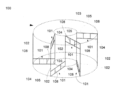
Referring to FIG. 1, a schematic representation of the improved
toroidal inductor 100 is shown. The inductor 100 comprises a coil formed of an
-5-
CA 02618688 2008-01-16
elongated conductor defining a plurality of turns and extending around a core
material
103. The improved toroidal coil structure includes a plurality of coil
segments
arranged in an alternating pattern. The coil segments include a first type
coil segment
101 and a second type coil segment 102. The first type coil segment 101 is
comprised
of a plurality of elongated parallel conductors 104, 105. A first elongated
parallel
conductor 104 forms a first parallel conductor pair with a second elongated
parallel
conductor 105. The parallel conductors 104, 105 are spaced apart from each
other
and electrically connected at locations along their elongated length by at
least one first
conductive link 108. The second type coil segments 102 provide a series
electrical
connection between spaced apart ones of the first type coil segment 101.
In a conventional embedded toroidal inductor, a first type coil segment
101 is formed of a single conductive trace disposed on a surface of a
substrate.
However, such conductive traces have a relatively low cross sectional area.
Accordingly, they tend to have a relatively high resistance. In the present
invention,
this problem is overcome by using a plurality of elongated parallel conductors
104,
105 to decrease the direct current resistance. Conventional embedded toroidal
inductors do not make use of separate parallel conductors to form a first type
coil
segment 101. In the present invention, conductive links 108 are used to
minimize the
effect of any capacitance that might otherwise exist as between the elongated
parallel
conductors 104, 105. The second type coil segments 102 can be formed as
conductor
filled vias using conventional circuit board manufacturing techniques.
A method for manufacturing a toroidal inductor having the form shown
in FIG. 1 shall now be described in the flowchart in FIGS. 2A and 2B and with
reference to FIGS. 1 and 3-19. Referring now to FIGS. 3 and 4, the method can
begin
with step 202 by forming a suitably sized piece of an unfired ceramic
substrate layer
300. The ceramic substrate layer 300 can be any of a variety of commercially
available glass ceramic substrates designed to be calcined at 800 C to 1,050
C. This
class of materials is commonly referred to as low-temperature co-fired
ceramics
(LTCC). Such LTCC materials have a number of advantages that make them
especially useful as substrates for RF systems. For example, low temperature
951 co-
-6-
CA 02618688 2008-01-16
fire Green TapeTM from Dupont is Au and Ag compatible, and it has a thermal
coefficient of expansion (TCE) and relative strength that are suitable for
many
applications. Other similar types of ceramic tapes can also be used. The size
of the
ceramic tape can be determined by a variety of factors depending upon the
particular
application. For example, if the toroidal inductor is to form part of a larger
RF circuit,
the ceramic tape can be sized to accommodate the RF circuit in which the
toroidal
inductor forms a component.
A first plurality of conductive vias 302 and a via 312 can be formed in
the unfired ceramic substrate layer 300. This step can be performed using
conventional techniques. For example, vias can be formed by punching, laser
cutting,
or etching holes in the unfired ceramic substrate layer 300. As shown in FIGS.
3 and
4, the first plurality of conductive vias 302 can be radially spaced a first
distance dl
from a central axis 401 so as to define an inner circumference of a toroidal
inductor.
In step 206, a second plurality of conductive vias 304 can be similarly formed
radially
spaced a second distance d2 about the central axis 401 so as to define an
outer
circumference. As shown in FIG. 4, the vias can extend substantially between
opposing surfaces 306, 408 of the ceramic substrate layer 300. Each conductive
via
302 can be positioned radially adjacent to a conductive via 304.
In general, the term "radially adjacent" means that two vias that are
approximately radially aligned relative to central axis 401 and positioned
adjacent to
each other. Vias 302A and 304A are examples of radially adjacent vias.
However, it
should be noted that radially adjacent conductive vias, as that term is used
herein, are
not necessarily precisely aligned radially. Such radially adjacent vias can
also include
vias that are offset circumferentially from one another to some degree. In
contrast,
vias 302A and 304B represent circumferentially offset vias. As can be seen in
FIG. 3,
circumferentially offset vias are not aligned radially. In step 208, the via
holes of the
first and second pluralities of conductive vias 302, 304 are filled with
conductive
paste or any other suitable conductive element.
Referring now to FIGS. 5 and 6, the process can continue in step 210
by disposing a first plurality of conductive traces 510 on ceramic substrate
layer 300.
-7-
CA 02618688 2008-01-16
The first plurality of conductive traces 510 on surface 306 form electrical
connections
between respective ones of the first plurality of conductive vias and second
plurality
of conductive vias that are substantially radially adjacent, as defined
earlier.
Moreover, additional conductive traces 514 and 516 can also be added to
facilitate in
the formation of electrical terminals. The conductive traces 510 can be formed
using
conventional PCB methods which are known to the skilled artisan, such as thick
film
screen printing, photoengraving, and PCB milling.
Referring now to FIGS. 7, 8A, and 8B, the process continues by
forming a second ceramic substrate layer 700. In step 212, a third plurality
of
conductive vias 803 are formed at predetermined intervals through the second
ceramic
substrate layer 700. The third plurality of vias 803 is located within a
predetermined
area which corresponds to each of the respective lengths of second conductive
traces
710 (discussed below). This concept is best understood by referring to FIG.
8B. As
shown in FIG. 8B, each trace 710 has the third plurality of vias 803
positioned at
locations along the length of the trace 710 and at opposing ends of the trace
710. In
step 214, the third plurality of conductive vias 803 are filled with
conductive paste or
any other suitable conductive element. In step 216, a second plurality of
conductive
traces 710 is provided on surface 706 of the second substrate layer 700.
Moreover,
additional conductive trace 717 can also be added to facilitate in the
formation of
electrical terminals. The second plurality of conductive traces 710 is
arranged so that
when the first and second ceramic substrate layers 300, 700 are aligned and
stacked as
shown in FIGS. 9 and 10, the traces 710 on surface 706 will provide an
electrical
connection between circumferentially offset ones of the first and second
pluralities of
conductive vias 302, 304.
Referring now to FIGS. 11 and 12, the process continues by forming a
third ceramic substrate layer 1100. In step 218, a fourth plurality of
conductive vias
1203 are formed at predetermined intervals through the third ceramic substrate
layer
1100. The hole locations are defined within the respective lengths of third
conductive
traces 1110 (discussed below). In step 220, the fourth plurality of conductive
vias
1203 are filled with conductive paste or any other suitable conductive
element. In
-8-
CA 02618688 2008-01-16
step 222, the third plurality of conductive traces 1110 is provided on surface
1106 of
the third substrate layer 1100. Moreover, additional conductive traces 1114,
1116 can
also be added to facilitate in the formation of electrical terminals.
The third plurality of conductive traces 1110 is arranged so that when
the ceramic substrate layers 300 and 1100 are aligned and stacked as shown in
FIGS.
13 and 14, the traces 1110 on surface 1106 and the conductive traces 510 on
surface
306 define a plurality of elongated parallel conductors. The elongated
parallel
conductors are aligned with each other, spaced apart and electrically
connected by
conductive links defined by the fourth plurality of conductive vias 1203.
Referring now to FIGS. 15 and 16, the process continues by forming a
fourth ceramic substrate layer 1500. In step 224, a fourth plurality of
conductive
traces 1510 is provided on surface 1506 of the fourth substrate layer 1500.
The fourth
plurality of conductive traces 15 10 are arranged in the same manner as the
second
plurality of conductive traces 710. Moreover, additional conductive trace 1517
can
also be added to facilitate in the formation of electrical terminals.
The fourth plurality of conductive traces 1510 is arranged so that when
the ceramic substrate layers 700 and 1500 are aligned and stacked as shown in
FIGS.
17 and 18, the traces 710 on surface 706 and the conductive traces 1510 on
surface
1506 define a plurality of elongated parallel conductors. The elongated
parallel
conductors are aligned with each other, spaced apart, and electrically
connected by
conductive links defined by the fourth plurality of conductive vias 1203. The
combination of elongated parallel conductors and conductive links serves to
lower the
direct current resistance in the system by increasing the effective cross-
sectional area
of the traces, hence improving the quality factor (Q) of the inductor. For
example, in
testing using standard DCR measuring instruments, the improved toroidal
inductor
design had a lower DCR value as compared to conventional toroidal inductors.
Specifically, the DCR value was reduced by nearly one-half.
The conductive traces 510, 710, 1110, and 1510 can be formed of any
suitable conductive film, paste, or ink that is compatible with the co-firing
process for
the selected LTCC material. Such materials are commercially available from a
-9-
CA 02618688 2008-01-16
variety of sources. Further, it should be noted that for purposes of
consistency with
standard LTCC processing, each of the ceramic substrate layers shown in FIGS.
6,
8A, 12, and 16 contain conductive traces disposed on one side of each ceramic
substrate layer only. However, the invention is not so limited. Those skilled
in the art
will appreciate that it is possible for the conductive traces to instead be
disposed on
opposing sides of a single layer of ceramic tape. Such alternative
arrangements are
intended to be within the scope of the invention. For example, such an
alternative
arrangement is shown in FIG. 19, where structure common to FIG. 18 is
identified
using like reference numerals. FIG. 19 shows second ceramic substrate layer
700,
which includes conductive traces 710 and 1510 disposed on opposing sides. In
step
226, the various LTCC layers 300, 700, 1100, and 1500 can be stacked and
aligned
with one another, as well as laminated by utilizing conventional processing
techniques.
In their stacked configuration shown in FIG. 18, the conductive vias
302, 304, 803, 1203 and the conductive traces 510, 710, 1110, and 1510 in FIG.
18
together define a three dimensional conductive toroidal coil 100, which is
best
illustrated by the schematic representation in FIG. 1. In particular, FIG. 1
is useful for
understanding the toroidal coil structure of the inventive arrangements. In
this regard,
it should be understood that the invention herein is not limited to the
precise
arrangement or pattern of vias 302, 304, 803, 1203 and traces 510, 710, 1110,
1510
illustrated in FIG. 18. Instead, any pattern, geometry, and number of vias and
traces
formed in the ceramic substrate layer can be used provided that it generally
results in
a substantially toroidal coil arrangement of the kind similar to that
illustrated in
FIG. 1
In FIGS. 1 and 3-19 there is shown a toroidal coil in which the parallel
conductive traces are comprised of only two elongated parallel conductors 104,
105.
It should be understood, however, that the invention is not limited in this
regard.
Three or more parallel elongated conductors can also be used, with each
elongated
parallel conductor conductively linked with an adjacent layer by means of a
plurality
-10-
CA 02618688 2008-01-16
of conductive links disposed along the elongated length of each elongated
parallel
conductor.
Referring back to FIGS. 3, 5, 7, and 11, the combination of additional
conductive vias 312 and additional conductive traces 514, 516, 717, 1114,
1116, and
1517 can be provided to define a set of electrical contacts for the toroidal
inductor.
Once all of the vias and traces are completed, the ceramic substrate layers,
vias and
traces can be fired together in step 228 in accordance with a temperature and
time
appropriate for the particular type of ceramic tape to sinter and densify.
-11-