Note: Descriptions are shown in the official language in which they were submitted.
CA 02620053 2008-02-21
- 1 - 2004P15622 rws
Patent-Treuhand-Gesellschaft
fur elektrische Gluhlampen mbH., Munich
Electronic ballast for discharge lamps having an EOL monitoring
circuit
Technical field
The invention is based on AC operation of discharge lamps using
electronic ballasts.
Prior art
Discharge lamps of various designs are nowadays usually
operated using electronic ballasts. Such ballasts generally
contain high-frequency converters for generating an AC supply
power for the lamp from a low-frequency system supply or else
from a DC voltage supply.
In addition to the essential functions for starting and
operating the discharge lamp, electronic ballasts often also
have additional monitoring and regulation functions. In the
present context, so-called EOL monitoring (end of life
monitoring) is of interest, in which a circuit element of the
ballast is used to monitor when an end of life of one of the
electrodes of the discharge lamp operated is indicated.
Such EOL monitoring circuits are known per se, for example from
WO 00/11916, to which reference is made, by way of summary, for
explaining the technical background. In particular, this
document explains the fact that the rectifying properties of
the discharge lamp which are established as the end of life of
the electrode approaches are utilized for EOL monitoring. The
end of life of the electrode entails consumption or degradation
of an electron emitter material. In more general terms, the end
of life of an electrode is indicated by a rise in the electron
work function at this electrode. This results in asymmetry
CA 02620053 2008-02-21
- 2 - 2004P15622 rws
during AC operation or, in other words, a unipolar additional
power in the lamp having a corresponding asymmetrical voltage
drop.
Description of the invention
The object of the present invention is to specify an electronic
ballast for discharge lamps which is improved as regards EOL
monitoring.
The invention firstly relates to an electronic ballast for AC
operation of a discharge lamp having an EOL monitoring circuit
for detecting the end of life of the electrodes of the
discharge lamp, which EOL monitoring circuit responds to an
asymmetrical power of the discharge lamp, characterized in that
a current associated with the asymmetrical power and a
reference current are fed to a current differential amplifier
in the EOL monitoring circuit,
to a corresponding lamp system comprising such a ballast
together with an appropriate discharge lamp.
Preferred refinements are specified in the dependent claims and
will be explained in more detail below.
The basic concept of the invention consists in, as a deviation
from the prior art, not deriving a voltage correlating with the
beginning rectifying properties of the discharge lamp,
detecting it via a voltage-sensitive amplifier circuit and
using it for controlling the operation of the ballast, but
instead carrying out current differential amplification. For
this purpose, a current correlating with the asymmetrical power
of the discharge lamp is used and fed, together with a
reference current, to a current differential amplifier. The
current differential amplifier is characterized by the fact
that it permits input currents, even when an EOL is not
detected, i.e. no rectifying properties can yet be detected. It
CA 02620053 2008-02-21
- 3 - 2004P15622 rws
is therefore possible, in particular, to avoid a situation in
which voltage displacements result in the case of voltage-
sensitive inputs with transistors, which are connected in the
case of an EOL detection, as a result of the then occurring
current load on resistors, with which corresponding measured
voltages for detection purposes or reference voltages for
comparison purposes are generated.
In particular in WO 00/11916 mentioned above, two voltage
divider circuits subject one another to a load since a current
is formed from a voltage differential signal, which current
represents the further signal variable. This results in a
parasitic voltage displacement, a dependence on the absolute
values of the potentials used with respect to the reference
potential and nonlinear dependencies on the potential
differences.
In contrast to this, current inputs are used in the invention
which may also carry currents in the normal operating case,
with the result that no substantial displacements result in the
case of an EOL detection.
Owing to resistors in the power supply lines having a
correspondingly high resistance value, the measured current
required and the reference current can be reduced to such small
values that the associated power consumption is completely
insignificant. In addition, suitable working points can easily
be set owing to corresponding initial loads, for example owing
to feedback at the current differential amplifier.
One preferred refinement of the input of the current
differential amplifier consists in a current mirror circuit
known per se, the current differential amplifier moreover
particularly preferably being in the form of an operational
amplifier. Such OP amplifiers with a mirror input are
obtainable, for example, as so-called Norton amplifiers by
Motorola, nowadays "On Semiconductors".
CA 02620053 2008-02-21
- 4 - 2004P15622 rws
This Norton amplifier also has a voltage output and therefore
has a further preferred feature of the invention. Finally, the
amplifier is one which has a MOSFET current mirror input, a
favorable embodiment of such a current mirror input. Moreover,
current mirror inputs may, however, also be designed using
other unipolar technology or else using bipolar technology.
In one simple and favorable refinement of the invention, an
output signal from the current differential amplifier can be
passed on to a window comparator, i.e. a combination of two
simple comparators, whose threshold values provide a
corresponding window. The output signals of the comparators can
be linked, for example, via a NAND gate and fed to a shutdown
device, which takes the high-frequency converter out of
operation in the event of the end of life of an electrode being
detected.
Since parasitic oscillations and harmonics may result in the
ballast during operation, in particular transient responses are
possible at the beginning of operation, the EOL monitoring
circuit preferably has a low-pass filter, for example an RC
element. In one favorable refinement, the capacitor of the RC
element may be positioned between the measured current input of
the current differential amplifier and the ballast-internal
reference potential.
Instead of an evaluation using comparators and logic gates,
which is particularly suitable for discrete implementations,
microprocessor sampling of the current differential amplifier
may also be provided, which samples at specific time intervals
and possibly carries out repeat interrogations in the case of
an EOL detection for safety reasons. In this case, note should
be made of the fact that the response times prescribed by
standards and/or the technical boundary conditions for EOL
monitoring circuits are not particularly short, but a few
seconds time is generally available. Finally, it is generally
CA 02620053 2008-02-21
- 5 - 2004P15622 rws
only critical to avoid thermal damage and, for example,
resultant fire hazards owing to electrodes returning to the
asymmetrical additional power in the lamp. These thermal
processes are comparatively slow.
One possibility for generating a reference current for the
current differential amplifier consists in deriving a current
from a reference potential via a resistor having a relatively
high resistance value, in particular by the ballast-internal
high-frequency converter.
In many cases which are important in practical terms, a so-
called coupling capacitor is present between the discharge lamp
and the ballast-internal reference potential, which coupling
capacitor is generally charged to a mid-potential between the
ballast-internal supply potential and the reference potential
during operation and therefore ensures true AC operation of the
discharge lamp. With this circuitry, the current differential
amplifier, which moreover has a reference to this reference
potential, can favorably be connected to a tap between the
coupling capacitor and the discharge lamp via resistors in
order to therefore tap off a current correlating with the
voltage across the coupling capacitor. In this case, it is
necessary to take into account the fact that the inputs of the
current differential amplifier are very close to the reference
potential in terms of their potential.
Other circuitry which is important in practical terms provides
a corresponding coupling capacitor between the AC output of the
high-frequency converter and the discharge lamp and
correspondingly then generally connects the other terminal of
the discharge lamp directly to the reference potential. Owing
to the fact that resonant capacitors, which are required in
particular for resonant starting processes, are connected in
parallel with the lamp, such circuits may be particularly
advantageous for being able to measure the lamp current in a
simple and direct manner and to use it, for example, for
CA 02620053 2008-02-21
- 6 - 2004P15622 rws
current regulation purposes. In this case, it is favorable to
derive the measured current for the current differential
amplifier, which in turn has a reference to the reference
potential, in turn from a center tap between the coupling
capacitor and the discharge lamp via a resistor. This measured
current then correlates with the lamp voltage, i.e. would have
an average value of zero during true AC operation in a smoothed
manner. In this case, the corresponding measured current input
of the current differential amplifier may be subjected to an
initial load, for example, via feedback from the amplifier
output, for which purpose reference is also made to the second
exemplary embodiment.
One preferred application of the invention is in low-pressure
discharge lamps, but it is also suitable for high-pressure
discharge lamps.
In addition, the invention has a method aspect and
correspondingly also relates to a method for AC operation of a
discharge lamp using such a ballast, in which method the end of
life of an electrode of the discharge lamp is detected by an
EOL monitoring circuit, which responds to an asymmetrical power
of the discharge lamp, characterized in that a current
associated with the asymmetrical power and a reference current
are fed to a current differential amplifier in the EOL
monitoring circuit. The individual features explained above and
below are also implicitly critical to the method aspect of the
invention.
Brief description of the drawings
The invention will be explained in more detail below with
reference to exemplary embodiments, it being possible for the
individual features also to be essential to the invention in
other combinations, and these individual features relating both
to the apparatus aspect and to the method aspect of the
invention.
CA 02620053 2008-02-21
- 7 - 2004P15622 rws
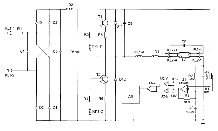
Figure 1 shows a simplified circuit diagram of a ballast for a
low-pressure discharge lamp as a first exemplary
embodiment.
Figure 2 corresponds to figure 1 and shows a second exemplary
embodiment.
Figure 3 corresponds to figure 1 and shows a third exemplary
embodiment.
Preferred embodiment of the invention
Figure 1 shows a circuit diagram of a ballast according to the
invention for a low-pressure discharge lamp LA1, which is
likewise illustrated in the right-hand region and is connected
in the left-hand region to the input terminals KL1-1 and KL1-2
for a customary domestic power supply by a phase line L and a
neutral line N. The inductor LD2 and the capacitor C5 form a
radio interference suppression filter between the rectifier D1
to D4 and an intermediate circuit storage capacitor C6, across
which the intermediate circuit voltage is present with a
ballast-internal reference potential, in the lower region of
the figure, and a ballast-internal supply potential, in the
upper region.
Two switching transistors T1 and T2 of a conventional half-
bridge converter circuit are connected between these two
potentials, in each case freewheeling diodes D11 and D12 being
connected in parallel with said two switching transistors T1
and T2, and said switching transistors Tl and T2 having
switching load relief owing to a so-called trapezoidal
capacitor C8 between their center tap and the supply potential.
The control terminals, in this case the bases of the bipolar
transistors T1 and T2, are driven via secondary windings RK1-B
and RK1-C and resistors R3 and R4, respectively, a primary
winding RK1-A being coupled to the secondary windings RK1-B and
CA 02620053 2008-02-21
- 8 - 2004P15622 rws
RK1-C and being positioned between the mentioned center tap and
therefore the AC output of the half bridge and the lamp LA1. A
conventional lamp inductor LD1 is positioned between the
primary winding of the control transformer, which is formed
from the windings RK1-A, RK1-B and RK1-C and is moreover in
this case only symbolic of a self-excited drive circuit, which
can also be realized differently, in particular by means of an
external controller, and the lamp LA1. The lamp LAl is
connected via lamp terminals KL2-1 to KL2-4, the terminals
KL2-3 and KL2-4 being provided on the center-tap side, and the
terminals KL2-1 and KL2-2 being provided on the other side of
the lamp, and a resonant capacitor C9, which is required in a
manner known per se for starting the lamp, is connected between
the terminals KL2-2 and KL2-3.
The lamp terminal KL2-1 is connected to the reference potential
via a coupling capacitor C10 which is likewise known per se,
with the result that, during operation, the coupling capacitor
C10 is charged on average to half the intermediate circuit
voltage via the intermediate circuit capacitor C6, and the lamp
LA1 can therefore be operated in a true AC operating mode as a
result of the center-tap potential which oscillates
symmetrically about the potential prevailing at the upper
terminal of the coupling capacitor C10.
That part of the circuit which has been described up until now
is conventional per se and is therefore not explained in
detail. The EOL monitoring circuit according to the invention
will be explained below. This EOL monitoring circuit has an OP
amplifier U1 having a current mirror input, in this case a so-
called Norton amplifier LM3900 by On Semiconductors. A
reference current, which is derived from the supply potential
via a resistor having a high resistance value of 10 MO is
passed on to the noninverting input (denoted by "+") of said
Norton amplifier, and a measured current, which is derived from
a tap between the coupling capacitor C10 and the lamp terminal
KL2-1 via a resistor R2 likewise having a high resistance value
CA 02620053 2008-02-21
- 9 - 2004P1.5622 rws
of 6.5 M0, is passed on to the inverting input (denoted by
"-"). The difference between the two is amplified in a manner
known per se, the amplifier U1 being connected with feedback in
a manner known per se between its output and its inverting
input via a resistor R9 having a high resistance value of
813 kO.
The output signal from the amplifier U1 is passed on to a
window comparator comprising a first comparator U2-A and a
second comparator U2-B, in which window comparator it is
compared with a threshold value window, in this case between
3.5 V and 8.5 V. Correspondingly, the inputs of the comparators
U2-A and U2-B are connected to a NAND gate U3-A, whose output
therefore indicates whether the current difference lies within
the tolerance range defined by the two comparator threshold
values or not.
This signal is fed to a shutdown device AE, which suppresses
driving of the base of the lower switching transistor T2 of the
half-bridge converter in response to this signal, as a result
of which the switching operations of the upper switching
transistor Tl are also suppressed.
It has already been established that true AC operation results
in the case of a lamp LA1 having electrodes on both sides which
are fully capable of emission and a potential, which
corresponds to the DC component of the potential at the AC
output of the half bridge of the switching transistors Ti and
T2, is established across the capacitor C10. This potential, if
required, can be smoothed via the additional capacitor C2
having a capacitance of 100 nF between the inverting input of
the amplifier U1 and the reference potential.
Even in the case of different conditions, for example in the
case of a duty factor for the switching transistor operation
which is different than 0.5, a specific average voltage results
at the coupling capacitor C10.
CA 02620053 2008-02-21
- 10 - 2004P15622 rws
Since the amplifier U1 has a reference to the reference
potential and, as a result of its current mirror input, builds
up only low voltages at its inputs in comparison with the
reference potential (generally below 1 volt), the current
flowing through the resistor R2 in the inverting input of the
amplifier Ul corresponds practically proportionally to the
voltage across the coupling capacitor C10. The current flowing
in the inverting input consists of this current and the current
through the feedback capacitor R9. In this case, the resistors
R2 and R9 are dimensioned such that, in the case of equilibrium
without any asymmetrical EOL voltage component at the coupling
capacitor C10, the output of the amplifier U1 is approximately
half of the arithmetic mean of the reference potentials at the
inputs of the window comparator U2-A, U2-B of 6 V. In the
present case, shutdown potentials of approximately +/- 20 V
result at the coupling capacitor C10.
Figure 2 shows an exemplary embodiment which is largely
identical to figure 1, but with different circuitry for the
coupling capacitor C10 and therefore also a slightly different
connection of the amplifier Ul. Reference is therefore first
made to the explanations relating to figure 1. As a deviation
from this, the coupling capacitor C10 is in this case
positioned between the primary winding RK1-A and the lamp
inductor LD1 and therefore between the AC output of the half-
bridge converter and the switching transistors T1 and T2 of the
lamp LA1, however.
Consequently, the measured current is taken from a tap between
the lamp inductor LD1 and the lamp LA1 via the resistor R2,
which is in this case given a value of 1.5 M0. Since the DC
voltage component across the resistor R2 is considerably
smaller than in the case of the first exemplary embodiment, the
reference potential for the reference current, in this case at
6 V, is drawn from a supply which is in any case available to
control circuits of the ballast, and the corresponding resistor
CA 02620053 2008-02-21
- 11 - 2004P15622 rws
R1 is matched. In this exemplary embodiment, the capacitor C2
illustrated as optional (and therefore with dashed lines) in
figure 1 needs to be provided for the low-pass smoothing.
During symmetrical normal operation, it therefore results that
the quiescent current in the inverting input flows completely
through the feedback capacitor R9 and is therefore equal to the
current through the resistor R1. The voltage across Rl
therefore corresponds to the arithmetic mean between the two
threshold values of the window comparator U2-A, U2-B.
Figure 3 largely corresponds to figure 1, with the result that
reference is again made to the explanations relating to this
figure. However, the window comparator U2-A, U2-B and the NAND
gate U3-A are omitted between the amplifier Ul and the shutdown
device AE. In this case, the shutdown device has a
microprocessor P, which samples the output of the amplifier Ul
at specific time intervals and, in the case of output signals
which are outside a predetermined window of in this case again
3.5 V to 8.5 V, carries out a repeat measurement for safety
reasons and then introduces a shutdown operation. The invention
can therefore also be combined with a microprocessor
controller. In such applications, it is moreover naturally also
possible for the switching transistors Tl, T2 to be driven and
for other functions of the ballast to be taken on with control
by the microprocessor.