Note: Descriptions are shown in the official language in which they were submitted.
CA 02620441 2011-07-25
54106-321
- 1 -
Converter circuit comprising distributed energy stores
FIELD OF THE INVENTION
The invention relates to a converter circuit.
BACKGROUND OF THE INVENTION
A converter circuit of this type is disclosed in
DE 101 03 031 Al, and an equivalent circuit of such a converter
circuit is shown in greater detail in Figure 1. As shown in
this equivalent circuit, this known converter circuit comprises
three phase modules, each of which are denoted by 100. These
phase modules 100 are each electrically connected on the DC
side to a positive and a negative DC busbar Po and No. A DC
voltage, which is not described in further detail, lies across
these two DC busbars Po and No. Each phase module 100 comprises
an upper and a lower converter valve Tl or T3 or T5 and T2 or
T4 or T6 respectively. Each of these converter valves Tl to T6
comprises a number of two-terminal subsystems 11 electrically
connected in series. Four of these subsystems 11 are shown in
this equivalent circuit. Two-terminal subsystems 12 (Fig. 3)
can also be electrically connected in series in place of the
two-terminal subsystems 11 (Fig. 2). Each node between two
converter valves T1 and T2 or T3 and T4 or T5 and T6 of a phase
module 100 forms an AC-side terminal Ll or L2 or L3
respectively of this phase module 100. Since in this diagram
the converter circuit has three phase modules 100, a three-
phase load, for example an AC motor can be connected to its AC-
side terminals Ll, L2 and L3, also known as load terminals.
Figure 2 shows in greater detail an equivalent circuit of a
known embodiment of a two-terminal subsystem 11. The circuit
arrangement of Figure 3 shows a version that is completely
identical in function, which is also disclosed in
CA 02620441 2008-02-27
PCT/EP2006/064925 - 2 -
WO 2007/025828
DE 101 03 031 Al. These known two-terminal subsystems 11 and 12
each comprise two turn-off capable semiconductor switches 1, 3
and 5, 7, two diodes 2, 4 and 6, 8 and one unipolar capacitor 9
and 10. The two turn-off capable semiconductor switches 1 and 3
or 5 and 7 respectively are electrically connected in series,
with these series connections being electrically connected in
parallel with one storage capacitor 9 or 10 respectively. Each
turn-off capable semiconductor switch 1 and 3 or 5 and 7
respectively is electrically connected in parallel with one of
the two diodes 2, 4 and 6, 8 in such a way that this diode is
connected in antiparallel with the corresponding turn-off
capable semiconductor switch 1, 3, 5 or 7. The unipolar storage
capacitor 9 of the subsystem 11 or 12 respectively comprises
either one capacitor or a capacitor bank containing a plurality
of such capacitors having a resultant capacitance Co. The
junction between the emitter of the respective turn-off capable
semiconductor switch 1 or 5 and the anode of the respective
diode 2 or 6 forms a connecting terminal X1 of the subsystem 11
or 12. The junction between the two turn-off capable
semiconductor switches 1 and 3 and the two diodes 2 and 4 form
a second connecting terminal X2 of the subsystem 11. The
junction between the collector terminal of the turn-off capable
semiconductor switch 5 and the cathode of the diode 6 forms a
second connecting terminal X2 of the subsystem 12.
In both diagrams of the embodiments of the two subsystems 11
and 12, insulated gate bipolar transistors (IGBT) are used as
the turn-off capable semiconductor switches 1 and 3 as shown in
Figures 2 and 3. MOS field effect transistors, also known as
MOSFETs, can also be used. In addition, gate turn-off
thyristors, also known as GTO thyristors, or integrated gate
commutated thyristors (IGCT) can be used as the turn-off
capable semiconductor switches 1 and 3.
CA 02620441 2008-02-27
PCT/EP2006/064925 - 2a -
WO 2007/025828
According to DE 101 03 031 Al, the subsystems 11 or 12 of each
phase module 100 of the converter circuit shown in Figure 1 can
be driven in a control state I and II.
CA 02620441 2008-02-27
PCT/EP2006/064925 - 3 -
WO 2007/025828
In control state I, the respective turn-off capable
semiconductor switch 1 or 5 is switched on, and the respective
turn-off capable semiconductor switch 3 or 7 of subsystem 11 or
12 is switched off. As a result, a terminal voltage Ux21 of the
subsystem 11 or 12 that exists across the connecting terminals
X1 and X2 is equal to zero. In control state II, the respective
turn-off capable semiconductor switch 1 or 5 is switched off
and the respective turn-off capable semiconductor switch 3 or 7
of the subsystem 11 or 12 is switched on. In this control state
II, the terminal voltage Ux21 that exists equals the capacitor
voltage Uc across the respective storage capacitor 9 or 10.
As shown in the equivalent circuit of the converter circuit of
Figure 1, this converter circuit comprises eight two-terminal
subsystems 11 or 12 per phase module 100, with four per
respective converter valve T1, T2 or T3, T4 or T5, T6, these
subsystems being electrically connected in series by their
connecting terminals X1 and X2. The number of two-terminal
subsystems 11 or 12 electrically connected in series depends
both on a DC voltage lying between the two DC busbars Po and No
and on the turn-off capable semiconductor switches 1, 3, 5 and
7 that are used. Another factor here is to what extent a
sinusoidal AC voltage at the AC-side terminal Ll, L2 or L3 is
supposed to follow a sinusoidal curve.
For the configuration and operation of a converter circuit
designed as shown in Figure 1, it is necessary to use a
suitable circuit to drive the respective turn-off capable
semiconductor switches 1, 3 or 5, 7 of each two-terminal system
11 or 12, and to acquire various measurements of the two-
terminal subsystem 11 or 12, for example the capacitor voltage
Uc lying across the respective storage capacitor 9 or 10, and
to transfer them to a higher-level converter controller. Hence,
each two-terminal subsystem 11 or 12 comprises an electronic
circuit, which is not shown explicitly in the diagrams of the
CA 02620441 2008-02-27
PCT/EP2006/064925 - 3a -
WO 2007/025828
subsystems 11 and 12 shown in Figures 2 and 3 for reasons of
clarity.
CA 02620441 2008-02-27
PCT/EP2006/064925 - 4 -
WO 2007/025828
This electronic circuit, also referred to below as an
electronic module, performs the following functions:
- bidirectional communication with the higher-level converter
controller
- acquisition of various measurements and status/fault signals
- driving the turn-off capable semiconductor switches 1, 3 or
5, 7
- processing all incoming and outgoing signals.
In addition, it is advantageous but not essential to tap the
power for operating the electronic module of a two-terminal
subsystem 11 or 12 directly from its respective storage
capacitor 9 or 10. If two optical fibers are used for the data
transmission between the electronic module of each two-terminal
subsystem 11 or 12 and the higher-level converter controller,
then this operation is electrically isolated. The reference
potential of the electronic module of each two-terminal
subsystem 11 or 12 is generally connected to a negative
terminal of its respective unipolar storage capacitor 9 or 10.
When a plurality of two-terminal subsystems 11 or 12 are
connected in series for a phase module of a converter circuit,
one embodiment is generally used for the subsystems 11 or 12,
i.e. the phase modules 100 of the converter circuit shown in
Figure 1 comprise either subsystems in the embodiment of
Figure 2, or subsystems in the embodiment shown in Figure 3.
For a three-phase converter circuit according to Figure 1,
forty-eight optical fibers must be run between a higher-level
converter controller and the twenty-four two-terminal
subsystems 11 or 12. If the number of two-terminal subsystems
11 or 12 used is increased by one subsystem per converter
system T1,..., T6, the number of optical fibers increases by
12.
CA 02620441 2011-07-25
54106-321
- 5 -
In order to reduce this outlay, the number of electronic
modules per converter valve T1,...T6 must be reduced. This
reduction can be achieved if, for example, two two-terminal
subsystems 11 or 12 are combined into one subsystem module, it
then being possible to combine two electronic modules into one.
When using one electronic module for at least two two-terminal
subsystems 11 or 12 combined into one subsystem module, the
question of the power supply for this electronic module arises.
If the required power is only tapped from one unipolar storage
capacitor of at least two two-terminal subsystems 11 or 12
combined into a subsystem module, then the power is supplied
asymmetrically. Once again, this results in greater outlay for
providing electrical isolation for driving the respective turn-
off capable semiconductor switches 1, 3 or 5, 7 of the combined
subsystems 11 or 12 and for acquiring the capacitor voltages
Uc, and results in a disadvantageous, asymmetric voltage
division.
By combining at least two two-terminal subsystems 11 or 12 in
such a way in one subsystem module, the number of optical
fibers used is halved, but this is paid for by more costly
electrical isolation and involves an asymmetric power supply.
This means that two subsystems of simple design are replaced in
each case by one subsystem module of more complex design.
=
CA 02620441 2011-07-25
54106-321
- 6 -
SUMMARY OF THE INVENTION
Hence the object of the invention is to define a two-terminal subsystem for a
converter circuit that avoids the cited disadvantages and reduces the outlay
for such
a converter circuit.
According to one aspect of the invention, this object is achieved by a
converter circuit
having at least one phase module comprising an upper and a lower converter
valve,
with each converter valve comprising at least one two-terminal subsystem,
wherein
each two-terminal subsystem comprises four turn-off capable semiconductor
switches, four diodes, two unipolar storage capacitors and an electronic
circuit,
wherein a diode is electrically connected in antiparallel with each turn-off
capable
semiconductor switch, wherein these four turn-off capable semiconductor
switches
are electrically connected in series, wherein the two unipolar storage
capacitors are
electrically connected in series, with this series connection being
electrically
connected in parallel with the series connection of the turn-off capable
semiconductor
switches, wherein each junction between two turn-off capable semiconductor
switches forms a respective connecting terminal of the two-terminal subsystem,
and
wherein a junction between the two storage capacitors that are electrically
connected
in series is electrically connected to a reference-potential terminal of the
electronic
circuit.
According to another aspect of the invention, this object is achieved by a
converter
circuit having at least one phase module comprising an upper and a lower
converter
valve, with each converter valve comprising at least one two-terminal
subsystem,
wherein each two-terminal subsystem comprises four turn-off capable
semiconductor
switches, four diodes, two unipolar storage capacitors and an electronic
circuit,
wherein a diode is electrically connected in antiparallel with each turn-off
capable
semiconductor switch, wherein pairs of turn-off capable semiconductor switches
are
CA 02620441 2011-07-25
54106-321
- 7 -
electrically connected in series, wherein each series connection is
electrically
connected in parallel with a unipolar storage capacitor, wherein a junction
between
two turn-off capable semiconductor switches of a first series connection forms
a
connecting terminal of the two-terminal subsystem, with an emitter of a second
turn-off capable semiconductor switch of the two turn-off capable
semiconductor
switches of a second series connection forming a second connecting terminal of
the
two-terminal subsystem, wherein a junction between two turn-off capable
semiconductor switches of the second series connection is electrically
connected to
an emitter of a second turn-off capable semiconductor switch of the two turn-
off
capable semiconductor switches of the first series connection, and wherein
this
junction is electrically connected to a reference-potential terminal of the
electronic
circuit.
According to yet another aspect of the invention, this object is achieved by a
converter circuit having at least one phase module comprising an upper and a
lower
converter valve, with each converter valve comprising at least one two-
terminal
subsystem, wherein each two-terminal subsystem comprises four turn-off capable
semiconductor switches, four diodes, two unipolar storage capacitors and an
electronic circuit, wherein a diode is electrically connected in parallel with
each
turn-off capable semiconductor switch, wherein pairs of turn-off capable
semiconductor switches are electrically connected in series, wherein each
series
connection is electrically connected in parallel with a unipolar storage
capacitor,
wherein a junction between two turn-off capable semiconductor switches of a
second
series connection forms a connecting terminal of the two-terminal subsystem,
with a
collector of a first turn-off capable semiconductor switch of the two turn-off
capable
semiconductor switches of a first series connection forming a second
connecting
terminal of the subsystem, and wherein a junction between two turn-off capable
semiconductor switches of the first series connection is electrically
connected to a
CA 02620441 2011-07-25
54106-321
- 7a -
collector of a first turn-off capable semiconductor switch of the two turn-off
capable
semiconductor switches of the second series connection, and wherein this
junction is
electrically connected to a reference-potential terminal (M) of the electronic
circuit.
According to still another aspect of the invention, this object is achieved by
a
converter circuit having at least one phase module comprising an upper and a
lower
converter valve, with each converter valve comprising at least one two-
terminal
subsystem, wherein each two-terminal subsystem comprises four turn-off capable
semiconductor switches, four diodes, two unipolar capacitors and an electronic
circuit, wherein a diode is electrically connected in antiparallel with each
turn-off
capable semiconductor switch, wherein pairs of turn-off capable semiconductor
switches are electrically connected in series, wherein each series connection
is
electrically connected in parallel with a unipolar storage capacitor, wherein
the
junctions between each pair of turn-off capable semiconductor switches are
connected together, wherein a collector of a first turn-off capable
semiconductor
switch of a first series connection and an emitter of a second turn-off
capable
semiconductor switch of a second series connection form a respective
connecting
terminal of the two-terminal subsystem, and wherein a reference-potential
terminal of
the electronic circuit is electrically connected to an emitter of a second
turn-off
capable semiconductor switch of the first series connection.
The fact that, according to the invention, four turn-off capable semiconductor
switches are connected in a circuit of associated diodes connected in
antiparallel and
two unipolar capacitors, means that a common electronic module can be used to
drive these turn-off capable semiconductor switches and to acquire the
capacitor
voltages, without needing to accept an increased outlay for the electrical
isolation. In
addition, the power can also be tapped symmetrically. From the outside, such a
subsystem according to the invention has two connecting terminals and two
terminals
for two optical fibers. Hence this subsystem according to the invention is
equivalent
CA 02620441 2011-07-25
54106-321
- 7b -
to a known system in terms of the connections. This subsystem can be driven so
that
a terminal voltage is generated across the two connecting terminals that now
has four
potential levels instead of just two potential levels. Hence only half so many
subsystems compared with a known embodiment are required for a converter
circuit
for a defined high voltage, with the number of optical fibers required also
being
halved.
BRIEF DESCRIPTION OF THE DRAWING
The invention is explained in greater detail with reference to the drawing,
which
illustrates schematically a plurality of embodiments of a two-terminal system
according to the invention.
Fig. 1 shows an equivalent circuit of a known converter circuit comprising
distributed
energy stores,
Fig. 2 and 3 each show in greater detail an equivalent circuit of a first and
second
embodiment of a known two-terminal subsystem,
Fig. 4 shows an equivalent circuit of a first embodiment of a two-terminal
subsystem
according to the invention,
Fig. 5 shows an equivalent circuit of a second embodiment of a two-terminal
subsystem according to the invention,
Fig. 6 shows an equivalent circuit of a third embodiment of a two-terminal
subsystem
according to the invention, and
Fig. 7 shows an equivalent circuit of a fourth embodiment of a two-terminal
subsystem according to the invention.
CA 02620441 2011-07-25
54106-321
- 7c -
DETAILED DESCRIPTION OF THE INVENTIONS
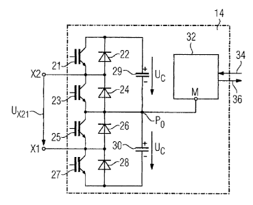
Figure 4 shows in greater detail the equivalent circuit of a first embodiment
of a
subsystem 14 according to the invention. This two-terminal subsystem 14
according
to the invention comprises four turn-off capable semiconductor switches
21, 23, 25 and 27, four diodes 22, 24, 26 and 28, two unipolar capacitors 29
and 30
and one electronic circuit 32, also referred to below as an electronic module
32. The
four turn-off capable semiconductor switches 21, 23, 25 and 27 are
electrically
connected in series. A diode 22, 24, 26 and 28 is electrically connected in
antiparallel with each of these semiconductor switches 21, 23, 25 and 27. One
unipolar capacitor 29 or 30 respectively is electrically connected in parallel
with each
pair of turn-off capable semiconductor switches 21, 23 or 25, 27 respectively.
The
unipolar capacitor 29 or 30 of this subsystem 14 comprises either one
capacitor or a
capacitor bank containing a plurality of such capacitors having a resultant
capacitance Co. The junction between the two turn-off capable semiconductor
switches 21 and 23 and the two diodes 22 and 24 form a second connecting
terminal
X2 of the subsystem 14. The junction between the two turn-off capable
semiconductor switches 25 and 27 and the two diodes 26 and 28 form a first
connecting terminal X1 of this subsystem 14. The junction between the emitter
of the
turn-off capable semiconductor switch 23, the collector of the turn-off
capable
semiconductor switch 25, the anode of the diode 24, the cathode of the diode
26, the
negative terminal of the unipolar capacitor 29 and the positive terminal of
the unipolar
capacitor 30 forms a common potential Po, which is electrically connected to a
reference-potential terminal M of the electronic module 32. This electronic
module 32
is linked to a higher-level converter controller (not shown in greater detail)
by two
optical fibers 34 and 36 in a manner allowing signal transmission.
CA 02620441 2008-02-27
PCT/EP2006/064925 - 8 -
WO 2007/025828
The common potential Po is used as the reference potential for
the electronic module 32. The fundamental principle in
selecting reference potentials is to select those potentials
that do not produce unnecessarily high voltage stresses for
driver chips of the turn-off capable semiconductor switches 21,
23, 25 and 27 or of the module packages for these turn-off
capable semiconductor switches 21, 23, 25 and 27.
This subsystem 14 according to the invention can be driven into
four control states I, II, III and IV. In control state I, the
turn-off capable semiconductor switches 21 and 25 are switched
on, and the turn-off capable semiconductor switches 23 and 27
are switched off. As a result, a terminal voltage Ux21 across
the connecting terminals X2 and X1 of the subsystem 14 equals
the capacitor voltage Uc across the capacitor 29. In control
state II, the turn-off capable semiconductor switches 21 and 27
are switched on, whereas the turn-off capable semiconductor
switches 23 and 25 are switched off. The terminal voltage Uxn
of the subsystem 14 now equals the sum of the capacitor
voltages Uc across the unipolar capacitors 29 and 30. In
control state III, the turn-off capable semiconductor
switches 23 and 25 are switched on and the turn-off capable
semiconductor switches 21 and 27 are switched off. In this
control state, the terminal voltage Ux21 of the subsystem 14
equals zero. In control state IV, the turn-off capable
semiconductor switches 23 and 27 are switched on, whereas the
turn-off capable semiconductor switches 21 and 25 are switched
off. As a result, the terminal voltage Ux21 of the subsystem 14
changes from potential level "zero" to potential level
"capacitor voltage Uc", which lies across the unipolar
capacitor 30. In control state I or IV, the energy store 29 or
30 receives or releases energy depending on a current direction
across the terminals. In control state II, the capacitors 29
and 30 receive or release energy depending on a current
direction across the terminals. In a control state III
("zero"), the energy in the capacitors 29 and 30 remains
CA 02620441 2008-02-27
PCT/EP2006/064925 - 8a -
WO 2007/025828
constant. Hence, in terms of functionality, this subsystem 14
according to the invention is equivalent to connecting in
series the known subsystem 11 and the known subsystem 12.
CA 02620441 2008-02-27
PCT/EP2006/064925 - 9 -
WO 2007/025828
In contrast, however, this subsystem 14 according to the
invention does not have the disadvantages of such a series
connection.
When the two known subsystems 11 and 12 are connected in
series, each subsystem 11 and 12 also has its own reference
potential and its own electronic module. If only one of these
two electronic modules is to be used, and the power for this
electronic module is only to be tapped from one corresponding
capacitor, the power is tapped asymmetrically and creates
asymmetries in the voltage division. In addition, a greater
outlay must be made for electrical isolation for driving the
turn-off capable semiconductor switches and acquiring the
capacitor voltages. These disadvantages no longer arise with
the two-terminal subsystem 14 embodied according to the
invention.
Figure 5 shows an equivalent circuit of a second embodiment of
a two-terminal subsystem 16 according to the invention. This
subsystem 16 differs from the subsystem 14 shown in Figure 4 in
that just pairs of turn-off capable semiconductor switches 21,
23 and 25, 27 are electrically connected in series. As in
subsystem 14, a diode 22, 24, 26 and 28 is electrically
connected in antiparallel with each turn-off capable
semiconductor switch 21, 23, 25 and 27. A respective unipolar
capacitor 29 or 30 is electrically connected in parallel with
each series connection. The junction between the emitter of the
turn-off capable semiconductor switch 23, the anode of the
diode 24 and the negative terminal of the unipolar capacitor 29
is electrically connected to a junction between the two turn-
off capable semiconductor switches 25, 27 that are
electrically connected in series. This junction forms a common
potential Po, to which the reference-potential terminal M of
the electronic module 32 is electrically connected. In
addition, the junction between the emitter of the turn-off
CA 02620441 2008-02-27
PCT/EP2006/064925 - 9a -
WO 2007/025828
capable semiconductor switch 27, the anode of the diode 28 and
the negative terminal of the unipolar capacitor 30
CA 02620441 2008-02-27
PCT/EP2006/064925 - 10 -
WO 2007/025828
forms the connecting terminal X1 of the subsystem 16. Hence, in
terms of functionality, this embodiment of the two-terminal
subsystem 16 is equivalent to connecting in series the two
known subsystems 11. Instead of using the negative terminal of
the capacitor 29 as the reference potential for the electronic
module 32, other terminals can also be used as the reference
potential. The fundamental principle in selecting reference
potentials is to select those potentials that do not produce
unnecessarily high voltage stress for the driver chips of the
turn-off capable semiconductor switches 21, 23, 25 and 27 or of
their module packages.
In a third embodiment of the two-terminal subsystem 18
according to the invention, in the same way as in the subsystem
16 shown in Figure 5, pairs of turn-off capable semiconductor
switches 21, 23 and 25, 27 are electrically connected in
series. Unlike the subsystem 16, the junction between the two
turn-off capable semiconductor switches 21 and 23 that are
electrically connected in series is now electrically connected
to a junction between the collector of the turn-off capable
semiconductor switch 25, the cathode of the diode 26 and the
positive terminal of the capacitor 30. The junction between the
two turn-off capable semiconductor switches 25 and 27 that are
electrically connected in series now forms a first connecting
terminal X1, whereas the junction between the collector of the
turn-off capable semiconductor switch 21, the cathode of the
diode 22 and the positive terminal of the capacitor 29 forms a
second connecting terminal X2 of this subsystem 18. As in the
subsystem 16, the negative terminal of the unipolar capacitor
29 is again provided as the reference potential for the
electronic module 32 of this subsystem 18. In terms of
functionality, this subsystem 18 is equivalent to connecting in
series the two known subsystems 12.
In the two-terminal subsystem 20 corresponding to the
equivalent circuit shown in Figure 7, once again, pairs of the
CA 02620441 2008-02-27
PCT/EP2006/064925 - 10a -
WO 2007/025828
four turn-off capable semiconductor switches 21, 23 and 25, 27
are electrically connected in series,
CA 02620441 2008-02-27
PCT/EP2006/064925 - 11 -
WO 2007/025828
with a diode 22, 24, 26 and 28 being electrically connected in
antiparallel with each turn-off capable semiconductor switch
21,...,27. A respective capacitor 29 or 30 is electrically
connected in parallel with a series connection of the turn-off
capable semiconductor switches 21, 23 or 25, 27. The junction
between the two turn-off capable semiconductor switches 21 and
23 that are electrically connected in series is electrically
connected to the junction between the two turn-off capable
semiconductor switches 25 and 27 that are electrically
connected in series. The junction between the collector of the
turn-off capable semiconductor switch 21, the cathode of the
diode 22 and the positive terminal of the capacitor 29 forms a
second connecting terminal X2 in this subsystem 20. The
junction between the emitter of the turn-off capable
semiconductor switch 27, the anode of the diode 28 and the
negative terminal of the capacitor 30 forms a first connecting
terminal X1 of the subsystem 20. In terms of functionality,
this subsystem 20 is equivalent to connecting in series a known
subsystem 12 with a known subsystem 11.
By means of this embodiment according to the invention of the
subsystems 14, 16, 28 and 20 for a converter circuit for high
voltages, in particular in the field of drive technology and
power engineering, the number of optical fibers between a
converter circuit, comprising a multiplicity of series-
connected subsystems, and a higher-level converter controller,
is halved compared with a known converter circuit for high
voltages. Each subsystem can be driven in such a way that a
terminal voltage Umi appears across its connecting terminals
X2, X1 that can assume four different potential levels. Such a
terminal voltage Ux21 can only be achieved with conventional
subsystems 11 and 12 if two series-connected subsystems 11, 12
or 12, 12 or 11, 11 or 12, 11 are used. Compared with merely
connecting in series two known subsystems 11 and 12, with these
being housed in one module, the subsystem 14 or 16 or 18 or 20
according to the invention requires just one electronic module
CA 02620441 2008-02-27
PCT/EP2006/064925 - lla -
WO 2007/025828
32, and, in addition, its power can be supplied symmetrically
from the capacitors 29 and 30.
CA 02620441 2008-02-27
PCT/EP2006/064925 - 12 -
WO 2007/025828
As a result, no further outlay is required for electrical
isolation for the drive and for acquiring a capacitor voltage
Uc.