Note: Descriptions are shown in the official language in which they were submitted.
CA 02620457 2008-11-21
1 0267-
2159PCT
CIRCUIT INTERRUPTING DEVICE WITH AUTOMATIC TEST
BACKGROUND
1. Field
The present application is directed to resettable circuit interrupting devices
including
without limitation ground fault circuit interrupters (GFCI's), arc fault
circuit interrupters
(AFCI's), immersion detection circuit interrupters (IDCI's), appliance leakage
circuit
interrupters (ALCI's), equipment leakage circuit interrupters (ELCI's),
circuit breakers,
contactors, latching relays and solenoid mechanisms.
CA 02620457 2011-08-24
2 0267-
2159PCT
2. Descrintion of the Related Art
Many electrical wiring devices have a line side, which is connectable to an
electrical
power supply, and a load side, which is connectable to one or more loads and
at least one
conductive path between the line and load sides. Electrical connections to
wires supplying
electrical power or wires conducting electricity to the one or more loads are
at line side and
load side connections respectively. The electrical wiring device industry has
witnessed an
increasing call for circuit breaking devices or systems which are designed to
interrupt power
to various loads, such as household appliances, consumer electrical products
and circuits or
systems branching from the device. In particular, electrical codes require
electrical circuits in
home bathrooms and kitchens to be equipped with ground fault circuit
interrupters (GFCI), for
example. Presently available GFCI devices, such as the device described in
commonly
=owned U.S. Pat. No. 4,595,894, use
an electrically activated trip mechanism to mechanically break an electrical
connection
between the line side and the load side. Such devices are resettable after
they are tripped by,
for example, the detection of a ground fault. In the device discussed in the
'894 patent, the trip
mechanism used to cause the mechanical breaking of the circuit (i.e., the
conductive path
between the line and load sides) includes a solenoid (or trip coil). A test
button is used to test
the trip mechanism and circuitry used to sense faults, and a reset button is
used to reset the
electrical connection between line and load sides.
Over the years circuit interrupting devices have evolved to include circuit
interrupting
devices with a reset lock-out function intended to prohibit devices with, for
example, an
inoperable circuit interrupting portion (i.e., fault sensing circuit and trip
mechanism), an open
neutral condition, or a reverse wiring condition, from being reset. Commonly
owned U.S. Pat.
No. 6,040,967, (hereinafter " the "967 patent)
describes a family of resettable circuit interrupting devices capable of
locking out
the reset portion of the device if the circuit interrupting portion (referred
to as the "circuit
interrupter in the '967 patent) is non-operational or if an open neutral
condition exists.
Commonly owned U.S. Pat. No. 6,246,558,
describes a family of resettable circuit interrupting devices capable of
locking out
the reset portion of the device if a reverse wiring condition exists.
CA 02620457 2008-11-21
3 0267-
2159PCT
While most, if not all, existing circuit interrupting devices meet existing
standards
governing electrical fault protection devices, there are indications that next
generation
standards may require circuit interrupting devices capable of permanently
interrupting the
power supplied to the load side of the device in the event the device is no
longer capable of
operating according to applicable standards. Further, next generation
standards may require
automatic testing of the trip mechanism of the device and permanently
interrupting the power
supplied to the load side of the device in the event the device is no longer
capable of operating
according to applicable standards.
CA 02620457 2008-11-21
4 0267-
2159PCT
SUMMARY
The present disclosure relates to resettable circuit interrupting devices
having self-test
and permanent power interrupting systems. The permanent power interrupting
system is
activated when a circuit interrupting device experiences a device malfunction.
The device
malfunction refers to circumstances and/or conditions where the circuit
interrupting device of
the present invention is unable to operate in accordance with applicable
standards governing
the device and/or is unable to operate in accordance with its design
characteristics.
In one embodiment the circuit interrupting devices includes a phase conductive
path
and a neutral conductive path each conductive path having a line side and a
load side. A fault
sensor is provided to monitor the phase and neutral conductive paths for a
fault condition and
said fault sensor outputs a condition signal in the event a fault condition is
detected. Thus, the
condition signal indicates that a fault condition has been detected. The fault
condition can be
a ground fault, an arc fault, an appliance leakage fault, an immersion fault
or the results of a
test of some or all of the circuit interrupting portion. A relay controller
coupled to a relay is
provided and said relay controller is configured to receive the condition
signal. In this
configuration, when the relay controller receives the condition signal the
relay controller
energizes the relay causing electrical discontinuity in the phase and neutral
conductive paths
between the line side and load side. A sensor is provided for monitoring the
load side of the
circuit interrupting device. For example, a load voltage sensor can be
provided to measure the
voltage between the phase and neutral conductive paths at the load side and to
output a
voltage signal in response to the measured voltage; this measured voltage
signal is generally
referred to as a monitoring signal. The power interrupting system is provided
to cause
permanent or non-resettable electrical discontinuity in the conductive paths
in response to the
detection of a device malfunction. In general, the device malfunction is
detected based upon
the condition signal and the monitoring signal. Examples of device
malfunctions include the
improper operation of all or a part of the fault sensing circuitry, improper
operation of all or a
part of the mechanical components of the circuit interrupting device, e.g, a
faulty solenoid or
fused contacts, or the improper operation of all or a part of the support
circuitry for the circuit
interrupting device, e.g., the self-test system or controllers.
CA 02620457 2008-11-21
0267-2159PCT
The power interrupting system includes a power interrupting controller and a
power
interrupter capable of causing the permanent electrical discontinuity in the
phase and neutral
conductive paths between the line side and load side. Preferably, the power
interrupter
includes a fuse assembly (e.g., at least one fusible link) thermally coupled
to a heater
assembly (e.g., at least one heating element). The power interrupting
controller may be a
switching network, or a combination of a switching network and condition test
logic circuitry
(or a microcontroller or microprocessor) capable of receiving inputs from a
plurality of
sensors, processing said inputs and activating the switching network in
response to the inputs
from the plurality of sensors.
The circuit interrupting device may further include a self-test system capable
of
automatically inducing a fault condition into the fault sensor or inducing
conditions that
typically result when a fault occurs (e.g., a current imbalance between phase
and neutral
conductors when a ground fault occurs).
In an alternative embodiment, the circuit interrupting device includes a
housing, and a
phase conductive path and a neutral conductive path each disposed at least
partially within the
housing between a line side and a load side. Preferably, the phase conductive
path terminates
at a first connection capable of being electrically connected to a source of
electricity, a second
connection capable of conducting electricity to at least one load and a third
connection
capable of conducting electricity to at least one user accessible load.
Similarly, the neutral
conductive path terminates at a first connection capable of being electrically
connected to a
source of electricity, a second connection capable of providing a neutral
connection to the at
least one load and a third connection capable of providing a neutral
connection to the at least
one user accessible load. The device also includes a circuit interrupting
portion disposed
within the housing and configured to cause electrical discontinuity in the
phase and neutral
conductive paths between the line side and the load side upon the occurrence
of a fault
condition. The fault condition can be a ground fault, an arc fault, an
appliance leakage fault,
an immersion fault or the result of a test of a part of or all of the circuit
interrupting portion.
A power interrupting system is also disposed within the housing and configured
to cause
permanent or non-resettable electrical discontinuity in the phase and neutral
conductive paths
between the line side and the load side upon the occurrence of a device
malfunction.
CA 02620457 2008-11-21
6 0267-
2159PCT
BRIEF DESCRIPTION OF THE DRAWINGS
Preferred embodiments of the present application are described herein with
reference
to the drawings in which similar elements are given similar reference
characters, wherein:
FIG. 1 is a perspective view of a circuit interrupting device (implemented as
a GFCI)
constructed in accordance with the present invention;
FIG. 2 is a schematic representation of one embodiment of the circuit
interrupting
device of the present invention having a power interrupting system and an
optional automatic
self-test system;
FIG. 3 is a schematic representation of one embodiment of a fault sensor and
relay
controller for detecting ground faults and resetting the device of Fig. 2;
FIG. 3A is a schematic representation of FIG. 3 with a self test system;
FIG. 4 is a schematic representation of one embodiment of a power interrupting
system for disconnecting power to the load side of the GFCI device of Fig. 2;
FIG. 4A is a schematic representation of an alternative embodiment of a power
interrupting system for disconnecting power to the load side of the GFCI
device of Fig. 2;
FIG. 5 is a schematic representation of yet another alternative embodiment of
a power
interrupting system for disconnecting power to the load side of the device of
Fig. 2;
FIG. 5A is a schematic representation of a further alternative embodiment of a
power
interrupting system for disconnecting power to the load side of the device of
Fig. 2;
FIG. 6 is a schematic representation of a further alternative embodiment of a
power
interrupting system for disconnecting power to the load side of the device of
Fig. 2;
FIG. 7 is a schematic representation of a further alternative embodiment of a
power
interrupting system for disconnecting power to the load side of the device of
Fig. 2;
FIG. 8 is a schematic representation of an embodiment of a circuit
interrupting device
with a power interrupting system and an optional automatic self-test feature;
FIG. 9 is a schematic representation of yet another embodiment of a circuit
interrupting device with a power interrupting system and an optional automatic
self-test
system;
FIG. 10 is an exemplary flow diagram for the operation of the different
exemplary
embodiments of the power interrupting system controllers.
CA 02620457 2008-11-21
7 0267-
2159PCT
DETAILED DESCRIPTION OF EMBODIMENTS
The present disclosure contemplates various types of circuit interrupting
devices that
are capable of breaking at least one conductive path at both a line side and a
load side of the
device. The conductive path typically has at least a first end (i.e., the line
side) that connects
to a source of electrical power and at least a second end (i.e., the load
side) that connects to
one or more loads. As noted, the various devices in the family of resettable
circuit
interrupting devices include: ground fault circuit interrupters (GFCI's), arc
fault circuit
interrupters (AFCI's), immersion detection circuit interrupters (IDCI's),
appliance leakage
circuit interrupters (ALCI's) and equipment leakage circuit interrupters
(ELCI's).
For the purpose of the present disclosure, the structure, mechanisms or
systems used in
the circuit interrupting devices, shown in the drawings and described
hereinbelow, are
incorporated into a GFCI receptacle suitable for installation in a single-gang
junction box used
in, for example, a residential electrical wiring system. However, the
mechanisms and systems
according to the present disclosure can be included in any of the various
devices in the family
of resettable circuit interrupting devices.
The GFCI receptacles described herein have line, load and user accessible
phase
connections, line, load and user accessible neutral connections. The load and
user accessible
connections permit external conductors or appliances to be connected to the
device and the
line connections permit electrical connection to a source of electricity;
these connections may
be implemented, for example, with electrical fastening devices that secure or
connect external
conductors to the circuit interrupting device, as well as conduct electricity.
Examples of such
connections include binding screws, lugs, terminals and external plug
connections.
The circuit interrupting and reset portions described herein preferably use
electro-
mechanical components to break (open) and make (close) one or more conductive
paths
between the line and load sides of the device. However, electrical components,
such as solid
state switches, semiconductor components, integrated circuits and other
supporting circuitry,
may be used to open and close the conductive paths.
Generally, the circuit interrupting portion is used to automatically break
electrical
continuity in one or more conductive paths (i.e., open the conductive path)
between the line
and load sides upon the detection of a fault, which in the particular
embodiments described is
CA 02620457 2011-08-24
8 0267-
2159PCT
a ground fault. The reset portion is used to close the open conductive paths.
In the
embodiments including a reset lockout, the reset portion is used to close the
open conductive
paths when allowed by the reset lockout. In this configuration, the operation
of the reset and
reset lockout portions is in conjunction with the operation of all or part of
the circuit
interrupting portion, so that electrical continuity in open conductive paths
cannot be reset if all
or part of the circuit interrupting portion is non-operational, if an open
neutral condition exists
and/or if the device is reverse wired. It should be noted that the disclosure
is not limited to
embodiments where all of the circuit interrupting portion is activated by
depressing the reset
button for devices with the reset lockout feature. That is, all or a part of
the circuit
interrupting portion can be activated when the reset button is depressed and
the reset lockout
will prevent the device from being reset if the activated portion is not
operating properly.
Therefore, the present disclosure also contemplates embodiments where a
portion of the
circuit interrupting portion is used in conjunction with the reset or reset
lockout portions.
In an alternative embodiment, the circuit interrupting devices may also
include a trip
portion that operates independently of the circuit interrupting portion so
that in the event the
circuit interrupting portion becomes non-operational the device can still be
tripped.
Preferably, the trip portion is manually activated and uses mechanical
components to break
one or more conductive paths. However, the trip portion may use electrical
circuitry and/or
electro-mechanical components to break either the phase or neutral conductive
path or both
paths.
The above-described features can be incorporated in any resettable circuit
interrupting
device, but for simplicity the descriptions herein are directed to GFCI
receptacles. A more
detailed description of a GFCI receptacle is provided in U.S. Pat. Nos.
4,595,894; 6,437,700;
6,040967 and 6,246,558
It should also be noted that binding screws are exemplary of the types of
wiring
terminals that can be used to provide the electrical connections. Examples of
other types of
wiring terminals include set screws, pressure clamps, pressure plates, push-in
type
connections, pigtails and quick-connect tabs.
Turning now to FIG. 1, the exemplary GFCI device 10 shown is a GFCI receptacle
having a housing 12 consisting of a relatively central body 14 to which a face
or cover portion
16 and a rear portion 18 are removably secured. The face portion 16 has entry
ports 20 for
receiving normal or polarized prongs of a male plug of the type normally found
at the end of a
CA 02620457 2008-11-21
9 0267-
2159PCT
cord for an appliance (e.g., a lamp), as well as ground-prong-receiving
openings 22 to
accommodate a three-prong plug. The receptacle also includes a mounting strap
24 used to
fasten the receptacle to a junction box.
A reset button 30 forming a part of a reset mechanism extends through opening
32 in
the face portion 16 of the housing 12. The reset button is used to reestablish
electrical
continuity between the input and output conductive paths or conductors. A test
button 26
extends through opening 28 in the face portion 16 of the housing 12. The test
button is used
to manually activate a test cycle, which test the operation of all or part of
a circuit interrupting
portion of the device.
Electrical connections to existing household electrical wiring are made via
binding
screws 34 and 36, where screw 34 is an input (or line) connection point and
screw 36 is an
output (or load) connection point. It should be noted that two additional
binding screws (not
shown) are located on the opposite side of the receptacle 10. Similar to
binding screws 34 and
36, these additional binding screws provide input and output connection
points. Further, the
input connections are for line side phase (hot) and neutral conductors of the
household wiring,
and the output connections are for load side phase (hot) and neutral
conductors of the
household wiring. The plug connections are also considered output conductors.
The circuit
interrupting portion, to be described in more detail below, is used to break
electrical continuity
between input (line) and output (load) conductive paths (or conductors).
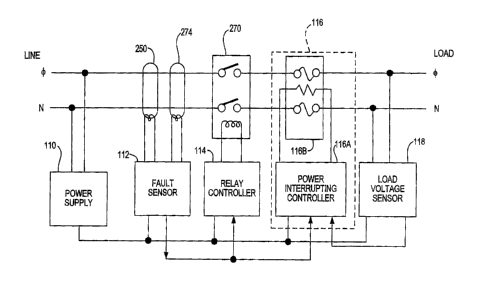
Referring to FIG. 2, a block diagram of the electrical components of a GFCI
device
with a circuit interrupting system and optional automatic self-test system is
shown. In this
embodiment, the device includes a power supply 110 connected to the line side
phase and
neutral conductors, that utilizes known techniques to convert AC line voltage
to DC power
suitable for supplying power to the fault sensor 112, relay controller 114,
power interrupting
controller 116A and load voltage sensor 118. It should be noted that the fault
sensor 112,
relay controller 114 and relay 270 are associated with the circuit
interrupting portion of the
device.
In one embodiment, the fault sensor 112 utilizes a pair of differential
transformers 250
and 274 that monitors the AC phase and neutral conductors for ground fault
conditions and
generates control signals to relay controller 114 and to power interrupting
controller 116 in the
event a ground fault condition is detected or a self-test cycle is performed.
For example, if a
ground fault condition is detected by fault sensor 112, a signal is sent to
relay controller 114
CA 02620457 2008-11-21
0267-2159PCT
causing the controller 114 to energize relay 270 thus opening the conduction
path (causing
electrical discontinuity) between the line side and load side phase and
neutral conductors.
One implementation of the fault sensor 112, relay controller 114 and relay 270
is
shown in FIG. 3. However, other implementations of the fault sensor, relay
controller and
relay are also contemplated. Referring to FIG. 3, a schematic representation
of conventional
circuitry for the fault sensor 112 used to detect fault conditions, here
ground faults, and relay
controller 114 and relay 270 are used to open the phase and neutral conductive
paths in the
event a ground fault is detected. Typically, the fault sensor uses a
differential transformer and
neutral transformer to sense ground faults and energize a relay that
disconnects power to the
load side in the event a ground fault is detected. The circuit of FIG. 3 is
for single phase
applications with 120 volts line to ground, is exemplary of a fault sensor 112
and relay
controller 114, and operates in the following manner:
For phase to neutral fault detection, differential transformer 250 monitors
the flow of
current in the line side phase and neutral conductors, 252 and 254,
respectively, and produces
in its secondary winding a fault or condition signal when the current flowing
in the phase
conductor (or conductors) 252 does not equal the current flowing in the
neutral conductor 254.
The output from the secondary of differential transformer 250 (i.e., the
condition signal) is
conveyed to integrated circuit 256 through diode 258, capacitors 260, 262 and
264, and
resistor 266. Integrated circuit 256 may be a type LM 1851 Ground Fault
Interrupter
manufactured by National Semiconductor Corporation. Diode 258 and resistor 266
are
arranged so as to promote quick discharge of capacitor 260. This discharge of
capacitor 260
allows integrated circuit 256 to be kept continuously energized and thus
considerably reduces
the time required for detection of a fault. Continuous energization of
integrated circuit 256
from the line side is made possible by capacitor 268 which is attached to
output pin 7 of
integrated circuit 256, which basically controls the trip circuit while
minimizing burnout of
the trip coil 270.
For neutral to ground fault detection (otherwise referred to as a ground
neutral
condition), the fault sensor 112 functions similarly to the phase to neutral
fault detection
described above. Transformer 274 (together with differential transformer 250)
form part of an
induction coil that has a signal induced on its secondary windings that is
carried through
capacitors 276 and 278 to input pin 4 of integrated circuit 256. This induced
signal is another
type of a condition signal indicating to integrated circuit 256 that a ground
neutral condition
CA 02620457 2008-11-21
11 0267-
2159PCT
has been detected and that the device should be tripped. Thus, at least two
types of ground
faults can be detected by the circuit diagram shown in FIG. 3: phase to
neutral fault and a
neutral to ground fault.
The trip circuit for both types of faults is identical in that if a fault
(ground fault or
ground neutral condition) is detected by the input pins 2, 3, and 4 of IC 256,
a signal is output
from pin 7 of integrated circuit 256 causing capacitor 268 to charge. The
signal from pin 7 of
integrated circuit 256 is applied to the gate of SCR 272 causing said SCR to
conduct causing
current to flow through coil 270 thus energizing coil 270. Coil 270 is part of
a relay which
includes a plunger (not shown) and when coil 270 is energized, the plunger is
caused to move
to engage movable arms to disconnect the line (phase and neutral ) conductors
from the load
(phase and neutral) conductors. In particular, upon energization of coil 270,
contacts 300 and
302 of the ground fault circuit interrupter are opened which in turn
disconnects power to the
load side phase and neutral conductors 304 and 306.
The fault sensor 112 may include a push-button 308 and resistor 310 as part of
a self-
test system that induces a ground fault condition (i.e., a current imbalance
is caused) onto the
line side conductors for detection by the fault sensor 112. Alternatively or
in addition to push
button 308, a self-test system 309 (seen in FIG. 3A) can be incorporated into
the fault sensor
112. The self test system uses TEST button 308 for manual activation of the
self test.
However, the self-test system 309 is preferably configured to periodically
output a test signal
through resistor 310 to induce a ground fault condition onto the line side
conductors for
detection by the fault sensor 112, thus permitting automatic testing of all or
part of the circuit
interrupting portion. The self-test system may be a clocking circuit
configured to output a test
signal, for example, once a day, once a week, or once a month. When all or
part of the fault
sensor circuitry is tested the device is typically set in a tripped state. As
a result, the device
would need to be reset. The device can then be manually reset using the reset
button, or and
automatic reset operation could be performed where a reset signal is generated
causing the
line and load side connections to be reestablished. Since the timing of the
self-test may be
inconvenient, i.e., when the device is in use, it may be desirable to have the
self-test system
send a signal to the relay controller 114 to cause the relay 124 to close
immediately after it has
been opened by the detection of the simulated fault induced by the self-test
system. If a self-
test is activated when, for example, the device is in use, it is preferable
that the self-test cycle
and reset time is fast enough so that a human would not notice the brief
disruption of power
= CA 02620457 2011-08-24
12
0267-2159PCT
provided to the load. That is, the time between the energizing of the relay
270 to open the
conductive paths between line and load phase and neutral conductors and the
time the relay
closes the conductive paths between line and load phase and neutral conductors
is sufficiently
small that the disruption in power provided to any load is not significant
(i.e., will not
adversely affect the operation of the connected load) or detectable by a
human.
It should be noted that in the event the circuit interrupting device is a
reset lock-out
type circuit interrupting device, resetting of the device is prevented if all
or any portion of the
circuit interrupting portion (i.e., fault sensor 112, differential
transformers 250 and 274, relay
controller 114 and relay 270) is not functioning properly, or if all or any
portion of the relay
controller or relay are not functioning properly, or if both the fault sensor
and relay controller
and relay are not functioning properly. Examples of reset lockout type circuit
interrupting
devices are described in commonly owned US Patent Nos. 6,040,967; 6,381,112;
6,657,834
and 6,671,145 .
Referring again to FIG. 2, the circuit interrupting device according to the
present
disclosure may include a power interrupting system 116 capable of causing
permanent
electrical discontinuity in the conductive paths (i.e., opening the conductive
paths) between
the line side phase and neutral conductors and the load side phase and neutral
conductors in
the event one or more device malfunctions exist. The power interrupting system
116 includes
a controller 116A and a power interrupter 116B. In the embodiment of FIG. 2,
the controller
116A receives signals from the fault sensor 112 and load voltage sensor 118
and uses logic
circuitry to determine whether or not one or more device malfunctions exist.
In the event one
or more device malfunctions is detected the power interrupter 116B is
activated by controller
116A to cause all or a part of the power interrupting system to become
disabled and thus cause
non-resettable electrical discontinuity in the phase and neutral conductive
paths preventing
power distribution to the load side of the circuit interrupting device 10.
The power interrupting system 116 will be described with reference to the
various
exemplary embodiments depicted in FIGS. 4-7. In the embodiment of FIG. 4, the
power
interrupting controller 116A includes condition testing logic circuit 400
capable of receiving
inputs from either the fault sensor 112, the load voltage sensor 118 (seen in
FIG. 2) or both.
For example, the gate input of SCR 272 (seen in FIG. 3 and shown as
originating from pin 7
of IC 256) on which the trip signal is received and is used to energize relay
270 could be
inputted to the condition test logic circuit 400. The output of the condition
testing logic is
CA 02620457 2011-08-24
13
0267-2159PCT
transferred to switching assembly 401 including transistor 402, biasing
resistors 404 and 406
and rectifying diode 408. Here the output of the condition testing logic is
transferred to the
base of transistor 402. If the gate input of SCR 272 is used as the input to
the condition test
= logic circuit 400, and the SCR is activated beyond its design time
period, which may be
indicative of a device malfunction, the power interrupter 116B may be
sufficiently activated to
cause all or a part of the power interrupter to become disabled, thus causing
non-resettable
electrical discontinuity in the phase and neutral conductive paths and
preventing power
distribution to the load side of the circuit interrupting device 10. It should
be noted that an
SCR or Triac could be used for the switching assembly 401 as shown in FIG. 5.
Continuing with FIG. 4, the power interrupter 116B includes a fuse assembly,
e.g.,
thermal fusible links 410 and 412, connected in series with the phase and
neutral conductive
paths as shown, and heater assembly 414 thermally coupled to the fuse
assembly. In this
configuration, when energy is supplied to the heater assembly heat is
transferred to the fuse
assembly, here the fusible links. When sufficient heat energy is transferred
to the fuse
assembly to cause the fuse assembly to open, non-resettable or limited
resettable electrical
discontinuity in the phase and neutral conductive paths occurs. As a result,
power to the load
side of the circuit interrupting device is removed.
The fusible links could be, for example, lengths solder or other material that
when
heated to a certain temperature open or otherwise break the respective
conductive path. The
fusible links may also include thermal fuses, thermally activated switches, a
muscle wire
formed of, for example, a material described in Appendix A (attached to this
application
) and other thermally responsive devices and/or
materials capable of changing their shape, length or overall structure when
subjected to a
certain amount of heat. It should be noted that in instances where a thermally
responsive
material is used as the fusible link having characteristics of breaking the
conductive paths
when heated and reestablishing the conductive paths when cooled, the
electrical discontinuity
in the conductive path is a limited resettable electrical discontinuity. It
should also be noted
that non-thermal fusible links are also contemplated by the present
disclosure.
Further, thermally responsive materials can be incorporated in a circuit
interrupting
device and more particularly interfaced with the circuit interrupting portion
of a circuit
interrupting device (activated with a TEST button) or interfaced with the
reset mechanism of
the circuit interrupting device (activated with a RESET button) ¨for circuit
interrupting
=
=
=
CA 02620457 2011-08-24
14 0267-
2159PCT
devices having the reset lockout feature or for devices that do not have the
reset lockout
feature. As shown in Appendix B attached to this application and which is
incorporated
herein by reference, a material such as Flexinol (shape memory alloy) can be
coupled to the
reset mechanism (including a reset button) of a circuit interrupting device
shown in FIG. 1
(such a device is disclosed in an application titled Circuit Interrupting
Device and System
Utilizing Bridge Contact having serial no. 10/690,776, .
1 so that the expansion or contraction of these materials when subjected to a
threshold amount of heat will change their shape accordingly to interact with
the TRIP button
causing the circuit interrupting device to trip or interact with the reset
button causing the
circuit interrupting device to reset which automatically tests all or part of
the circuit
interrupting portion when the circuit interrupting device has the reset
lockout feature.
The heater assembly 414 could include the solenoid (e.g., trip coil 270)
provided with
conventional circuit interrupting devices and used to open and close the
conductive paths that
perform the circuit interrupting operation of the device. If the solenoid is
used as the heater
assembly 414, sufficient heat is generated when the solenoid is activated for
a period of time
that exceeds the normal time needed to trip the circuit interrupting device.
Alternatively, the
heater assembly 414 may be a heating element, e.g. a resistor.
On embodiment is to connect a heating element such as a resistor in parallel
with the
solenoid. This heater would act on an expanding or contracting material in
such a manner that
the time required to cause a reaction is greater than the maximum allowable
trip time of the
circuit interrupting device. The expansion and/or contraction would be able to
permanently
disable the device when such expanding material is engaged or coupled to at
least a portion of
the circuit interrupting portion.
Thermal coupling of the heater assembly to the fuse assembly could be achieved
by,
for example, wrapping solder lengths (the fuse assembly) around one or more
resistors acting
as the heater assembly 414.
In operation, when the output signal from the condition testing logic 400 is
sufficient
to turn on transistor 402 current will flow through the heater assembly
heating the fusible links
until they open the respective conductive path. If the fusible links are
solder lengths, the
solder would melt when heated thus permanently opening the respective
conductive path. As
noted above, if a thermal responsive material is used as the fusible link
having characteristics
where when heated a break in a conductive path occurs and when cooled the
conductive path
CA 02620457 2008-11-21
15 0267-
2159PCT
is again made, the electrical discontinuity in the conductive path is a
limited resettable
electrical discontinuity.
In the embodiment of FIG. 5, the power interrupting controller 116A includes
condition testing logic 400 capable of receiving inputs from either the fault
sensor 112, or load
voltage sensor 118 (seen in FIG. 2) or both. The output of the condition
testing logic is
transferred to switch assembly 401 that includes triacs 420 and 422. The power
interrupter
116B includes a fuse assembly, e.g., thermal fusible links 410 and 412,
connected in series
with the phase and neutral conductive paths as shown, and heater assembly 414
thermally
coupled to the fuse assembly. In this configuration, when sufficient energy is
supplied to the
heater assembly the fuse assembly, here the fusible links, opens thus causing
permanent
electrical discontinuity in the phase and neutral conductive paths. As a
result, power to the
load side of the circuit interrupting device is removed. The fusible links can
be similar to
those described above. In this embodiment, the heater assembly includes two
heating
elements 416 and 418, e.g. resistors, where one heating element heats fusible
link 410 and the
other heats fusible link 412.
FIGS. 4A and 5A are similar to FIGS. 4 and 5 respectively, except that the
signal
supplied to the switch assembly, i.e., power interrupter and/or power
interrupting controller
comes from an external source, e.g., a controller or supervisory circuit
instead of a logic
circuit.
The embodiment of FIG. 6 is similar to the embodiment of FIG. 4, except that
microcontroller 430 provides the signal to the power interrupting controller
116A to cause the
power interrupter 116B to open the conductive paths as described above. In
this embodiment,
the microcontroller 430 can be used to initiate a self-test of the circuit
interrupting device
operation and in the event a device malfunction is detected by the
microcontroller 430 switch
assembly is activated causing the heater assembly to activate the fuse
assembly to open the
conductive paths. FIG. 7 is similar to FIG. 5 except that the switching
assembly includes
brownout protection. In this embodiment of controller 116A, microcontroller
430 provides an
output signal to transistor Q1 via capacitor Cl and resistor Rl. Transistor
Ql, which controls
when transistor Q4 can turn on, is provided to hold the voltage across
capacitor C2 to about
zero volts and is briefly turned on by the output signal from microcontroller
430. If the output
of the microcontroller 430 is left floating, or a short time after the output
of the
microcontroller is driven high or low, resistor R1 quickly bleeds capacitor Cl
thereby turning
CA 02620457 2008-11-21
16
0267-2159PCT
off transistor Ql. When transistor Q1 is off, transistor Q4 can turn on when
the voltage on the
phase conductive path overcomes the zener voltage of zener diode Z2, the diode
drop across
diode D2, and voltage across resistor divider R4/(R2+R3+R4). With transistor
Q1 off, voltage
= on the phase conductive path is free to charge capacitor C2 to the point
where transistor Q4
turns on and energize heater assembly 414. Energizing the heater assembly
takes place by
current flowing from the phase conductive path through the heater assembly
414, through
diode D4 and transistor Q4 to the neutral conductive path. Such current flow
occurs on
positive half-cycles due to diode D4 and when transistor Q4 is turned on.
Heater assembly 414
then begins to transfer heat energy to the fusible links 410 and 412, and in
the event the heat
energy transferred to the fusible links reaches the melting point of the
fusible link, then fusible
links will break causing electrical discontinuity in the conductive paths.
Referring now to FIG 8 an alternative embodiment of the circuit interrupting
device is
shown. In this embodiment, microcontroller 440 is connected to fault sensor
112, relay
controller 114 and power interrupting system 116 and is provided to perform a
self-test of the
fault sensor, relay controller and power interrupting system and determine if
one or more
device malfunctions exist and then activate the power interrupting system 116
to open the
conductive paths as described above.
Referring to FIG. 9, another alternative embodiment of the circuit
interrupting device
is shown. In this embodiment, microcontroller 450 is connected to fault sensor
112, fault
inducer 452, relay controller 114, power interrupting system 116 and load
voltage sensor 118,
and is provided to cause the fault inducer 452 to initiate a self-test of the
fault sensor, relay
controller, relay and power interrupting system and determine if one or more
device
malfunctions exist and then activate the power interrupting system to open the
conductive
paths as described above.
FIG. 10 provides an exemplary flow diagram for the operation of the
microcontroller
440 or 450.
As noted, although the components used during circuit interrupting and some
device
reset operations are electro-mechanical in nature, the present application
also contemplates
using electrical components, such as solid state switches and supporting
circuitry, as well as
other types of components capable or making and breaking electrical continuity
in the
conductive path.
While there have been shown and described and pointed out the fundamental
features
CA 02620457 2008-11-21
17 0267-
2159PCT
of the application, it will be understood that various omissions and
substitutions and changes
of the form and details of the device described and illustrated and in its
operation may be
made by those skilled in the art, without departing from the spirit of the
application.
CA 02620457 2008-11-21
18 0267-
2159PCT
Appendix A
THE SHAPE MEMORY EFFECT = Phenomenon, Alloys and Applications
Dieter Stoeckel
NDC * Nitinol Devices & Components, Inc.. Fremont, CA
Introduction
Certain metallic materials will, after an apparent plastic deformation, return
to their original
shape when heated. The same materials, in a certain temperature range, can be
strained up to
approx. 10% and still will return to their original shape when unloaded. These
unusual
effects are called thermal shape memory and superelasticity (elastic shape
memory)
respectively [1]. Both effects depend on the occurrence of a specific type of
phase change
known as thermoelastic martensitic transformation. Shape memory and
superelastic alloys
respond to temperature changes and mechanical stresses in non-conventional and
highly
amazing ways. They are, therefore, sometimes called "smart materials." The
shape memory
effect can be used to generate motion and/or force, while superelasticity
allows energy
storage. Both effects have fascinated scientists and engineers for almost
three decades,
drawing them to conferences seminars in great numbers. However, very few
developments
made it to the market, and can be considered economic successes. Recent
successes come
mainly from medical applications utilizing the superelasticity and
biocompatibility of Ni-Ti
alloys.
Shape Memory Effect
"Shape Memory" describes the effect of restoring the original shape of a
plastically deformed
sample by heating it. This phenomenon results from a crystalline phase change
known as
"thermoelastic martensitic transformation." At temperatures below the
transformation
temperature, shape memory alloys are martensitic. In this condition, their
microstructure is
characterized by "self-accommodating twins." The martensite is soft and can be
deformed
quite easily by de-twinning. Heating above the transformation temperature
recovers the
original shape and converts the material to its high strength, austenitic,
condition (Fig. 1).
CA 02620457 2008-11-21
19 0267-2159PCT
Appendix A
; . 44 = , ,,,,,, ..., . 1
* :
ILi
' iit4, 4. ===
_ .A._ .....iv.;..i: 7,::........:......-_-_,....tõ....
-*:
1
k
1
4Ittria:
1 4.40. war
I *****C
1 , ,.:,...,., 'V
>., _______________________________________________
Deformation
Fig. I : Scheolafic represeniation of ibe shape inetnoly effect and
superelasticity
The transformation from austenite to martensite and the reverse transformation
from
martensite to austenite do not take place at the same temperature. A plot of
the volume
fraction of martensite, or more practically, the length of a wire loaded with
a constant weight,
as a function of temperature provides a curve of the type shown schematically
in Figure 2.
The complete transformation cycle is characterized by the following
temperatures: austenite
start temperature (As), austenite finish temperature (Af), martensite start
temperature (Ms) and
martensite finish temperature (Mf).
If a stress is applied to a shape memory alloy in the temperature range
between Af and a
maximum temperature Md, martensite can be stress-induced. Less energy is
needed to stress-
induce and deform martensite than to deform the austenite by conventional
mechanisms. Up
to 10% strain can be accommodated by this process (single crystals of specific
alloys can
show as much as 25% pseudoelastic strain in certain directions). As austenite
is the
thermodynamically stable phase at this temperature under no-load conditions,
the material
springs back into its original shape when the stress is no longer applied.
This extraordinary
elasticity is also called pseudoelasticity or transformational
superelasticity.
It becomes increasingly difficult to stress-induce martensite at increasing
temperatures above
M. Eventually, it is easier to deform the material by conventional mechanisms
than by
inducing and deforming martensite. The temperature at which martensite is no
longer stress-
induced is called Md. Above Md, the alloys are deformed like ordinary
materials. Thus,
superelasticity is only observed over a narrow temperature range.
CA 02620457 2008-11-21
20 0267-
2159PCT
Appendix A
ktf
1104 ... = '
1.r: 1 4f
Zo=*.
TO,0
:
:11)1110M
*
41111111111111r*.
i
ms. '
r011ktnat** *Mita
Fig. 2 (lefl): :Schematic repreEe.tmal ion or the hysteresi; loop
Fig. 3 (right): curves at di Mrent ternperature
The design of shape memory components, e.g. fasteners or actuators, is based
on the distinctly
different stress/strain curves of the martensite and austenite, and their
temperature
dependence. Figure 3 shows tensile curves of a Ni-Ti alloy at various
temperatures. While
the austenitic curve (T>Md) looks like that of a "normal" material, the
martensitic one
(T<Mf) is quite unusual. On exceeding a first yield point, several percent
strain can be
accumulated with only little stress increase. After that, stress increases
rapidly with further
deformation. The deformation in the "plateau region" can be recovered
thermally.
Deformation exceeding a second yield point cannot be recovered. The material
is then
plastically deformed in a conventional way. At temperatures T>Af, again, a
plateau is
observed upon loading. In this case, it is Caused by stress induced
martensite. Upon
unloading, the material transforms back into austenite at a lower stress
(unloading plateau).
With increasing temperature, both loading and unloading plateau stress
increase linearly [2].
Shape Memory Alloys
The shape memory effect as the result of a martensitic transformation has been
known since
the mid 1950's, when the effect was discovered in copper base alloys. In the
early sixties,
researchers at the Naval Ordnance Laboratory found the shape memory effect in
Ni-Ti alloys
(Nitinol - Ni-Ti Naval Ordnance Lab). Today, these alloys are the most widely
used shape
memory and superelastic alloys, combining the most pronounced shape memory
effect and
superelasticity, corrosion resistance and biocompatibility, and superior
engineering properties.
Copper based alloys like Cu-Zn-AI and Cu-Al-Ni are commercially available,
too. These
CA 02620457 2008-11-21
21 0267-
2159PCT
Appendix A
alloys are less stable and more brittle than Ni-Ti, and therefore, although
less expensive, have
found only limited acceptance. In recent years, iron based shape memory alloys
have been
widely advertised. However, with their limited shape memory strain, lack of
ductility and
other essential properties, these alloys will have to prove themselves as
viable engineering
materials.
The transformation temperatures of shape memory alloys can be adjusted through
changes in
composition. Ni-Ti as well as Cu-Zn-Al alloys show transformation temperatures
between -
100 C and -I-100 C. Cu-Al-Ni alloys up to 200 C. Unfortunately, Cu-Al-Ni
alloys are not
stable in cyclic applications. Some ternary Ni-Ti-Pd [3], Ni-Ti-Hf and Ni-Ti-
Zr [4] alloys
also are reported to exhibit transformation temperatures over 200 C. Although
not
commercially available today, these alloys could eventually expand the
applicability of the
shape memory effect to much higher temperatures. In the following, only Ni-Ti
alloys will be
reviewed.
The hysteresis is an important characteristic of the heating and cooling
behavior of shape
memory alloys and products made from these alloys. Depending on the alloy used
and/or its
processing, the transformation temperature as well as the shape of the
hysteresis loop can be
altered in a wide range. Binary Ni-Ti alloys typically have transformation
temperatures (Af)
between 0 C and 100 C with a width of the hysteresis loop of 25 C to 40 C.
Copper
containing Ni-Ti alloys show a narrow hysteresis of 7 C to 15 C with
transformation
temperatures (Af) ranging from 10 C to approx. 80 C. An extremely narrow
hysteresis of 0 to
C can be found in some binary and ternary Ni-Ti alloys exhibiting a
premartensitic
transformation (commonly called R-phase). On the other hand, a very wide
hysteresis of over
150 C can be realized in Niobium containing Ni-Ti alloys after a particular
thermomechanical
treatment. Although low transformation temperatures (Af << 0 C) can be reached
with binary
Ni-Ti alloys, those alloys tend to be brittle and difficult to process. For
cryogenic uses,
therefore, Fe-containing Ni-Ti alloys are commonly used.
CA 02620457 2008-11-21
22 0267-
2159PCT
Appendix A
Aõ,gor,
r-'-"
, = =
.... .
:".===
=
Aft t t
,
3
0 I so
1 t-
WV- tkwttri2
.n
0 =100 200 300 400
Temperature Stress [MPs1
Fig. 4 (tell): !nth C e of ploce.Ing i he Aape of the loop (seller;
natic
Fig. 5 frigiii ): Influence of apphed siTCSS on ihe transformation
leroperati3;
The standard thermomechanical processing of Ni-Ti alloys generates a steep
hysteresis loop
(a greater shape change with a lesser change in temperature), which generally
is desirable in
applications where a certain function has to be performed upon reaching or
exceeding a
certain temperature. Special processing can yield a hysteresis loop with a
more gradual
slope, i.e. a small shape change with temperature. This behavior is preferred
in applications
where proportional control is required [5].
The shape of the hysteresis loop is not only alloy and processing dependent,
but is also
influenced by the application itself. If a wire (standard processing) works
against a constant
load, e.g. by lifting a certain weight, the transition from martensite to
austenite or vice versa
occurs in a very narrow temperature range (typically 5 C). However, if the
wire works
against a biasing spring, the transition is more gradual and depends on the
rate of the spring.
Engineering Aspects
The shape memory effect can be used to generate motion and/or force, while
superelasticity
can store deformation energy. The function of the different events as shown
the stress/strain
perspective in Fig. 6 [6] can be explained in simple terms using the example
of a straight
tensile wire. The wire is fixed at one end. Stretching it at room temperature
generates an
elongation after unloading. The wire remains in the stretched condition until
it is heated
above the transformation temperature of this particular alloy. It will then
shrink to its original
length As no load is applied, this is called free recovery. Subsequent cooling
below the
transformation temperature does not cause a macroscopic shape change.
CA 02620457 2008-11-21
23 0267-
2159PCT
Appendix A
If, after stretching at room temperature, the wire is prevented from returning
to its original
length, i.e. if constrained to the extended length upon heating above the
transformation
temperature, it can generate a considerable force. This so-called constrained
recovery is the
basis of many successful applications [7].
Modon Nam AllasreForce
A=s40074r
T 1
1
:
... 11 .. I
WO* rgto*
Fig, 6: Shape mnorv evats mhe strestrairt porspeclive [Si
If the opposing force can be overcome by the shape memory wire, it will
generate motion
against a force, and thus do work. Upon heating, the wire will contract and
lift a load, for
instance. Upon cooling, the same load will stretch the now martensitic wire
and reset the
mechanism. This effect is called two-way-effect with external reset force [8].
Depending on the kind of biasing mechanism, different force/displacement
characteristics
can be obtained [9]. In Figure 7, five commonly used scenarios are compared
with regard to
the force/ displacement response. The level of the force in Fig. 7a obviously
is given by the
weight of the "dead load", while the slope of the force/displacement line in
Fig. 7b represents
the spring rate of the biasing steel spring. In Fig. 7c, two shape memory
wires are working in
opposing directions. When wire 1 is heated (e.g. by electrically heating), it
contracts, moves
an object, and simultaneously stretches wire 2.
The object can be moved in the opposite direction by heating wire 2 after
cooling of wire 1. So
called reverse biasing is shown in Figure 7d and e. The magnet causes the
shape memory wire
to generate a high static force, that drops sharply when the magnet is
separated from its holding
plate. A slower drop in force can be achieved by using a cam arrangement with
a decreasing
lever during actuation of the shape memory wire. Reverse biasing is beneficial
when high
cyclic stability is important.
CA 02620457 2008-11-21
24 0267-
2159PCT
Appendix A
= =
,
,,,- =
....i,
>61:
=,,,-
t
i
:
600~4100itaatiNt $ ! It
I
1 i
k
vfooef
k,...
Enkkslis\kkO0k Mit/41kkklffkM tgakOkiWngt* M3SAfteOtrkt
Otti# r,A,I,t;;;;tor
Fig. 7: Biasing Mechanisms aild their effect on fo:fteldiplaceinent
characteyislics [9]
Under optimum conditions and no load the shape memory strain can be as high as
8%.
However, for cyclic applications the usable strain is much less. The same
applies for the
stress; for a one-time actuation the austenitic yield strength may be used as
maximum stress.
Much lower values have to be expected for cyclic applications.
Shape memory alloys can, under certain conditions, show a true two-way-effect,
which makes
them remember two different shapes, a low and a high temperature shape, even
without
external force [10]. However, it is smaller and its cyclic behavior is not as
well understood as
that of the one-way-effect. Because there is no special treatment necessary,
the cyclic use of
the one-way-effect with external reset force in many cases is the more
economic solution.
The forth event is superelasticity. A wire is loaded at temperatures above Af,
but below Md.
After reaching the first yield point, it can be elongated to approx. 8% strain
with no significant
stress increase. Upon unloading, the wire recovers its original length
elastically, although
with a stress hysteresis.
i Iliti g it. ,k
1 i
r: - 41''.: ......,,v. ..:v...., * k.$
4' -\\*N.\
: AlgiNWCUrf:04.011W
,445*.::VNAntkt. V;';NAttk
0111001.1111.01W4 te :zT Itt `'. *5: ,...,r,',.:µ,.' ' &kK*%:,.. '*
''===:<=%,.::0::::K
IA. *
i : ''s .A.:õ4:: >:'''*:'',V k,', '''
\\\,,:,,,q:s' .,>,*' ==::edrP
. 0
immille
'41Vilk-Stnt"i' !, tig:;('';iialll
irain
Fig. g (left): Tensilà . behavior of a stll'ierelastic wire at different
telnpetatures
Fig. 9 (right. is Cornparigon of the ile'Xii:3i3 zy of a stainies.s steel and
a superejastic wire
CA 02620457 2008-11-21
25 0267-
2159PCT
Appendix A
Applications of Shape Memory and Superelastic Alloys
In the following, applications will he categorized according to the function
of the shape
memory alloy itself, as suggested by Duerig and Melton [6]. The early product
development
history of Ni-Ti has been full of failures and disappointments [11]. This can
be attributed to
the lack of understanding of the effects and the unavailability of engineering
data, unreliable
melting techniques and plain over-expectation. One major disadvantage of shape
memory is
its spectacular showing. It shows off as if it could solve all the problems in
the world
(browsing through the patent literature February 1990 reveals: vacuum cleaner,
sleeping
device, method of manufacturing shoes, racket gut, shape recoverable fabric,
diapers, toy
boat, necktie, oilcooler bypass valve, throttle mechanism, concrete processing
method....).
Obviously, it doesn't. In the meantime, after many million $ lost on attempts
to build the
perpetuum mobile and to compete with thermostatic bimetals and other
alternatives, the
technology finally has come of age. Engineers understand the benefits, but
also the
limitations of the material, fabrication methods are reliable, and prices are
at an acceptable
level. Most new volume applications are based on the superelastic effect,
which doesn't
require as tight a transformation temperature control as the shape memory
effect, as used for
actuators, for instance.
The first technical successes clearly were uses of the constrained recovery
event for joining
and fastening purposes [7]. In the late sixties and early seventies, Raychem
Corp. pioneered
the development of tube and pipe couplings for aircraft, marine and other
applications. The
concept is straightforward: a sleeve is machined with an I.D. that is approx.
3% smaller than
the diameter of the tubing it is designed to join. It is then cooled to its
martensitic state and
radially expanded eight percent, making it large enough to slip over two tube
ends. When
heated, the sleeve shrinks onto the tube ends and, while generating a high
force, joins the
tubes. Most couplings are made from cryogenic Ni-Ti-Fe alloys and have to be
stored in
liquid nitrogen after expansion. While this does not seem to pose a problem
for aircraft
manufacturers, it is a logistics issue for most commercial users. Therefore,
wide-hysteresis
Ni-Ti-Nb alloys have been developed, which can be stored and shipped at room
temperature
after expansion at low temperatures, and have to be heated to 150 C for
installation [13].
These alloys remain in their high strength, austenitic state even after
cooling to below -20 C.
CA 02620457 2008-11-21
26 0267-
2159P:T
Appendix A
---MO _____________________
30'
cr-.1 i - ei.
,,,....
:.,...
k ,. ,..; k..õõõ...... ¨ ,.....õ.
.,:-....,õ....., ...i .... :., ..._...õ.õ
,... ,s, . ., ...
.,.
...
..,,..
...
c,,..... . __ .. .. s,
... ;,... ., .
,..',.:
F ig. ] 0: Coup i ing, inkte.113 ;I:sci ,Ilid expztukied ( top ), Fig. El:
(.3.1i -3 A, ;:%:, vie : ?fa. ;:llap, 3 ne 0-0 ry
nft,t- free recovery (middle. ) and 3 USIA ik'd on a
L:oopling i16inik.d on a Nininks :wel tizb; [121
tube. (I) vttom 1 ! i 2 j
To join large diameter pipes, or to create high compressive stresses near weld
joints of such
pipes for fatigue improvement, prestrained Ni-Ti-Nb wire or ribbon can be
wound around the
pipe and then thermally recovered. This wire wrap technology was recently
developed by
ABB [14] for nuclear applications. It has to be mentioned, however, that Ni-Ti
cannot be used
in the high temperature, high pressure lines of a PDR, because of severe
hydrogen
embrittlement.
Wide hysteresis alloys are also used in a variety of fastening applications.
For example, rings
may be used to [15]:
* terminate electromagnetic shielding braid to connectors
s terminate heat shielding braid to oxygen Sensors
* fix the location of bearings or gears at any point on a shaft, if
desired, locking in a
controlled axial preload force
O assemble clusters of radially disposed elements by compressing them with
controlled
uniform radial pressure
':$
provide very high retention forces and low contact resistance in high amperage
connectors.
CA 02620457 2008-11-21
27 0267-
2159PCT
Appendix A
\ 2 .,,,,,Z,N. '' ''',,,n;i,:,..i'..'S.,',::::::::,,,,;=.},.
ii.e.....4?..,',...:i.i
*''' ..' -
.. µ.;',:.:':i.*i'ft?:i.:.i:":0,..'...;'i=
.:
::'.-Zr ' '-'.''..V.;',i,10;:.'.'.:::.......*:i
'.:,...K.-.:...;... -.'''''-".''''::,''''µ'ilN6':i.].'.::.ii8'.:ii,':= i ..
, ... S. ' : :' ,. , .2.. g:..:.','.:ii.i.:.,,' 'i::,...!$E0 i' '
. = = .. . ''''' ''',::S...,:i::.:1::i:tRi:i:i*.. .:.:..::
..:.;:iif:i:: '''..i... '.:.::;'.1:4 ,'
'''':.;...i:Ei*,...._%:.:iii:Aii.;.......,..::::......:;::':::::::.. ''''' -
::.-.' . . '
..,. , ... =...............,, = ....
%'''''µ;W::i:.::: i' ii ....:i...:ii :- === :.::id : ,,,,,, .
'.. ..: .. ":. ...i,.'..:::::...i:M.',,,*.:,.%;:'.0,ii
i,'.:::.":.;
. , ' '
. ' =.:µ'.;',,.=.*:*".z:.*;=.::.'"''.:>=.*:'''''ski.':4
..:i.:::::.:1;'' -,' ''' '''=4''',= . f..".!:':=:=?...=
..?.e.
' ..,....f -
'.. ;i:'''''=::::':iiiii"..i,A.V:?..f *:::
=.:i:i:='*.= ., ".:...:=::::::', '''',.':,:=====:':
''A...i . . . .
7.1;:::,.::::!$;.:i,":.iii,,,.,,> ' '!.3'.....=......-..:::=:,iii1.%.
:::A:i=..:........,"'".::::::::: ;.= ..<. ' ". = , :,=;-; ; %.
:',;i:,:::====:iii',i;#;';:;:.izi*S:iRils==::'
: :,,,::::,;-.,...,,,....,:f=-=:.''''''''' ; '
' . =!.., =.=.',....:i:S:"..:i'::.eg:.04.,.===
".:::;.k..Z.KMi'=ii:.M:'::'..,. . ..,', '1'%:.'''''': -
.i-.'ii'='...ikif.,=;',.- ' ' W..',',;;;ki6,"µ",W:.?.',.:.4'si
.--...?.3,..?=: - . ":4'.'z'...=..i.i.'-i,:;µ,..:. ' ''''.-
.:".k=i:...s: = :i..:*=::;'",:=''''' f:,. ,,,;''' ,i -
....)4Vg",.;.:Mk.:*:
:==.=.:*..*:: ' ';'...i...-.,.:-*.K...:=:,,-....x...,:::::::, .
.......n, ?...,:;..... . '
' .".igr ' ' ' ==i0i;laq.:',,,,,;.: ';',''''== ===.
''''..,:*==.' 7:- ,::=:' ' ' .
'
. .
' ..... A"¨.
.......µ
'''''.:?",i,i'''µ'::=',.:.''K:iiggi.: i:::.::;!?:'=;'=-:. '''' .". ..;<=-
=.-.<''.', , . , ...P..?:.N.,.*:: ...iii
-.. '' ,''.-- '-Nvi,-.:a::-...-:-:**.:K:...:--
;...,-...... ,..:. :, = -..' ... '''',.:a.-:.=-
::::',1;'4.,...,......a,K
=:::t... .. µ
... - ..., ....,:::ii..,..:,.ii=f.:'.4-..; N.:::...?:
i..-t.',::i:.,,,,,, . ..'.... .sz,..,.:
,s", : -i,.'''.z,: ... ..i,a:: ',:i.aizis.,..*T.1;i:,a...:,:::=õ-
,:.),µ,-,,i:a
.....!i:Ni:=.:i:::;:',-;,.?':::'.i&'....-.....,.,. ' ..',.''=:;.::..=-
%:,.:.,.,.....= ..... s,,a,:=.4''''s,,, ...,i::M. ,,,.=,iW::',,',.iii
:,',',',.*.:*-:-&i.z..*::iiii;,.:.
:...i:;.i.:-Kiiili';.gti::Vii..-Er-'::iF:::';'::-::'µ...-., . -':;-.:-.,-,-
,::-::. =
Fig. 12: Electramagnetic shie1ding braid Fig. 1.3.: Ins taH mg braid
termination rings with
terminal io :3 with fastener ring [ [2] concinotiv heating [12]
.i..: .ii ,.i.õ......::::. .
,:,:i,.:;=:.......:iiii.m4; `,,,Nli :,..5.Z.:Vii.iRii:ii.,ii:;;:s.si:iii::
.. ,,,,i* . \.,,,,, C.*:-
.:".5.%':'...:\ sKriiii:=?::='" ',i'='''''
... ...
I. =.:::,....,..,s.,,,,,, , . , .
,.
iil;;:';'...ii.i,'== , - ,.. ' , A, , '
' ' ''A. .:.:::=.::=.....:i
...,,,... .....iii, ';'.',=.'.'
;,,.:P:.=*:
''''.."===='... ..-'''''''g*,,,s. ''==., - '''..it ..-V*f...":- ,
,...=:' ' õ,',A..' ' '',V, \''''''' V
; *s'''''''&3.M*.?.,Z.,.=.:......s.... '1:5::Ii...i===
''.;4%'',..,,,,:$.A.. ..; ''''' k.,,'' = ''''''..:{11101'.8i
'''''''' :::'g-;.'" :...i.ii.i:g4 ss..eAt*Z.',1.i'''µ'. . .== .1
.41i.:.:4kg
V ,14P,,::ik:O.Vg?.ril
Wi;:iii4. g ::`,NiVkZ:=',' , x µ. _õ -
,:='..,L,.....''''ii::i:=iiii.k.:::;0:4.::.:
,F;f:K,:.*'::*K:K:i*::%:.:1"..-*K,:i. ''''=== . - ''.
'':. ..:.\=...=:=::::::::::::::*::::: s, '
Fig. 1,4: Heat shielding braid. tuniination Fig, 15: High amperage
pinisocket connector
on o.xygen sensor with fastener ring [i 31 with fastener rittg instalteo
A similar concept is used for ZEF (zero insertion force) connectors. In a
technically highly
successful pin/socket version of such a connector, a Ni-Ti ring surrounds the
outward-bending
tangs of a fork contact. When cooled (with liquid nitrogen, for instance), the
ring weakens as
it transforms to its martensitic phase, enabling the springy tangs to force it
open. The mating
pin then can be inserted or removed freely. Nearly one million contacts have
been produced
for the Trident program [15]. Other connectors incorporate U-shaped actuators
that force on a
spring clamp when heated with a foil heater attached to the actuator [17].
=
CA 02620457 2008-11-21
28 0267-2159PCT
Appendix A
: .
44.14
=
,
it = -,.112, =-
..
Fig. t 6: Cry(4.1t pinisockot. COrttletior [121 Fig. 7: Prirtied
c3reuitholard cmtnector [ 3 7]
Shape memory actuators respond to a temperature change with a shape change
[18]. The
change in temperature can be caused by a change of ambient temperature or by
electrically
heating the shape memory element. In the first case, the shape memory alloy
acts as a sensor
and an actuator (thermal actuator). In the second case, it is an electrical
actuator that performs
a specific task on demand. Thermal as well as electrical shape memory
actuators combine
large motion, rather high forces and small size, thus they provide high work
output. They
Usually consist of only a single piece of metal, e.g. a straight wire or a
helical spring, and do
not require sophisticated mechanical systems. Although originally considered
most important,
actuators are the technically and economically least successful applications
of the shape
memory effect, when measured as outcome vs. development effort. The reasons
for the
limited success of shape memory actuators are technical insufficiencies as
well as cost.
Design requirements usually include transformation temperature on heating,
reset temperature
(hysteresis), force (stress), displacement (strain), cyclic stability
(fatigue), response time on
heating and cooling, dimensions, over-temperature and over-stress tolerance,
etc. .
41,41Spong Suttl Swum
. r /
õ
..:., 7
=
=*,
,
I kt
=
Fig. 3. TurtTostatic <:atitrot valve(cat-away) Fig, 19: as t8. fit-ncoort
saemanc [191
CA 02620457 2008-11-21
29 0267-
2159PCT
Appendix A
An example of a technically as well as (at least for the user) economically
successful
application of a thermal shape memory actuator is the thermally responsive
pressure control
valve in the Mercedes-Benz automatic transmission. To improve the shifting
comfort, the
shifting pressure of the transmission is reduced during cold start situations
and increased again
when the transmission reaches operating temperature [19]. Introduced in model
year 1989
Mercedes cars, this system has operated extremely reliably. Why is this
application so
successful? The required Af temperature is 60 C with a comfortable 5 C
tolerance, the
spring is completely immersed in the transmission fluid, thus heating and
cooling is slow and
very uniform, the required force is low (approx. 5 N), very small
displacement, maximum
ambient temperature is 130 C, only 20,000 cycles expected. This fortunate
combination of
design parameters is seldom found. There has been a wealth of suggested shape
memory
applications for automotive use, like the "smart idle screw", carburetor
ventilation valve,
oilcooler bypass valve to name a few [20]. Other applications of thermal shape
memory
actuators marketed today include viscosity compensating devices, ventilation
valves, anti-
scald valves, fire detection and prevention devices, air conditioning and
ventilation devices,
etc.
µ" = .
= '
s
'
01'140.110k..
s.
,µ A
' \== ,
F1V,, 20; ''Slilar) set,<Nss=¨ (prototvp0 [2;)] 1-z3g, 21 -
C arbac;tor el.-11313,Am ya e kprototypO
CA 02620457 2008-11-21
30 ....iv:1.....i.õi.,::...v.
..s:..4.z: ..,,,,,,,,,,:;.,,,õ,:.õ.,,0::.,,.:11:1.. -2159PCT
Appendix A
::-.:i?.ii--.:==$,...:::i.:,::......:,-,-s.ii..-:,.iii:-,::.:::::::-
.A...m.R..;:w:.-i,:,.iNe.;',;:',-,..4ip...%
-..:::::::,.:!::-
..:.:::::.i:.,:iii:=:::::,.:i*,.::;:::K:iiii:IKI:ii,..iv,iiii:iiiii:.::::::N:ii
iii,??,:m.,-.. ,,ms,-
,...*:::::-.:i*i:m:i,KiEtiKE:*i.,.......:=ii*K:E:i:::::i*,,iii.,,:f.IE:*K:E:-
::.,,svav...sk:s.=::.?i:-
:wiiiiiimw4i,*lwi:i-K,i,:.-,:::=:,..-:::*::-
:mi'k::,.K:?::::::!..i,.**,:i:Iff.,,,i,.
:*.ii.:i=:.::*ii:i.':-?:::-::-:yim.ii:::0-:'..i::::=:-: .- '= qii.:::::::i"-
-:=== ,:::-:,:i.:..:.:-.;i1D::::::::.ismii:iii:::.
..,,.., .. . õ....... :k.st \ -
',......:,;:imV.i.ii,,i!:',.........:.,...0:
.. ... , . ............... ,...... . . .... .
::=-=-....' . --.:-..:41.:.:' = ,0: . ..... . .......:-.,õ
::.,.*:,:;=:-' µ. '*-:i::
......... µ.. ...... , === ...,:m:-::i;:,..:.:ti: "===;z:-.
,., - . =
'.',':4i..:.-..',.A"...:=:,:.,:..&,: . ....:
2.,.:::',,in:ii.:iia?=,.:3=f::":
*006000
:::.=*;::-:?:-::-:-Z:*-..i..*':*-::::::?.:0:'i.s.:i*,.:=...:::,,::::-
:,.::.:i::.?:.1,:-.-. - - - . :.....::ii:..,- =:::.....;.,...
= = l Fig. 23: as 22,
SCileiie lail;:ov-
Fig, 92: Oi[coobm . bypass waive E,protolype)
:::::.::n:,,,,,, .,:., -,,,,,,
$......i....:&s.,.......,,,,,,,::, -= -
-:-
'...-.>:?,,,...:õ......,:',õ:,ft...:,.....:
=-,,,''.'Qii.w.,,,...........,N,
<:-:
.':;:i,i,', .'s ...õ.õ):.',-...;::::-:'===='-µ4*=...
sIL
W...-;.= ,::, ...-
..''...--... .,,,:..i.::',.i,...::';:'
.$=,='=,:=:; =ctf,i$i:,:i,,,..
=--N:=75-::. .i.:!ii: T=========-:=:1'.. -.. ::.
''''""' =,, , 1=.i.:= = .--.i.**,':
..::::====:..... :::i:::::: ..:. :.-.., .õ, ... õ
s. ..
- - --- ..-- .
,......,.
.==:...:=:.:;0:-'''"=..
,.- ,....::= =
.:::=:i:.ii.::'.:
-µ,:,,... ..."
====.::' VA,,=., i's-,...,-="'" ; ,,.
...:nii. -- ,,.,:,...: :.:'. ' ' -:õ.:=,,
--= .f.:
.::.:=::::::::::::.= .:.i,=<.:i ',.,.....*..
,...,.., .-:-..-. .,
'...,..,:;.,iii--.Mi. ........ 0:f.4
:i....::#...:,....,... ,.:, . = .:..:...,:.,..::::..::,:,.. ..,.,.
:i..---. ' ' =:i:''' - µ,.,<.===:.t.e.i':;.''''..,j.:KMAI:
:,."..''''\'µ,W-. :,4,W:,..,::.,ki;,%3;i.:3 i if.::.,:,...,:;.:;:;,..µ ,
:::" õ,. , ,`...-=.4,i,,,..,:.j.:Miiii::::' ...*::.:5.:Ii'i::::::::-
:.:::i..i* :::'?:=:ks.. ,.:3=4',.::3,.."'. ' '- \\''''
' = =''''''' Q2,. rule cing-ort v*.ovt.:t, :.,, :
Fig. 2.4: C log 1._iitliY, indic.alors for (Al c.00te...rs [21j Fig. 25:
Al.,:onio.õ,. õ.., ., .. ,. . . .. ..
,,, . .,... ... ¨
kkr:Vg:::Kgr.PF:k.1:g%"'....::0:.':,::,Ziini0>,,..:.,.=":k.,%,,%;
,=::'''4:::8" ',': ' ., :.: . . '.::- -
*4. ' - = '
. = ,,.,:µ3,:,,,, - = ,::,..
:,..;::::*::===:::0*,:wo.:,t,.. ...::::::...µ
A.=_.,.,.,,,,e&,-....::::::-......,:.,.. l_kz, ,..., .
.i..*:::,,,:. = -.1 ?. :.
µ,µ.vmv::,..i.:4:;.:- ,.........,K..n,,,:.,.F..= :
:,,::...{..0- - µ, -i:: '=--Awk.;:..,,,,,:q:k: k. .
= -iii,:g.-- .....,.::,.....-...i, .:
...,..,.=6:,,a,..,....\::;... ..i.., .:.,:=0 ...:,:,,,.,,,,,,. ,
s ..,:ir- : aft .. .::::,q,*:..= .1,::=.....:ii, .= - ' .:::
=,-. .:.. i :. c:: : :ii::::-.
,.....µ, ,......=,,,,,,,: ... . ..:::::,=:k=*:,=.:, ....:, *. =ms
==:::
. =" ......... .. .... ...
'''= = ' === '''' =:. ",
....:.=,..Z: .. ::
.,. '.: i = = - '.-. ==. ....... = .
.....z.s.A%.,:iK:,=:::%.*,:r.,1 . N.., ,
.
- '...g.Vg
... ... .... . . - .-, .... .-'====
;==.:=;=:..S=-'.. :-.'.. :::: . --.-,.-...=-.... .V. .s
õ..
, -.
.,,.
0*
,,i, .. ..... ki::: . . ,,.=
.,.-,, ..,: ,. ..:..:..:.
:,;;:.,.....:=-.-,-= .= .K,
\,. ..µ.. .::i:i .,i .:,i
:;.?. ,*--..--.µ: , : =
.,,55
õ:..,:y... ;::: . . '=
...., .
` = ,
.::'Z'''..='=.,, .' ',',.,.. õ....
'
.
Fix. 76: Aril i-ScRld vaivc Fig. 27: Moor inec..bailis:m 3n
toys
Electrical shape memory actuators have been suggested to replace solenoids,
electric motors
etc. By controlling the power during electrical actuation, specific levels of
force and/or
specific positions can be maintained. A variety of valves, triggering devices,
animated
CA 02620457 2008-11-21
31 0267-
2159PCT
- Appendix A
objects, toys etc. are presently being marketed. The integration of Ni-Ti
wires in composite
structures has been suggested, to allow the structure to change shape on
demand. These
"smart composites" can also actively attenuate acoustic noise in structures by
having
fundamental control over structural stiffness.. Strain-compliant shape memory
composites
can be used as integrated members in truss structures, performing passive and
active roles in
vibration and shape control. Recently, a system to dampen the low frequency
swing of large
antennas or reflectors during space shuttle maneuvers has been proposed, using
a shape
memory controlled hinge system [23].
14,1
\JS.
0;43: Ok4
, **U0St %1M Vjg
tO, 4%';244432ZI
=t====^=-==Sei *Ant
Fig, 28: _Active dunping: sysiern [233 Fig.
29: Smart czoniposite for shape control [243
Limiting factors for the use of shape memory alloys in electrical actuators
are the
transformation temperatures available today and the lack of control over
cooling times. In
order to work properly, the Mf temperature of the shape memory alloy must be
well above the
maximum operating temperature of the actuator. Commercially available alloys
that are
sufficiently stable in cyclic applications, have maximum transformation
temperatures (MO of
around 70 C. Thus, an electrical actuator made from this alloy would fail to
reset when
ambient temperature reaches 70 C. Correspondingly, the actuator would self-
trigger when
ambient reaches its As temperature. For applications with high operating
temperatures (e.g.
automotive), alloys with transformation temperatures well above 150 C are
required. As
mentioned above, Ni-Ti-Pd alloys with transformation temperatures up to 200 C
might
eventually become available.
The use of shape memory actuator for robots has often been proposed, and
several prototypes
have been presented. However, as the shape memory effect is a thermal
phenomenon,
response time is dictated by the heating and cooling of the material. While
heating can be
controlled through the power supplied to the actuator, cooling is less
controllable. Depending
CA 02620457 2008-11-21
32 0267-2159PCT
Appendix A
on the size of the actuator (wire diameter, mass), cooling times can be
seconds to minutes.
As mentioned earlier, applications using superelastic Ni-Ti have seen
explosive growth during
the last two years, with antennae, brassieres and eyeglass frames being the
volume leaders,
followed by dental archwires and guidewires. The first application of
superelastic Nitinol was
as orthodontic archwire during the 1970s. The advantages that Nitinol provides
over
conventional materials, obviously are the increased elastic range and a nearly
constant stress
during unloading [25].
Superelastic Nitinol guidewires are increasingly used because of their extreme
flexibility and
kink resistance. They also show enhanced torquability (the ability to
translate a twist at one
end of the guidewire into a turn of nearly identical degree at the other
end)[26], thus
significantly improving steerability. The low force required for bending the
wire is
considered to cause less trauma than stainless steel guidewires. Kink
resistance and
steerability are also the main reasons for using Nitinol in stone retrieval
and fragmentation
baskets. The shaft as well as the basketwires can be made from superelastic
Nitinol.
More recently, shape memory and superelastic Nitinol alloys have been used
very effectively
for self-expanding stents. The small profile of the compressed stent
facilitates safe, atraumatic
placement of the stent. After being released from the delivery system, the
stent self-expands
either elastically or thermally and exerts a constant, gentle radial force on
the vessel wall.
=
<===
: . 'AM:444Wagaitaa*:
IAW 4
.4,,AWARignatietaZ.k, :
' = AitNtVatIM:õ,af. N:0.ft.tits*V-
- ,,W4A
iggWirraganiMRANM
Figõ 30: Settlimpanding Nitinol stern (2.71 Fig. 31: Non-kinking
Medical device manufacturers are increasingly using Nitinol in instruments and
devices for
minimally invasive procedures [28]. The concept is to enter the body with a
minimum profile
through small incisions with or without a portal, and then changing shape
inside the body
cavity. One of the first instruments to use superelastic Nitinol was the Mitek
Mammalok
CA 02620457 2008-11-21
33 0267-
2159PCT
Appendix A
needle wire localizer, used to locate and mark breast tumors so that
subsequent surgery can be
more exact and less invasive [29]. The concept of constraining a curved
superelastic
component inside a cannula during insertion into the body is used in a variety
of instruments
for minimally invasive surgery. Figure 32 shows a dissecting spatula, the
curvature of which
is increased by progressive extrusion of the superelastic blade. Different
blade configurations
are used for variable curvature suture and sling passers [30]. Instruments
with deflectable
distal ends use curved superelastic components which are constrained in a
cannula during
insertion into the body and deployed once inside the body. Graspers, needle
holders and
scissors can be inserted through straight trocar cannulae. Once inside the
peritoneal cavity,
they can change into their curved configuration, thus increasing the degrees
of freedom for
manipulation [31].
, .................................................
tootiVISWAVON
Fig. 32: Retra(1Able spatula 1301 Fig, 33: Hingeless itiStraM'iltS 321
In a new electrosurgical device for transurethral ablation of prostatic
tissue, radiofrequency
energy is delivered directly into the prostate via two side-deploying needles.
These needles,
made from superelastic Nitinol, are deflected from the axis of the catheter
around a sharp bend
to be deployed radially through the urethral wall into the prostate tissue.
After passing the
guiding channel, they protrude straight out of the catheter tip [33]
Hingeless instruments use the elasticity of spring materials instead of
pivoting joints to open
and close the jaws of grasping forceps or the blades of scissors. Because of
their simple
design without moving parts and hidden crevices, they are easier to clean and
sterilize. A new
generation of hingeless instruments uses superelastic Nitinol for the
actuating component of
these instruments, which provides elasticity higher than stainless steel by at
least a factor of
10. This results in an increased opening span and/or reduced displacement of
the constraining
tube for ergonomic handling. In many cases the functional tip can be a
monolithic
superelastic component, vs. multiple intricate, precision machined components
and linkages of
CA 02620457 2008-11-21
34 0267-
2159PCT
Appendix A
conventional instruments. This allows the design of instruments with very
small profiles [32].
Long and thin instruments, e.g. like forceps used in urology, tend to be very
delicate and can
kink easily, destroying an expensive tool. Using superelastic Nitinol for the
outer tube and a
superelastic actuation rod, makes the instrument very flexible and kink
resistant Superelastic
tubes have only recently been made available by different suppliers. They are
also used for
biopsy needles, e.g. for interventional computer tomography or magnetic
resonance imaging.
In these techniques Nitinol instruments can be clearly detected without
artifacts (glow) [34].
CA 02620457 2008-11-21
35 0267-
2159PCT
Appendix A
References
[1] T.W. Duerig, K.N. Melton. D. Stoeckel, C.M. Wayman: "Engineering
Aspects of
Shape Memory Alloys", Butterworth-Heinemann, 1990
[2] T.W. Duerig, R. Zadno, in [1] 369
[3] S.M. Tuominen, R.I. Biermann. J.o.Metals 1988, 32
[4] J.H. Mulder et al.. Proc. of SMST (A.R. Pelton et al. eds.) (1994) to
be published
[5] D. Stoeckel, Proc. ADPA Conf "Smart Structures" Washington (1990)
[6] T.W. Duerig, K.N. Melton. Proc.SMA 86, Guilin (1986) 397
[7] J.L. Proft, T.W. Duerig, in [1] 115
[8] D. Stoeckel, Advanced Materials & Processes, 138 (1990) Oct., 33
[9] R.G. Gilbertson: "Working With Shape Memory Wires", Mondotronics 1991
[10] J. Perkins, D. Hodgson, in [1] 195
[11] T.W. Duerig, Proc. MRS Conf. Boston (1994) to be published
[12] "Tinel Shape Memory Alloys", RAYCHEM company literature
[13] T.W. Duerig, K.N. Melton, J. Proft. in [1] 130
[14] H Kornfeld, in [4] to be published
[15] D. Stoeckel, T. Borden, Metall 46 (1992) 668
[16] H.P. Kehrer, H. Nuftern, VDI/VDE "Actuator 94" Bremen (1994) 324
[17] J.F. Krumme, Connection Technology, April (1987)
[18] D. Stoeckel, T. Waram, SPIE Vol 1543 "Active and Adaptive Optical
Components"
1991, 382
[19] D. Stoeckel, J. Tinschert, SAE Technical Paper Series #910805
[20] D. Stoeckel, Springs Vol. 30, Oct. (1991) 35
[21] J.F. Tertre, D. Stoeckel, Proc. "Actuator 92" VDI/VDE Bremen (1992), 100
[22] "FIRECHECK" MEMRYTECH company literature
[23] T. Stevens, Mat. Eng., Vol. 108, Oct. 1991, 18
[24] Proc. ADPA Conf "Smart Structures" Washington (1990)
[25] R. Sachdeva, S. Miyazaki, in [1] 452
[26] J. Stice, in [4] to be published
[27] ANGIOMED AG, company literature
[28] A. Melzer, D. Stoeckel, in [4] to be published
CA 02620457 2008-11-21
36 0267-
2159PCT
Appendix A
[29] J.P. O'Leary, J.E. Nicholson. R.F. Gattuma, in [1] 477
[30] STORZ, company literature
[31] P.P. Ponzet, R. Zadno, in [4] to be published
[32] D. Stoeckel. A. Melzer, Proc:. 8th CIMTEC Florence (1994) to be published
[33] TUNA, VIDAMED Intl. company literature
[34] D.H.W. Gronemeyer, R.M.M. Seibel, "Interventionelle Computertomographie",
Ueberreuter Wissenschaft, Wien Berlin (1989) 308
CA 02620457 2008-11-21
37 0267-
2159PCT
Appendix A
MUSCLE WIRE
The fusible link can be achieved using a muscle-wire (such as Nitinol
described above)
mechanism. Heating Nitinol wire, which can be achieved by passing current
through it,
causes it to contract with great force, by about 10% in length. When Nitinol
cools down it
does NOT return to its original length. Once cool it can be pulled back to its
original length
using somewhat less force than was released when it was heated.
There are many ways Nitinol can be employed to disable a device. For example,
Nitinol wire
can be wrapped around a cam with one end anchored on the cam and the other on
a housing,
contraction of the Nitinol wire can cause any desired degree of cam rotation
to make and
break a conductive path. As another example, Nitinol wire can be wrapped
around a pulley
with one end anchored on a housing and the other end anchored on a target
element, such that
the Nitinol wire can move the element toward the pulley any desired distance.
As another
example, and depending upon the movement desired, a straight piece of Nitinol
can be
employed to achieve the desired breaking and making of the conductive path.
The movement created by the Nitinol can effect self-destruction in many ways.
Nitinol can
pull movable conductor arms away from their stationary arms, with enough force
to break
welded contacts, still overcoming spring return force when cool. Nitinol can
pull or rotate a
contact away or out of position, or can pull or rotate an insulator into
position to separate a
pair of contacts.
Control of the current through Nitinol wire (to heat it causing a break in the
conductive path)
can be achieved by any on/off current control.
CA 02620457 2008-11-21
38 0267-
2159PCT
Appendix A
rAntins
joirlor ithafic4 El
ANNISNIIN n,
liewmea
Tt! SUPPLY
Moniblg Isnv
. 10 VW)
=ationelip
Stalikmary Am
1. Passing current from the phase conductive path (supply) to Anchor A
heats the Nitinol
wire.
2. As heated the Nitinol wire contracts about 10% causing the contacts to
part, thus
causing electrical discontinuity in the conductive path.
3. In one embodiment, the movable and stationary arms may be part of the
circuit
interrupting portion, and part of the power interrupting system.
4. In one embodiment, the movable and stationary arms may be part of the
power
interrupting system.
CA 02620457 2008-11-21
39 0267-2159PCT
Appendix B
rVirv c i."--
?ism Pogo 7
. ¨ 13`1,01ho
. ^-^-r=-=¨N--t---r-.,;s. prf--r'-'-'trt¨ -e--
--mr.--, re,4 = : ,,,,, .. 3. }VIZ ' ' IS".-3 1 ',- --
., ,s, ..... ..... , . .
AL.,,,.,sswaRikaighiat,..
40111fl: ..,.,....,...;,... 7:461
<,..
7, . = t- I . = ; " ' -
7,---la:1-
' ' / - = ' .
t , I 4 -4==== , - r e 1 .40.04rpop =
. 1
. . e=r w'r* -,-.....I.N.01,.. it
...37f4S....."*"....V.... , Ir-- 1 r- , k i
.....C.r......7%
---r¨r¨r =
¨5ra' -,--"-* ---t=¨r¨r¨T-0--- , r'"1" 3r" `: 3¨---r----r¨
r,---t ===-=== e 4, , , vr--.1.---r¨r= 3---3,--r -----
L'""=1-- a 's , r I '=^1` ny..."7-"....r. r. ----r=
Above are two examples of mechanisms which are controlled by shape memory
alloy (wires
or spring).
A) (Trip)
As the shape memory alloy is heated (by a rapid discharge circuit) (wire #1)
it changes
its form [shape (length in this case)] and causes the latch plate of a "Phase
7 Reset
Lock-Out" GFCI to move. The movement of the latch plate releases the reset pin
(trips the GFCI). This applies for both cases (FIG. 1 & FIG. 2)
B) (Reset)
When the shape memory alloy (spring in FIG. 1 & wire in FIG. 2) is heated, it
changes
its shape and moves the reset button so that it tests the GFCI. (Note, since
this is a
Reset Lock-Out device, testing automatically occurs while resetting). (Note,
in Fig. 1,
the shape memory spring increases its length when heated and over comes the
reset
spring, causing the reset button to move down).