Note: Descriptions are shown in the official language in which they were submitted.
CA 02620623 2008-02-18
WO 2007/025875
PCT/EP2006/065437
1
VARIABLE INTEGRATED INDUCTOR
Background
The present invention relates to a variable integrated inductor which has an
inductance value that can be switched between two or more values. In one
application, the variable integrated inductor is used in a voltage controlled
oscillator (VCO) which is of the type that can be used in a multi-band RF
radio
transceiver (e.g., wireless communication devices, such as mobile telephones,
pagers, laptop computers, personal digital assistants (PDAs) and the like). In
other applications, the variable integrated inductor can be used in a tuned
amplifier load, an impedance matching network, a digitally controlled
oscillator or
any type of frequency selective LC-network.
Description of Related Art
Referring to FIGURE 1 (PRIOR ART), there is a block diagram that illustrates
the
basic components of a traditional direct conversion multi-band radio
transceiver
100 (e.g., wireless communication device 100). The multi-band radio
transceiver
100 shown includes an antenna 102, a transmit/receive (T/R) unit 104, a
receive
path 106, a transmit path 108 and a base-band signal processing unit 110. The
receive path 106 includes a mixer 112 that is used together with a voltage
controlled oscillator (VCO) 114 to down-convert a RF frequency signal, which
is
received by the antenna 102, to a lower frequency that is suitable for further
signal processing in the base-band signal processing unit 110. The transmit
path
108 includes a mixer 116 that is used together with a VCO 118 to up-convert a
base-band signal, which is received from the base-band signal processing unit
110, to a higher frequency before it is transmitted by the antenna 102. Since,
the
RF frequency (fRF) of the received signal and the transmitted signal can vary
over
a very wide range (more than a factor of 2), the multi-band transceiver 100
requires that both VCOs 114 and 118 be tunable over a wide frequency range.
CA 02620623 2008-02-18
WO 2007/025875
PCT/EP2006/065437
2
This type of architecture for multi-band radio transceiver 100 has worked well
in
the past. However, today integrated radio transceiver solutions are being
required which can cover more and more frequency bands to support more multi-
band and multi-standard radio architectures. This expanded functionality has
been difficult to meet because the VCOs 114 and 118 shown in FIGURE 1 have
a limited tuning range. A discussion is provided next to explain why the VCOs
114 and 118 have a limited tuning range.
The VCOs 114 and 118 have an oscillating frequency (fo) which is set by a LC
resonator circuit 120 that contains a fixed inductor 121 and a variable
capacitor
123 which are connected in parallel. The oscillating frequency (f0) is given
by
following equation:
1
fo = ____________________________
29i- = - L
N/' Equation No. 1
Because, the value of the inductor 121 is fixed this means that the tuning
range of the LC resonator circuit 120 is limited to the capacitance ratio that
can
be achieved by adjusting the variable capacitor 123 (i.e. varicap 123 and
capacitance switch 123). The limited tuning range of the LC-network 120 is not
only a problem with multi-band radio transceivers 100. It is also a problem
with
other types of frequency selective LC-networks that can be, for example, used
in
tuned amplifier loads and impedance matching networks. A number of solutions
which have been used in the past to address this problem are described next
with respect to FIGURES 2-5.
Referring to FIGURE 2 (PRIOR ART), there is a block diagram of a dual VCO
200 which has two VCOs 202a and 202b that are both connected to a multiplexer
204. Each VCO 202a and 202b has a LC resonator circuit 206a and 206b which
contains a fixed inductor 205 and a variable capacitor 207 that are connected
to
one another in parallel. In this case, the dual VCO 200 has a total frequency
CA 02620623 2008-02-18
WO 2007/025875
PCT/EP2006/065437
3
range of Võt that is made up of two sub-ranges of Võti and V0t2 which are
outputted by VCOs 202a and 202b. Although, the dual VCO 200 is relatively
easy to implement, it utilizes more than twice the silicon area than is used
to
make the VCO 114 (for example) shown in FIGURE 1. This is not desirable.
Referring to FIGURE 3 (PRIOR ART), there is a block diagram of a VCO 300
which is connected to a divider 302. The VCO 300 has a LC resonator circuit
304 which contains a fixed inductor 305 and a variable capacitor 307 that are
connected to one another in parallel. The addition of the divider 302 at the
output of the VCO 300 where the division ratio can be set to different integer
values for different output frequency bands effectively decreases the tuning
range requirements on the VCO 300. However, the addition of the divider 302
causes a significant increase the current consumption, especially if the phase
noise requirements are stringent. And, the addition of the divider 302
increases
the total area used on the chip. Moreover, with the addition of the divider
302 it
is often difficult to generate quadrature output signals for divider ratios
that are
not multiples of 2. None of these characteristics are desirable.
Referring to FIGURE 4 (PRIOR ART), there is a block diagram of a complex
feed-back frequency generation scheme that has been used to implement a
fractional division of the output signal of a VCO 400. In this scheme, the VCO
400 has a LC-type resonator circuit 402 which contains a fixed inductor 403
and
a variable capacitor 405 that are connected to one another in parallel. And,
the
VCO's output signal is input into a mixer 404 which mixes that signal with a
signal
that passed through the mixer 404 and was divided by an integer N in a divider
406. The drawbacks of this scheme are that it consumes more current and takes
up more space on the chip than anyone of the previous solutions shown in
FIGURES 2-3.
Referring to FIGURE 5 (PRIOR ART), there is a block diagram of a complex
feed-forward frequency generation scheme that has also been used to implement
a fractional division of the output signal of a VCO 500. In this scheme, the
VCO
CA 02620623 2008-02-18
WO 2007/025875
PCT/EP2006/065437
4
500 has a LC resonator circuit 502 which contains a fixed inductor 503 and a
variable capacitor 505 that are connected to one another in parallel. And, the
VCO's output signal is input into a mixer 504 and a divider 506. The divider
506
functions to divide the output signal by an integer N and then input the
divided
signal into the mixer 504. The mixer 504 then mixes both the original output
signal and the divided output signal and outputs signal Võt. This scheme has
the
same drawbacks as the feed-back scheme shown in FIGURE 4 in that it
consumes more current and takes up more space on the chip than anyone of the
previous solutions shown in FIGURES 2-3.
Accordingly, it can be seen that there has been and is a need for a new
solution
which can be used to increase the tuning range of a VCO. This new solution
should not suffer from the aforementioned shortcomings and drawbacks that are
associated with the traditional solutions. The variable integrated inductor of
the
present invention is such a solution.
BRIEF DESCRIPTION OF THE INVENTION
The present invention includes a variable integrated inductor which has an
inductance value that can be switched between two or more values. In the
preferred embodiment, the variable integrated inductor includes a multi-loop
primary inductor which is electromagnetically coupled to a pair of secondary
inductors. The secondary inductors are connected to one another to form a
closed circuit within which the secondary inductors have a changeable topology
that can be switched between a series connection and a parallel connection in
order to change an inductance value which is output by the multi-loop primary
inductor. In one application, the variable integrated inductor is used in a
voltage
controlled oscillator (VCO) which is of the type that can be used in a multi-
band
RF radio transceiver (e.g., wireless communication device).
In other
applications, the variable integrated inductor can be used in a tuned
amplifier
CA 02620623 2008-02-18
WO 2007/025875
PCT/EP2006/065437
load, an impedance matching network, a digitally controlled oscillator or any
other type of frequency selective LC-network.
5 BRIEF DESCRIPTION OF THE DRAWINGS
A more complete understanding of the present invention may be had by
reference to the following detailed description when taken in conjunction with
the
accompanying drawings wherein:
FIGURE 1 (PRIOR ART) is a block diagram that illustrates the basic components
of a traditional multi-band radio transceiver;
FIGURE 2 (PRIOR ART) is a block diagram that illustrates one type of VCO that
could be used in the multi-band radio transceiver shown in FIGURE 1;
FIGURE 3 (PRIOR ART) is a block diagram that illustrates another type of VCO
that could be used in the multi-band radio transceiver shown in FIGURE 1;
FIGURE 4 (PRIOR ART) is a block diagram that illustrates yet another type of
VCO that could be used in the multi-band radio transceiver shown in FIGURE 1;
FIGURE 5 (PRIOR ART) is a block diagram that illustrates still yet another
type
of VCO that could be used in the multi-band radio transceiver shown in FIGURE
1;
FIGURE 6 is a block diagram that illustrates a VCO that has a LC resonator
circuit which includes a variable integrated inductor and a variable capacitor
in
accordance with the present invention;
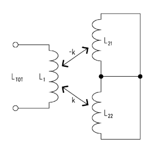
FIGURE 7 is a schematic of the variable integrated inductor shown in FIGURE 6
in which a primary inductor is electromagnetically coupled to a pair of
secondary
inductors and the secondary inductors are connected in series in accordance
with the present invention;
FIGURE 8 is a schematic of the variable integrated inductor shown in FIGURE 6
in which the primary inductor is electromagnetically coupled to a pair of
CA 02620623 2008-02-18
WO 2007/025875
PCT/EP2006/065437
6
secondary inductors and the secondary inductors are connected in parallel in
accordance with the present invention;
FIGURE 9 is a diagram that illustrates a single-turn figure 8 shaped primary
inductor which can be used along with secondary inductors (not shown) to make
the variable integrated inductor in accordance with the present invention;
FIGURE 10 is a block diagram of an exemplary variable integrated inductor
which has a single-turn figure 8 shaped primary inductor that is
electromagnetically coupled to two secondary inductors which are connected to
one another in series in accordance with the present invention;
FIGURE 11 is a block diagram of an exemplary variable integrated inductor
which has a single-turn figure 8 shaped primary inductor that is
electromagnetically coupled to two secondary inductors which are connected to
one another in parallel in accordance with the present invention;
FIGURE 12 is a block diagram of an exemplary variable integrated inductor that
has a double-turn figure 8 shaped primary inductor that is electromagnetically
coupled to two secondary inductors in accordance with the present invention;
FIGURE 13 is a block diagram of an exemplary variable integrated inductor that
has a cloverleaf shaped primary inductor that is electromagnetically coupled
to
four secondary inductors in accordance with the present invention;
FIGURE 14 is a block diagram that illustrates the basic components of a multi-
band radio transceiver which incorporates two variable integrated inductors
like
the ones shown in FIGURES 6-12 in accordance with the present invention; and
FIGURE 15 is a flowchart illustrating the basic steps of a method for
manufacturing the variable integrated inductor in accordance with the present
invention.
DETAILED DESCRIPTION OF THE DRAWINGS
Referring to FIGURE 6, there is a block diagram illustrating a VCO 600 that
has a
LC resonator circuit 602 which includes a variable integrated inductor 604
CA 02620623 2008-02-18
WO 2007/025875
PCT/EP2006/065437
7
(present invention) and a variable capacitor 606. The variable integrated
inductor 604 implements a unique inductive switching technique which is
described below that enables it's inductance to be switched between two or
more
values. As a result, the VCO 600 that uses both the variable integrated
inductor
604 and the variable capacitor 606 has a tuning range which can be extended by
utilizing both inductive switching and capacitive switching (see Equation No.
1).
In the past, this extended tuning range was not possible, because the
traditional
VCO 114 (for example) had a tuning range that could be changed by using only
capacitive switching (via the variable capacitor 123) since the inductor 121
was
fixed (see FIGURE 1).
The variable integrated inductor 604 implements this unique inductive
switching
technique by adding a number of secondary inductors in the same chip area as a
primary inductor (see FIGURES 10-13). The secondary inductors are not
physically connected to the primary inductor but instead are
electromagnetically
coupled to the primary inductor. And, the secondary inductors themselves can
be connected to one another in different configurations/topologies so one can
change the influence that the secondary inductors have on the primary
inductor.
In particular, one can switch the configuration/topology of the secondary
inductors and change a value of the total inductance that is output by the
primary
inductor.
It is not a simple task to add new components like the secondary inductors to
an
inductor because those new components introduce new parasitic elements that
can degrade the quality factor of the inductor. To avoid this problem, the
preferred embodiment of the present invention uses two secondary inductors L21
and L22 that are electromagnetically coupled and not physically coupled to a
primary inductor L1 (see FIGURES 7-8). The two secondary inductors L21 and
L22 should have identical inductances and they should have identical couplings
to
the primary inductor L1. In addition, the two secondary inductors L21 and L22
should have coupling coefficients k with opposite signs. In this way, the
resulting
CA 02620623 2008-02-18
WO 2007/025875
PCT/EP2006/065437
8
equivalent inductance of the three electromagnetically coupled structures L1,
L21
and L22 depends on how the two secondary devices L21 and L22 are connected to
each other.
If the two secondary inductors L21 and L22 are connected in series as depicted
in
FIGURE 7, then the effects of the two secondary inductors L21 and L22 cancel
each other out due to the opposite signs of the coupling coefficients k and -
k. In
this case, no current will flow on the side which has the two secondary
inductors
L21 and L22 and the inductance and 0-factor of the primary inductor L1 will
remain
unaffected as indicated by the following equation:
LTOT = L1 Equation No. 2
However, when the two secondary inductors L21 and L22 are connected in
parallel
as depicted in FIGURE 8, then there is no longer a cancellation effect. The
resulting inductance value of the primary inductor L1 will decrease to a new
value
LTOT that depends on the magnitude of the coupling coefficient k as indicated
in
the following equation:
LTOT = LA1-2=k2) Equation No. 3
In this topology, the overall 0-factor of the variable integrated inductor 604
will
also decrease due to the fact that the loss resistance is not reduced by the
same
amount as the inductance value. As can be seen in FIGURES 7 and 8, the two
secondary inductors L21 and L22 are always connected to one another to form a
closed circuit it is the only topology within this closed circuit that can be
changed
by connecting them in series or parallel.
In the preferred embodiment, the integrated inductors L1, L21 and L22 are
implemented as metal traces on top of a semiconductor substrate (chip). All of
CA 02620623 2008-02-18
WO 2007/025875
PCT/EP2006/065437
9
the important performance parameters like the inductance value, the 0-factor,
and the electromagnetic coupling to other metal structures are defined by the
geometric properties of the inductor layout together with the material
properties
of the substrate. As such, it is important to properly size and layout the
metal
traces which are used to make the integrated inductors L1, L21 and L22. A
description is provided next about some different layouts which can be used to
make the integrated inductors L1, L21 and L22.
Referring to FIGURE 9, there is illustrated a block diagram that shows a
layout of
a single-turn figure 8 shaped primary inductor L1. In this example, the
primary
inductor L1 has the form of a single-turn figure 8 shaped structure with an
upper
loop 902 and a lower loop 904. By virtue of the figure 8 shape, current in the
upper loop 902 travels in a direction (e.g., clockwise, see arrows) that is
opposite
to current in the lower loop 904 (e.g., counterclockwise, see arrows). As a
result,
the figure-8 geometry has the advantage that the magnetic fields 906 and 908
emitted from the two sub-loops 902 and 904 have opposite directions. And, this
means that the magnetic fields 906 and 908 which emanate at a certain distance
from the primary inductor L1 tend to counteract each other so as to reduce the
far
field effect that the primary inductor L1 can have on other components (for
more
details about this advantage see co-pending U.S. Patent Application Serial No.
10,919,130). Another advantage of this symmetrical layout for the primary
inductor L1 is that it is well suited for implementing the inductive switching
technique of the present invention as discussed next.
Referring to FIGURE 10, there is illustrated a block diagram of an exemplary
variable integrated inductor 604 that shows two secondary inductors L21 and
L22
that are electromagnetically coupled to the single-turn figure 8 shaped
primary
inductor L1 in accordance with the present invention. A switch 1002 in the
center
is left open resulting in a closed circuit series connection of the two
secondary
inductors L21 and L22. For instance, the switch 1002 can be a large metal
oxide
semiconductor (MOS) transistor 1002 that can be controlled by software. The
CA 02620623 2008-02-18
WO 2007/025875
PCT/EP2006/065437
full layout symmetry between the inductors L1, L21 and L22 guarantees that the
coupling coefficients k of the second inductors L21 and L22 are identical in
magnitude. And, the symmetrical figure-8 shape of the primary inductor L1
automatically ensures that the coupling coefficients k of the secondary
inductors
5 L21 and L22 have opposite signs. This is due to the fact that the primary
inductor
L1 has two sub-loops 902 and 904 which have opposing magnetic fields 906 and
908. As a result, the variable integrated inductor 604 in this configuration
functions like the circuit shown in FIGURE 7 and the total inductance LT0T is
equal to the inductance of the primary inductor L1.
10 Referring to FIGURE 11, there is illustrated a block diagram of the
exemplary
variable integrated inductor 604 shown in FIGURE 10 where the switch 1002 is
closed so the secondary inductors L21 and L22 are connected in parallel.
Again,
the full layout symmetry between the inductors L1, L21 and L22 guarantees that
the coupling coefficients k of the second inductors L21 and L22 are identical
in
magnitude. And, the geometries of the inductors L1, L21 and L22 have not
changed so the secondary inductors L21 and L22 still have coupling
coefficients k
with opposite signs. As a result, the variable integrated inductor 604 in this
configuration functions like the circuit shown in FIGURE 8 and the total
inductance LTOT is reduced in accordance with Equation No. 3.
Referring to FIGURE 12, there is illustrated a block diagram of an exemplary
variable integrated inductor 604' that has two secondary inductors L21 and L22
which are electromagnetically coupled to the double-turn figure 8 shaped
primary
inductor L1 in accordance with another embodiment of the present invention.
The double-turn figure 8 shaped primary inductor L1 is very similar to the
single-
turn figure 8 shaped primary inductor L1 shown in FIGURES 10-11 in that it has
an upper loop 902 and a lower loop 904. However, the double-turn figure 8
shaped primary inductor L1 that has 2 turns has a lower 0-factor and is
structurally smaller for the same inductance value when compared to the single-
turn figure 8 shaped primary inductor L1 shown in FIGURES 10-11. The
CA 02620623 2008-02-18
WO 2007/025875
PCT/EP2006/065437
11
switching mechanism 1002 can be the same as the one shown in FIGURES 10-
11.
In both embodiments of the variable integrated inductor 604 and 604', it
should
be noted that depending on the actual layout of the inductors L1, L21 and L22,
the
inductance values of the connected secondary inductors L21 and 1_22 might
differ
slightly between the series configuration and the parallel configuration.
However,
this is not a problem provided that the inductance values are equal L21 = L22
between the two secondary inductors L21, L22 themselves.
Although one pair of secondary inductors L21 and L22 is shown and described
above with respect to FIGURES 7-12, it is also possible to implement several
pairs of secondary inductors which enables the primary inductor L1 to output
more than two inductance values. The use of multiple pairs of secondary
inductors may be desirable since using inductive switches instead of
capacitive
switches for frequency tuning is probably less sensitive to differences in
process
parameters. This is because the inductive switches are closely linked to
device
geometry which can be more tightly controlled. For instance, the magnitude of
the coupling coefficients k can be controlled by using laser-cutting tools to
change the geometry (e.g., size, shape) of the secondary inductors relative to
the
primary inductor L1. The laser-cutting tools can also be used to replace the
MOS
switch 1002 if one wants to perform a once for all tuning (trimming) of the
variable integrated inductor 604 during production to compensate for process
variations in other components that influence the VCO frequency.
A large variety of geometries can be utilized for switched variable integrated
inductors 604 which implement multiple pairs of secondary inductors provided
that they can in a simple way support opposite signs for the various coupling
coefficients k of the secondary inductors. One such example is shown in
FIGURE 13, this variable integrated inductor 604" has a cloverleaf shaped
primary inductor L1 and four secondary inductors L21, L22, L23 and L24. The
four
secondary inductors L21, L22, L23, and L24 are used for inductance switching
CA 02620623 2008-02-18
WO 2007/025875
PCT/EP2006/065437
12
where two of the secondary inductors L21 and L23 (for example) have positive
coupling coefficients k and the other two secondary inductors L22 and L24 (for
example) have negative coupling coefficients -k. The switching mechanism 1002
can be the same as the one shown in FIGURES 10-11.
As indicated above, the variable integrated inductors 604, 604' and 604" can
be
implemented in a wide variety of devices. For example, devices like tuned
amplifier loads, impedance matching networks, a digitally controlled
oscillator or
other types of frequency selective LC-networks can benefit from incorporating
and using the extended tuning range of the variable integrated inductors 604,
604' and 604". In addition, a multi-band radio transceiver 1400 like the one
shown in FIGURE 14 can benefit from the use of two variable integrated
inductors 604, 604' and 604".
Referring to FIGURE 14, there is a block diagram illustrating the basic
components of the multi-band radio transceiver 1400 in accordance with the
present invention. The multi-band radio transceiver 1400 (e.g., wireless
communication device 1400) shown includes an antenna 1402, a
transmit/receive (T/R) unit 1404, a receive path 1406, a transmit path 1408
and a
base-band signal processing unit 1410. The receive path 1406 includes a mixer
1412 that is used together with a VCO 1414 to down-convert a RF frequency
signal, which is received by the antenna 1402, to a lower frequency that is
suitable for further signal processing in the base-band signal processing unit
1410. The transmit path 1408 includes a mixer 1416 that is used together with
a
VCO 1418 to up-convert a base-band signal, which is received from the base-
band signal processing unit 1410, to a higher frequency before it is
transmitted
by the antenna 1402.
The multi-band radio transceiver 1400 has the same configuration as the
traditional multi-band radio transceiver 100 shown in FIGURE 1 except that the
tuning ranges of the VCOs 1414 and 1418 are larger than the tuning ranges of
the VCOs 114 and 118 used in the traditional multi-band radio transceiver 100.
CA 02620623 2008-02-18
WO 2007/025875
PCT/EP2006/065437
13
Again, the VCOs 1414 and 1418 have an extended tuning range because they
can use a combination of both inductive switching (via the variable integrated
inductor 604, 604' and 604") and capacitive switching (via the variable
capacitor
606). In the past, this extended tuning range was not possible because the
traditional VCOs 114 and 118 had a tuning range that could be changed by using
only capacitive switching (via the variable capacitor 123) since the inductor
121
was fixed (see FIGURE 1). For clarity, the description provided herein about
the
multi-band radio transceiver 1400 omits certain details about well known
components that are not necessary to understand the present invention.
Another advantage associated with using the variable integrated inductors 604,
604' and 604" in the multi-band radio transceiver 1400 (or any device) is that
there is less mutual EM coupling between the VCOs 1414 and 1418. This is
because, each variable integrated inductor 604, 604' and 604" is symmetrical.
And, since each variable integrated inductor 604, 604' and 604" consists of
symmetrical multiple loops this means that each of them emit magnetic fields
that
tend to counteract themselves. As a consequence, two variable integrated
inductors 604, 604' and 604" can be placed near each other and oriented in a
way such that the induced current in one variable integrated inductor 604,
604'
and 604" due to the magnetic field originating from the other variable
integrated
inductor 604, 604' and 604" is significantly reduced. For a more detailed
discussion about this advantage and other advantages associated with using a
symmetrical primary inductor, reference is made to the co-pending U.S. Patent
Application Serial No. 10/919,130.
Referring to FIGURE 15, there is a flowchart that illustrates the basic steps
of a
method 1500 for manufacturing the variable integrated inductor 604, 604' and
604" in accordance with the present invention. Beginning at step 1502, a multi-
loop primary inductor L1 is formed by placing metal traces on a chip. At step
1504, one or more pairs of secondary inductors L21 and L22 (for example) are
formed by placing metal traces on the chip. As discussed above, the secondary
CA 02620623 2008-02-18
WO 2007/025875
PCT/EP2006/065437
14
inductors L21 and L22 are electromagnetically coupled to the multi-loop
primary
inductor L1. And, the secondary inductors L21 and L22 form a closed circuit
which
has a changeable topology that can be switched between a series connection
and a parallel connection. At step 1506, a switch 1002 is formed on the chip.
The switch 1002 is used to alter the changeable topology of the secondary
inductors L21 and L22 and change an inductance value which is output by the
multi-loop primary inductor L1.
Following are some additional features and advantages associated with the
present invention:
* Using a switchable integrated inductor in the VCO resonator extends the
frequency tuning range beyond the limit imposed by capacitive switches. This
makes it possible to use a single VCO to cover more bands in a multi-band
radio
transceiver. Also, the chip area of an integrated VCO is already relatively
large
due to the inductor itself and a reduced number of VCOs means a substantial
cost reduction for the transceiver chip.
* The switchable integrated inductor has a inductance value that can be set
to an
arbitrary value (within certain limits) by changing the coupling coefficient K
between the windings. The step is almost independent of process variations
since it is determined mainly by geometrical parameters.
* The secondary inductors are not galvanicly connected to the resonator
circuit.
This minimizes the parasitic effects and makes it easier to implement the
switch
element since one can apply the most suitable voltage to the secondary
windings.
* The inductive switching technique can be used for a large variety of
inductor
layouts and it's use will not take up much more chip area than is used by a
traditional inductor.
* The inductive switching technique can be applied so the inductor layouts
will
have reduced electromagnetic coupling to other conductors that are on-chip or
off-chip.
CA 02620623 2014-02-17
The secondary inductors can introduce additional losses when they are in
parallel connection in the low inductance state. And, as a consequence, the
quality-factor of the inductor can drop and the phase noise performance of
the VCO can be reduced. However, this can easily be compensated for by
5 increased supply current in applications where the phase noise
requirements
are stringent.
In the event, that variations in the manufacturing process result in a VCO
(which contains the variable integrated inductor) that has an oscillation
frequency which is too low, then a production trimming of the inductors can
10 be performed to increase the oscillation frequency to an acceptable
value.
Although several embodiments of the present invention have been illustrated
in the accompanying Drawings and described in the foregoing Detailed
Description, it should be understood that the embodiments disclosed are
capable of numerous rearrangements, modifications and substitutions
15 without departing from the scope of the invention, which is defined
solely by
the claims appended hereto.