Note: Descriptions are shown in the official language in which they were submitted.
CA 02621213 2008-03-10
AUDIO MESSAGE TRANSFER SHEET AND
MANUFACTURING METHOD THEREOF, AND POWER SUPPLY CIRCUIT
REFERENCE TO RELATED APPLICATION
This application is a division of copending Canadian Patent Application
No. 2,536,700 filed August 30, 2004.
BACKGROUND OF THE INVENTION
1. Field of the Invention
The present invention relates to an audio message transfer sheet wRh
built-in audio information recording/reproducing means capable of
recording/reproducing audio information and a manufacturing method thereof,
an audio information output sheet, a POP (Point of Purchase) indicator, a
sound information delivery apparatus, an audio information delivery
component, a label, and a power supply circuit used for the same and a
manufacturing method thereof.
2. Description of the Related Art
Conventionally, with regard to an article to be delivered such .as direct
mail or greeting card, a sender creates the article, specifies the destination
of
the article and then delivers the created article to the specified
destination. The
article created and delivered in this way may be made up of a-printed matter
describing information of which the sender wants to notify the
destination enclosed in an envelope or information of which the sender wants
to notify the destination printed on a sheet such as post card, etc.
At the destination of the article delivered, after reception of the articde,
the information printed on the article is browsed and in this way the
information of which the sender wants to notify the destination is recognized.
However, when the article to be delivered with printed information of
which the sender wants to notify the destination is sent by the sender, the
information printed on the article delivered from the sender is browsed at the
CA 02621213 2008-03-10
destination, and thereby the information of which the sender warAs to notify
the destination is transferred to the destination, a desired message of the
sender of the article to be delivered can be transferred to the destination
only
visually and in this way the type of transferable information is limited.
Therefore, an information carrier constructed so as to incorporate an
audio apparatus capable of recording/reproducing audio information in direct
mail and transfer the message with audio is conceived.
Fig. 1 a is a plan view of an information carrier with an audio apparatus
capable of recording/reproducing audio information incorporated in direct
mail, Fig. 1 b is a cross-sectional view along the line A-A' shown in Fig. 1
a.
As shown in Fig. 1 a, 1 b, this conventional example is constructed of a
direct mail component 501 a having a display section 502 on which address
information, etc., is printed with a built-in audio apparatus 503 capable of
recording/reproducing audio information. Furthermore, this audio apparatus
503 is constructed of a PC board 507 mounted with an IC memory 512 for
recording audio information and a power supply battery 511, a speaker 509
which outputs audio information recorded in the IC memory 512, a switch 508
to be operated when outputting the audio information recorded in the iC
memory 512 from the speaker 509, all of which are mounted on a mount
503a, and pasted to the direct mail component 501 a, covered with a cover
513 having a hole from which the switch 508 and speaker 509 are exposed.
In the direct mail 501 constructed as shown above, address
information, etc., is printed on the display section 502 and audio information
is recorded in the audio apparatus 503, and then the audio apparatus 503
with audio in which information is recorded is pasted to the direct mail
component 501 a and delivered to the destination. At the destination of the
2
CA 02621213 2008-03-10
direct mail 501, after reception of the direct mail 501 if the switch 508 is
operated, the audio information recorded in the audio appa-ratus 503 is output
through the speaker 509. This direct mail 501 is disclosed in Japanese
Patent Application Publication No. 1999-70770.
However, since the information carrier incorporating the above
described audio apparatus is constructed of an audio apparatus mounted on
or pasted to the direct mail component on which address information, etc., is
printed, there is a problem that the area to which the audio apparatus is
pasted becomes so thick that the address information, etc., cannot be printed
with the audio apparatus incorporated. For this reason, in the case of the
above described information carrier, the address information, etc., is printed
on the direct mail component first and then the audio apparatus is mounted
on or pasted to the direct mail component.
Furthermore, since the audio apparatus is mounted on or pasted to
the direct mail component and the area is thick, if the direct mail is folded
or
an external force is applied to this area, the audio apparatus may be peeled
from the direct mail component. When the direct mail is two-folded or folded
in a Z-figure, the direct mail should be folded in such a way as to avoid the
area where the audio apparatus is mounted, which causes a problem that the
area where the audio apparatus is mounted or the area which becomes a
folding line when the direct mail is folded is limited.
Furthermore, the above described audio information output sheet
capable of recording/reproducing audio information needs to be provided with
audio information outputting means such as a speaker for outputting the
recorded audio information, but the audio information outputting means such
as a speaker is required to have certain dimensions to secure a
CA 02621213 2008-03-10
predetermined sound volume, which results in a problem that it is diff~cul# to
reduce the size of the entire audio information output sheet.
Furthermore, POP indicators on which advertisement information on
goods, etc., is displayed as a POP are conventionally attached to showcases
at a shop such as a department store, supermarket or recently a
convenience store, and sales promotion activities for goods, etc., are
conducted using these POP indicators. For such POP indicators, various
display methods or various shapes of POP indicators are considered in order,
to attract attention of visitors to the store.
For example, Japanese Patent Application Publication No. 2001-
178599 discloses a POP indicator with a window through which inventory
tags attached together with the POP indicator are visible formed in a
showcase and a noticeably decorated window frame formed integral with the
POP display section to thereby attract attention to advertisement information
displayed on the POP display section.
However, in a conventional POP indicator, only advertisement
information on goods is displayed as a POP, and therefore visitors to the
store can only visually recognize advertisement information and there are
cases where depending on the design of the POP or size of characters, etc.,
such a POP indicator may not be adequate to attract attention.
Furthermore, in the case of the POP indicator, an amount of
information of advertisement information displayed as a POP is limi#ed by the
size thereof and the POP indicator is often attached to a showcase and in
that case, the size of the POP indicator is preferably not too large so that
it is
kept out of the way of a visitor when the visitor picks up a product from the
showcase, and therefore there is a problem that it is difficult to display a
large
4
CA 02621213 2008-03-10
amount of advertisement information as a POP.
Furthermore, there are a variety of types of devices capable of
recording/reproducing sound information such as audio. With the slimming
down of batteries, downsizing of recording control elements, slimming down
of pronouncing devices, etc., in recent years, there is a proposal on a thin
audio recording/reproducing instrument combining these elements. As a
product which uses this audio recording/reproducing instrument, for example,
a mail card which incorporates a thin recording/reproducing instrument in one
sheet of a double-page sheet, designed to output audio from the
recording/reproducing instrument through a switch operation linked with an
operation of opening the other sheet is disclosed in Japanese Patent
Application Publication No. 1997-202072. Furthermore, a duplicate delivery
slip which combines a recording/reproducing instrument which records audio
information directed to the destination of an article to be delivered with a
slip
is also disclosed in Japanese Patent Application Publication No. 2003-
246165.
Now, the above described delivery slip provided with a
recording/reproducing instrument is only designed so that the sender of the
article inputs audio and the receiver reproduces the audio, and therefore it
does not cause much time and trouble when the sender transmits a message
with audio to the receiver and can be useful because in this way it is
possible
to make an impression to the receiver that the article is a present given with
heartfelt feelings.
___ __ Howev.er, suc_h_ a recording/reproducing instrument can be used only
when sending an article to be delivered and there has been actually no
recording/reproducing instrument that can be used to send a message with
5
CA 02621213 2008-03-10
audio itself as a main article to be delivered. Therefore, there has been a
demand for one which is thin, without being bulky, capable of delivering a
message with audio using recording/reproducing means with excellent
usability during recording or reproduction.
Furthermore, Japanese Examined Application Publication No. 1991-
1 45433 and Specification of Japanese Patent No. 2889151 disclose an audio
card capable of recording/reproducing audio information.
Such an audio card is provided with audio inputting means for
inputting audio information, recording means for recording audio information
input through audio inputting means, audio outputting means for outputting
the audio information recorded in the recording means, a recording button
which is pressed when audio information is input through the audio inputting
means, a playback button which is pressed when audio information is output
through the audio outputting means and controlling means for controlling
these operations, and designed so that the audio information is recorded by
pressing the recording button and the audio information is reproduced by
pressing the playback button.
Here, the audio information is recorded in the audio card capable of
recording audio information in such a way as to overwrite audio information
recorded in the recording means with the audio information input through the
audio inputting means. For this reason, after audio information is recorded
in the recording means, if the recording button is pressed mistakenly, the
audio information already recorded in the recording means is erased.
Therefore, above described Japanese Examined Application Publication No.
1991-45433 describes a technology which adopts a structure that the
recording button is easily detachable so that the recording button is detached
6
CA 02621213 2008-03-10
after audio information is recorded, thereby avoid" audio information from
being erased by misoperation of the recording button. Furthermore, the
audio card described in the above described Specification of Japanese
Patent No. 2889151 is constructed in such a way that when the playback
button and recording button are simultaneously pressed after audio
information is recorded, control is performed such that further recording of
audio information is prohibited, thereby avoiding audio information from being
erased by misoperation of the recording button.
However, as described above, in the case of t~he stn.icture that the
recording button is made easily detachable so that the recording button is
detached after audio information is recorded to thereby avoid audio
information from being erased by misoperation of the recording button, when
an audio card with audio information -recorded therein is delivered, the audio
card is delivered to the destination with part of the audio card detached,
causing a problem that the appearance of the audio card to be delivered
becomes unattractive.
Furthermore, in the case of the structure that when the playback
button and recording button are pressed simultaneously after audio
information is recorded, further recording of audio information is prohibited,
there is a problem that it is not possible to visually confirm whether the
recording of audio information is prohibited or not. For this reason, there
may be a case where although the recording is not prohibited yet after audio
information is recorded, the user may send the audio card without placing the
audio card in a prohibited _state_believing that the recording is already
prohibited. In that case, the recording button may be pressed mistakenly
later and the audio information recorded may be erased. Furthermore, in
7
CA 02621213 2008-03-10
order to prohibit the recording of audio information, the recording button is
pressed to record the audio information, and therefore when the recording
button is pressed before the -playback button is pressed, part of the audio
information recorded may be erased.
Furthermore, a double postal card combining a transmitting message
card and reply message card is conventionally used for many applications
such as invitation for an event, for example, another party of a wedding
ceremony, an order form of goods or service, etc. Address information such
as the address, name of the receiver is written on the front of such a
transmitting message card and information transmitted from the sender to the
receiver is written on the back. Furthermore, address information such as
the address, name of the sender is written on the front of the reply message
card and an area is provided on the back thereof for entering information to
be transmitted from the sender to the receiver.
The double postal card structured in this manner is folded along a
connecting area between the transmitting message card and reply message
card in such a way that address information such as the address, name of
the receiver is exposed and sent to the destination, and at the destination
the
transmitting message card is cut from the reply message card along the
connecting area, the information to be transmitted from the receiver to the
sender is written on the back of the reply message card and only the reply
message card is sent back to the sender.
As such, the double postal card combining the transmitting message
card and reply message card has a limited amount of information that can be
transferred from the sender to the receiver or from the receiver to the sender
and both the transmitting message card and reply message card need to
8
CA 02621213 2008-03-10
include the address information, which further limi#s the amount of
information thereof.
Therefore, Japanese Patent Application Publication No. 2001-121858
discloses a double postal card having a structure that a sheet having a
vertical size equal to or double the standard vertical size of a postal card
and
a horizontal size four times the standard horizontal size is foided into the
size
of the postal card, so that a greater amount of information can be
#ransferr.ed
in the standard size of the postal card.
However, though an amount of information that can be transferred
may be increased with such a double postal card, the information can be
transferred from the sender to the receiver or from the receiver to the sender
only visually, which limits the type of information that can be transferr,ed.
Here, if the audio card disclosed in above described Japanese
Examined Application Publication No. 1991-45433 is applied to the above
described double postal card, information can be transferred with audio from
the sender to the receiver or from the receiver to the sender of the doubie
postal card. For example, in the case of an invitation to another partyof a
wedding ceremony, if a reply messag.e card is structured so as to be able to
record audio information and a reply about whether or not 4o attend the other
party of the wedding ceremony is sent from the receiver of the invitation with
a message recorded in the reply message card to the sender of the invitation,
the sender of the invitation can receive the message with audio from the
receiver of the invitation.
However, even with the above described double postal card with the
structure that the recording button is easily detachable so that detaching the
recording button after audio information is recorded prevents audio
9
CA 02621213 2008-03-10
information from being erased by misoperation of the recording button, when
this reply message card is sent with audio information recorded in the reply
message card as described above, the reply message card is sent back to
the sender with part thereof detached, which results in a problem that the
appearance of the reply message card sent back becomes unattractive.
Such a problem is not limited to the above described double postal
card, and can also occur with an audio information delivery component
combining a transmitting message section and reply message section.
Furthermore, a label structured so that it can be pasted to an object to
be labeled such as an article using an adhesive is conventionally provided in
various modes according to the use and used for various applications. Such
a label can transfer information with the information printed or written on
the
surface thereof.
Furthermore, in recent years, Japanese Patent Application Publication
No. 2001-242788 discloses a label with information to be transferred
displayed on the surface thereof and processed into a convex form including
Braille characters, capable of transferring information to the visually
handicapped, too. In this way, displaying information to be transferred on
the surface of a label and processing it into a convex form including Braille
characters allows the information displayed on the surface to be transferred
to the able-bodied and allows the information expressed through convex form
processing to be transferred to the visually handicapped, too.
However, the above described label, to the surface of which convex
form processing including Braille characters is applied, can transfer
information expressed in Braille characters to the visually handicapped who
can read Braille characters, but cannot transfer information to the visually
CA 02621213 2008-03-10
handicapped who cannot read Braille characters.
Here, those who can read Braille characters account for less than
20% of all the visually handicapped and the proportion is less than 5% when
people with weak sight and senior citizens are included. For this reason,
even if a label, to the surface of which convex form processing including
Braille characters is applied is used, there still is a problem that it is
difficult to
transfer information to many visually handicapped and people with weak
sight.
Furthermore, in recent years, not a small number of products driven
by battery power are required to save space of a power supply section in
order to achieve the downsizing and multi-functions and as a means for
meeting such a demand, a button-type bat#ery is used. Furthermore, the
above described audio card, etc., requires a low-profile battery.
Here, in recent years, Japanese Patent Application Laid-Open No.
2000-502206 discloses a paper battery having a structure of a positive
electrode and negative electrode laminated together through an electrolytic
layer. This paper battery is partitioned by the electrolytic layer into the
positive electrode and negative electrode and the respective electrodes of
the positive electrode and negative electrode are exposed on different
surfaces of the paper battery. For this reason, when such a paper battery is
mounted on a circuit substrate to construct a power supply circuit, one of the
positive electrode and negative electrode does noi face the circuit substrate
and the electrode not facing the circuit substrate will have a connection
terminal for providina a connection with the circuit substrate connected by
soldering, etc. through which it is connected to the circuit substrate.
However, when the electrodes of the paper battery are connected to the
11
CA 02621213 2008-03-10
circuit substrate through the connection terminal, the resistance between the
electrode and the circuit substrate increases. Moreover, doing so requifes
an additional operation, which results in reduced productivity and increased
cost.
Therefore, the Specification of Japanese Patent No. 2866383
discloses a technology of folding part of a paper battery so that a positive
electrode and a negative electrode are formed on the same surface. This
technology folds part of the paper battery whose positive electrode and
negative electrode are formed on different surfaces, superimposes this paper
battery on the circuit substrate through an insulating film provided with
holes
through which parts of the positive electrode and negative electrode are
exposed and connects the positive electrode and negative electrode of the
paper battery, and circuit substrate through these holes.
However, as described above, when part of the paper battery is folded
and the positive electrode and negative electrode are thereby formed on the
same surface, this means that the paper battery is continuously used with
part of the paper battery folded and this involves a problem that the paper
battery is used in an environment unfavorable to the paper battery compared
to the use of the paper battery without folding.
Furthermore, as described above, in the case of a power supply circuit
made up of a paper battery laminated on the circuit substrate, it is possible
to
apply, for example, an anisotropic/conductive film or an
anisotropic/conductive adhesive to a connection terminal of the paper battery,
and then mount the paper battery on the circuit substrate and eaectrically
connect and bond together the paper battery and circuit substrate using the
anisotropic/conductive film or anisotropic/conductive adhesive.
12
CA 02621213 2008-03-10
However, as described above, when the paper battery and -circuit
substrate are connected using an anisotropic/conductive film or
anisotropic/conductive adhesive and the paper battery is mounted on a circuit
substrate to thereby manufacture a power supply circuit, the
anisotropic/conductive film or anisotropic/conductive adhesive is applied to
the electrodes of the paper battery first, and then the paper battery and
circuit
substrate are provisionally crimped and then the paper battery and circuit
substrate are completely crimped, which results in a problem that such a
manufacturing step is more complicated and productivity is reduced.
Furthermore, there is also a problem that the anisotropic/conductive
film or anisotropic/conductive adhesive cannot be easily controlled, is
expensive and thereby requires complicated control and increases the
manufacture cost of the power supply circuit.
SUMMARY OF THE INVENTION
It is an object of the present invention to provide a bendable or
foldable audio message transfer sheet allowing information to be printed
thereon and a manufacturing method thereof.
Furthermore, it is another object of the present invention to provide an
audio information output sheet which can be downsized while securing a
predetermined sound volume.
Furthermore, it is a further object of the present invention to provide a
POP indicator which can attract sufficient at#ention of consumers and contain
a large amount of_adveriisement information.
Furthermore, it is a challenge of the present invention to allow the
above described recording/reproducing means to be delivered on a delivery
13
CA 02621213 2008-03-10
system based on a conventional delivery slip and it is a still further object
of
the present invention to facilitate delivery of a voice message as a present.
Furthermore, it is a still further object of the present invention to
provide an audio message transfer sheet whose appea-rance does not
become unattractive when recording of audio information is prohibited and
which makes it possible to visually confirm that recording is prohibited.
Furthermore, it is a still further object of the present invention to
provide an audio information delivery component comprising a transmitting
message section and a reply message section connected together, wherein
the reply message section is structured so as to be able to record audio
information and it is possible to prevent recorded audio information from
being erased mistakenly without degrading the appearance.
Furthermore, it is a still further object of the present invention to
provide a label capable of transmitting information to the able-bodied and the
visually handicapped alike.
Furthermore, it is a still further object of the present invention to
provide a power supply circuit comprising a paper battery whose -positive
electrode and negative electrode are exposed on different surfaces, mounted
on a sheet-like circuit substrate, the power supply circuit capable of being
formed without increasing the resistance between the paper battery and
circuit substrate and without folding the paper battery.
Furthermore, it is a still further object of the present invention to
provide a method of manufacturing a power supply circuit comprising a paper
_battery connected to a circuit substrate, capable of improving productivity
without increasing the manufacturing cost.
In the present invention, audio information recording/reproducing
14
CA 02621213 2008-03-10
means capable of recording/reproducing audio information has a sheet-like
structure, and this audio information recording/reproducing means is
sandwiched between two support sheets and these suppoft sheets are
further sandwiched between two surface sheets, which allows the audio
information recording/reproducing means to be bent or folded, and the audio
information recording/reproducing means is sandwiched from front and back
in only part of the area of the two support sheets facing the audio
information
recording/reproducing means, and therefore the difference in thickness
between the area in which the audio information recording/reproducing
means is incorporated and other area is reduced though the audio
information recording/reproducing means is incorporated therein, which
allows information to be printed on the surface sheet.
Furthermore, making the outside shape of the two support sheets
equal to the outside shape of the surface sheets can make the thickness of
the entire audio message transfer sheet substantially uniform.
Furthermore, dividing each of the two support sheets into a plurality of
portions makes it possible to increase the degree of freedom in bending and
folding of the audio message transfer sheet.
Furthermore, adopting a structure that the two support sheets are
connected along a bend line facilitates positioning of the two support sheets.
Furthermore, when audio information outputting means provided for
the audio information recording/reproducing means for outputting audio
information is constructed of a piezo-electric element which outputs audio
information, a fi.l.m_sheet having a targer diameter than the piezo-electric
element, pasted to one surface of the piezo-electric element and a
diaphragm provided with a hole having a diameter larger than the diameter of
CA 02621213 2008-03-10
the piezo-electric element and smaller than the diameter of the film sheet,
pasted to a film sheet in such a way that the piezo-electric element fAs into
the hole, and the diaphragm is bonded to the support sheet only in the area
of the surface of bonding with the film sheet which is not bonded to the film
sheet, it is possible to prevent the thickness of the area where the audio
information outputting means is provided from increasing and cause the
audio information outputting means to be fixed to the surface sheet without
being bonded thereto and thereby avoid vibration of the piezo-electric
element and diaphragm from being interfered.
Furthermore, by adopting a structure that two support sheets
sandwich the audio information recording/reproducing means around
operating means and the audio information recording/reproducing means is
mounted on one support sheet in the area in which the operating means is
provided and making the height of the operating means lower than the
thickness of the support sheet, the operating means is surrounded by the
support sheet which is thicker than the height of the operating means and it
is
thereby possible to prevent the operating means from being operated when
force majeure is applied from outside.
Furthermore, if an ink receiving layer is laminated on the surface of at
least one of the two surface sheets which does not face the support sheet,
when information is printed on the surface sheet by an ink-jet printer later,
the
information is printed clearly on the surface sheet.
Furthermore, if this ink receiving layer is superimposed on the surface
--slaeet before the support sheets sandwiching the audio information
recording/reproducing means are sandwiched between the surface sheets, it
is possible to laminate the ink receiving layer with excellent flatness of the
16
CA 02621213 2008-03-10
surface sheets and when the surface sheets consist of single pieces cut out
from a continuous sheet, the ink receiving layer is laminated on the
continuous surface sheet, which facilitates the lamination of the ink
receiving
layer.
Furthermore, according to the present invention, the area of at least
the audio information output section of the audio information
recording/reproducing means sandwiched between the two surface sheets
can be folded along a bend line, and therefore the downsizing can be
achieved by folding the area where at least the audio information output
section is incorporated with respect to other areas without reducing the size
of the audio information output section.
Furthermore, according to the present invention, when mounted on an
object by a mounting member, advertisement information displayed as a
POP on the surface sheet is visually recognized and when the operating
means is operated, audio information recorded in the audio information
recording/reproducing means is reproduced.
In this way, audio information is recorded in the audio information
recording/reproducing means and this audio information is designed to be
reproducible by the operating means, and therefor.e if the advertisement
information is recorded as audio information in the audio information
recording/reproducing means, the advertisement information is visually
recognized and provided as audio information as well, and in this way it is
possible to attract attention of consumers and also include a large amount of
advertisement information.
Furthermore, since this operating means and the surface sheet in the
area where the operating means is pasted protrude from other areas, the
17
CA 02621213 2008-03-10
operating means can be easily operated.
Furthermore, if the surfiace sheet is made of synthetic paper suitable
for printing, it is possible not only to print advertisement information as
aPO1'
on the surface sheet but also to improve the durability of the surface sheet.
In the area where the operating means is pasted in particuiar, the surface
sheet may deteriorate when the operating means is operated, but using
synthetic paper can suppress deterioration of the surface sheet.
Furthermore, when the power supply section which supplies power to
the audio information recording/reproducing means is constructed of a
plurality of paper batteries made up of positive -electrodes and negative
electrodes exposed from different surfaces, if these plurality of paper
batteries are connected in series and the audio substrate which is mounted
with the audio information recording/reproducing means and connecAed to
the power supply section is constructed of a first conductive area connected
to one of both electrodes of the power supply section and a second
conductive area connected to the other of the two electrodes of the power
supply section formed on different surfaces in such a way that both
electrodes of the power supply section are connected to the fifst conductive
area and second conductive area, all that is needed is to connect the
plurality
of paper batteries and the audio substrate only at two locations, which can
reduce the manufacturing cost.
Furthermore, according to the present invention, when a conductive
member is sandwiched between two surface sheets, an IC chip having a
_ storage area and a second__switch are_el_ectrically connected through the
conductive member, and if the second switch is operated in this condition, a
second instruction signal for recording audio information in the IC chip is
18
CA 02621213 2008-03-10
input to the IC chip and the audio information input through the audio
information inputting/outputting means is recorded in the IC chip. Then, if
the conductive member is removed from the two surface sheets, the aC chip
and second switch are electrically left open and even if the second switch is
operated in this condition, the second instruction signal for recording the
audio information in the IC chip is not input to the IC chip and even if audio
information is thereby input via the audio information inputting means, the
audio information is not recorded in the IC chip. For this reason, if the
conductive member is removed from the two surface sheets after the audio
information is recorded in the IC chip, the audio information recorded in the
IC chip is not erased even if the second switch is operated later.
Thus, recording of the audio information in the IC chip is enabled by
the conductive member sandwiched between the two surface sheets and the
recording of the audio information in the IC chip is prohibited by removing
this
conductive member from the two surface sheets, and therefore even if the
recording of the audio information in the IC chip is prohibited, the surface
sheets which become the appearance of the audio message transfer sheet
remain as they are, preventing the appearance from becoming unaftaactivJe.
Furthermore, whether the recording of the audio information in the IC chip is
prohibited or not can be determined through the presence/absence of the
conductive member, and therefore it is possible to visually confirm that the
recording is prohibited.
Furthermore, audio information is recorded in the frrst audio
information recording/reproducing means sandwiched between the two
surface sheets with the transmitting message section and the reply message
section connected. Then, when the transmitting message section is
19
CA 02621213 2008-03-10
separated from the reply message section along the connection part in order
to send the reply message section, wiring for r,ecording audio information
sandwiched between the two surface sheets in such a way as to span the
transmitting message section and the reply message section of the first audio
information recording/reproducing means sandwiched between the two
surface sheets is cut. In this way, when the transmitting message section is
separated from the reply message section, it is not possible to record audio
information in the first audio information recording/reproducing means,
preventing the audio information already recorded in the first audio
information recording/reproducing means from being erased mistakenly.
Furthermore, of the first audio information recording/reproducing means, the
portion other than the wiring for recording the audio information is
sandwiched between the two surface sheets on the reply message section
side, and therefore it is possible for the receiver of the reply message
section
to reproduce the audio information recorded in the first audio information
recording/reproducing means.
Furthermore, according to the present invention, audio information is
recorded in the audio information recording/reproducing means sandwiched
between the two sheet base materials, this label is pasted to an object, the
object is supplied to the destination of the audio information by delivery,
etc.,
and then the audio information recorded in the audio information
recording/reproducing means is reproduced at the destination of the audio
information and the desired audio information is thereby transmitted to the
destination.
Furthermore, according to the present invention, a paper battery is
constructed of a positive electrode and a negative electrode laminated
CA 02621213 2008-03-10
through an electrolytic layer with both the positive and negative eiectrodes
exposed from different surfaces, and the paper bat#ery is connected to a
sheet-like circuit substrate on which a oonductive area to be connected to the
electrodes is formed and a power supply circuit is formed of the paper battery
and the conductive area, in order for one of the positive electrode and
negative electrode to be connected to a first conductive area formed on one
surface of the circuit substrate, the paper battery is mounted on the surface
on which the first conductive area is formed and the other electrode of the
positive electrode and negative electrode is connected to a second
conductive area formed on the other surface, and in this way a power supply
circuit is formed of the paper battery, and the first and second conductive
areas.
In this way, one of the positive electrode and negative electrode
exposed from the different surfaces of the paper battery is connected to the
first conductive area formed on one surface of the sheet-like circuit
substrate,
the other of the positive electrode and negative electrode is conneced to the
second conductive area formed on the -other surface to thereby form a-power
supply circuit, and therefore it is possible to form a power supply circuit
without increasing the resistance between the paper battery and the circuit
substrate and without folding the paper bat#ery.
Furthermore, if the circuit substrate is provided with a notch for the
other electrode to fit from the front side into the back side of the circuit
substrate so that the other electrode of the paper battery fits into the side
on
which the second conductive area is formed through the notch and is
connected to the second conductive area, it is possible to allow the other
electrode of the paper battery to fit into the other side of the circuit
substrate
2~
CA 02621213 2008-03-10
through the notch and connect to the second conductive area even when the
paper battery is mounted on any part otfier than the,end of the circuit
substrate.
Furthermore, when a plurality of sets of first and second conductive
areas are formed and as many paper batteries as the -sets of first and second
conductive areas are mounted so as to be connected to the plurality of first
and second conductive areas, and when the plurality of first and second
conductive areas are connected so that the plurality of paper batteries are
connected in series, if the first and second conductive areas are formed so
1 o that at least some of the plurality of paper batteries overlap with one
another,
it is possible to reduce the area of the circuit substrate on which the
plurality
of paper batteries are mounted and realize a cost reduction.
According to the present invention, when the paper battery is mounted
on the circuit substrate so that the positive electrode and negative electrode
of the paper battery face the two connection terminals provided on the circuit
substrate and then ultrasonic vibration is applied to the mutually facing
areas,
the positive electrode and negative electrode of the paper battery are meKed,
and the positive electrode and negative electrode of the paper batt=ery and
the two connection terminals of the circuit substrate are thereby electrically
connected through ultrasonic bonding.
By so doing, it is possible to electrically connect the paper battery and
the circuit substrate without using expensive materials such as an
anisotropic/conductive film or anisotropic%onductive adhesive, prevent the
manufacturing cost from increasing, simplify manufacturing steps and
improve productivity.
Furthermore, if a hole is made in the area in which the connection
22
CA 02621213 2008-03-10
terminal of the circuit substrate is formed, the positive eiectrode and
negative
electrode of the paper battery melted through ultrasonic vibration flow into
this hole, which increases the bonding force between the paper battery and
circuit substrate.
Furthermore, when the paper battery is mounted on the circuit
substrate, if no connection terminal is formed in part of the area facing the
positive electrode and negative electrode of the circuit substrate, partof the
area facing the positive electrode and negative electrode of the circuit
substrate is melted through ultrasonic vibration and the bonding force
between the paper battery and circuit substrate is thereby increased.
The above and other objects, features, and advantages of the present
invention will become apparent from the following description with reference
to the accompanying drawings which illustrate an example of the present
invention.
BRIEF DESCRIPTION OF THE DRAWINGS
Fig. 1 a is a plan view of an information carrier with an audio apparatus
capable of recording/reproducing audio information incorporated in a direct
mail;
Fig. 1 b is a cross-sectional view along the line A-A' shown in Fig. 1 a;
Fig. 2a is a plan view of an audio message transfer sheet according to
a first embodiment of the present invention;
Fig. 2b illustrates an inner-structure of the audio message transfer
sheet shown in Fig. 2a;
Fig. 2c is a cross-sectional view along the line A-A shown in Fig. 2a;
Fig. 3 illustrates a laminated structure of the audio message transfer
23
CA 02621213 2008-03-10
sheet shown in Figs. 2a to 2c;
Fig. 4a illustrates a laminated structure of the supportsheets and
audio information recording/reproducing section shown in figs. 2a to 2c and
Fig. 3;
Fig. 4b illustrates a laminated structure of the suppott sheet and audio
information recording/reproducing section shown in Figs. 2a to 2c and Fig. 3;
Fig. 5a illustrates a structure when the two support sheets shown in
Fig. 2c and Fig. 3 are made up of one sheet;
Fig. 5b illustrates how the sheet is folded along the bend line shown in
Fig. 5a;
Fig. 6 illustrates the structure of the audio information output section
shown in Fig. 2b;
Fig. 7 is a cross-sectional view around the switch of the audio
message transfer sheet shown in Fig. 2b;
Fig. 8a is a plan view of an audio message transfer sheet according to
a second embodiment of the present invention;
Fig. 8b illustrates an inner structure of the audio message transfer
sheet shown in Fig. 8a;
Fig. 8c is a cross-sectional view along the line A-A' shown inFig. 8a;
Fig. 9a is a plan view of an audio message transfer sheet according to
a third embodiment of the present invention;
Fig. 9b illustrates an inner structure of the audio message transfer
sheet shown in Fig. 9a;
Fig. 9c is a cross-sectional view along Ahe line A-A' shown in Fig. 9a;
Fig. 10 illustrates a recording area of the IC chip shown in Fig. 9b;
Fig. 11 a is a plan view of an audio message transfer sheet according
24
i
CA 02621213 2008-03-10
to a fourth embodiment of the present invention;
Fig. 11 b illustrates an inner structure of the audio message transfer
sheet 301 shown in Fig. 11 a;
Fig. 11 c is a cross-sectional view along the line A-A' shown in Fig.
11a;
Fig. 12a is a plan view of an audio message transfer sheet according
to a fifth embodiment of the present invention;
Fig. 12b illustrates an inner structure of the audio message transfer
sheet shown in Fig. 12a;
Fig. 12c is a cross-sectional view along the line A-A' shown in Fig.
12a;
Fig. 13a is a plan view of an audio message transfer sheet according
to a sixth embodiment of the present invention;
Fig. 13b illustrates an inner structure of the audio message transfer
sheet shown in Fig. 13a;
Fig. 13c is a cross-sectional view along the line A-A' shown in Fig.
13a;
Fig. 14a illustrates a method of manufacturing the audio message
transfer sheet shown in Figs. 13a to 13c;
Fig. 14b illustrates a method of manufacturing the audio message
transfer sheet shown in Figs. 13a to 13c;
Fig. 14c illustrates a method of manufacturing the audio message
transfer sheet shown in Figs. 13a to 13c;
Fig. 14d illustrates a method of manufacturing the audio message
transfer sheet shown in Figs. 13a to 13c;
Fig. 14e illustrates a method of manufacturing the audio message
CA 02621213 2008-03-10
transfer sheet shown in Figs. 13a to 13c;
Fig. 14f illustrates a method of manufacturing the audio message
transfer sheet shown in Figs. 13a to 13c;
Fig. 15a is a plan view of an audio information output sheet according
to a seventh embodiment of the present invention;
Fig. 15b illustrates an inner structure of the audio information output
sheet shown in Fig. 15a;
Fig. 15c is a cross-sectional view along the line A-A' shown in Fig.
15a;
Fig. 16 illustrates a laminated structure of the audio information output
sheet shown in Figs. 15a to 15c;
Fig. 17a illustrates a laminated structure of the support sheet and
audio information recording/reproducing section shown in figs. 1'5b, 1'5c and
Fig. 16;
Fig. 17b illustrates a laminated structure of the support sheet and
audio information recording/reproducing section shown in IFigs. 15b, 15c and
Fig. 16;
Fig. 18a illustrates the audio information output sheet shown in 'Figs.
15a to 15c and Fig. 16 not in use;
Fig. 18b illustrates the audio information output sheet shown in Figs.
15a to 15c and Fig. 16 in use;
Fig. 19a is a plan view of an audio information output sheet according
to an eighth embodiment of the present invention;
Fig. 19b illustrates an inner -structure of the audio information ou#put
sheet shown in Fig. 19a;
Fig. 19c is a cross-sectional view along the line A-A' shown in Fig.
26
CA 02621213 2008-03-10
19a;
Fig. 20a illustrates the audio information output sheet shown in Figs.
19a to 19c not in use;
Fig. 20b illustrates the audio information output sheet shown in Figs.
19a to 19c in use;
Fig. 21 a is a plan view of a POP indicator acoording to a ninth
embodiment of the present invention;
Fig. 21 b illustrates an inner structure of the POP indicator shown in
Fig. 21 a;
Fig. 22 illustrates a laminated structure of the POP indicator shown in
Figs. 21 a, 21 b;
Fig. 23a illustrates a laminated structure of the support sheets and
audio information recording/reproducing section shown in Fig. 22b and Fig.
23;
Fig. 23b illustrates a laminated structure of the support sheet and
audio information recording/reproducing section shown in Fig. 22b and Fig.
23;
Fig. 24a is a plan view of the structure of the paper battery shown in
Fig. 21b, Fig. 22 and Figs. 23a, 23b;
Fig. 24b is a cross-sectional view along the line A-A' shown in Fig.
24a;
Fig. 24c is a cross-sectional view along the line B-B' shown in Fig.
24a;
Fig. 25 -itlustrates the three paper batteries shown in Figs. 24a to 24c
connected in series as shown in Fig. 21 b, Fig. -22 and Figs. 23a, 23b;
Fig. 26a illustrates how the audio substrate shown in Fig. 21b, Fig. 22
2i
CA 02621213 2008-03-10
and Figs. 23a, 23b is connected to the paper battery shown in Fig. 25;
Fig. 26b illustrates how the audio substrate shown in fig. 21b, fig. 22
and Figs. 23a, 23b is connected to the paper battery shown in Fig. 25;
Fig. 27a is a plan view of a POP indicator according to a tenth
embodiment of the present invention;
Fig. 27b illustrates an inner structure of the POP indicator shown in
Fig. 27a;
Fig. 28 illustrates a sound information delivery apparatus according to
an eleventh embodiment of the present invention;
Fig. 29 is an exploded view of a package of the sound information
delivery apparatus shown in Fig. 28;
Fig. 30 illustrates the sound information delivery apparatus shown in
Fig. 28 broken down into a package, recording/reproducing means carrier
and delivery slip;
Fig. 31 is a cross-sectional view of a delivery slip of the sound
information delivery apparatus shown in Fig. 28;
Fig. 32a is a plan view of an audio message transfer sheet accor,ding
to a twelfth embodiment of the present invention;
Fig. 32b illustrates an inner structure of the audio message transfer
sheet shown in Fig. 32a;
Fig. 32c is a cross-sectional view along the line A-A'shown in Fig.
32a;
Fig. 32d is a cross-sectional view along the line 8-8'shown in fig.
32a;
Fig. 33 illustrates a laminated structure of the audio message trans fer
sheet shown in Figs. 32a to 32d; ,
28
CA 02621213 2008-03-10
fig. 34a illustrates a laminated structure of the suipport sheet and
audio information recording/reproducing section shown in Figs. 32a to 32d
and Fig. 33;
Fig. 34b illustrates a laminated structure of the support sheet and
audio information recording/reproducing section shown in Figs. 32a to 32d
and Fig. 33;
Fig. 35a illustrates a detailed structure of the audio substrate shown in
Fig. 32b;
Fig. 35b is a cross-sectional view along the line A-A' of the switch
20 shown in Fig. 35a when not operated;
Fig. 35c is a cross-sectional view along the line A-A' of the switch
shown in Fig. 35a when operated;
Fig. 35d illustrates a structure of the back of the conductive member
shown in Fig. 32d;
Fig. 35e is a cross-sectional view along the line B-B' shown in Fig.
35a;
Fig. 36a is a plan view of a double postal card which constitutes an
audio information delivery component according to a thirteenth embodiment
of the present invention; 20 Fig. 36b illustrates an inner structure of the
double postal card shown
in Fig. 36a;
Fig. 36c is a rear view of the double postal card shown in Fig. 36a;
Fig. 36d is a cross-sectional view aiong the iine A-A' shown in Fig.
36a;
2 5 Fig. 37 .illustrates a laminated structure of the double postal card
shown in Figs. 36a to 36d;
29
CA 02621213 2008-03-10
Fig. 38a illustrates a laminated structure of the support sheet and
audio information recording/reproducing section shown in figs. 36a to 36d
and Fig. 37;
Fig. 38b illustrates a laminated structure of the support sheet and
audio information recording/reproducing section shown in figs. 36a to 36d
and Fig. 37;
Fig. 39a is a cross-sectional view of the vicinity of the switch when the
switch is not pressed through the recording button shown in Figs. 36a, 28b;
Fig. 39b is a cross-sectional view of the vicinity of the switch when the
switch is pressed through the recording button shown in Figs. 3'6a, 26b;
Fig. 40 illustrates an inner structure of the double postal card shown in
Figs. 36a to 36d separated into a transmitting message card and reply
message card along the connection part;
Fig. 41 a is a plan view of a double postal card which constitutes an
audio information delivery component according to a fourteenth embodiment
of the present invention;
Fig. 41 b is a plan view of an inner structure of the double postal card
shown in Fig. 41 a;
Fig. 41 c is a rear view of the double postal card shown in Fig. 41 a;
Fig. 41 d is a rear view of an inner structure of the double postal card
shown in Fig. 41 a;
Fig. 41e is a cross-sectional view along the line A-A' shown in Fig.
41 a;
Fig. 42 illustrates a(aminated structure of the double postal card
shown in Figs. 41 a to 41 e;
Fig. 43a illustrates a laminated structure of the support sheet and
~0
CA 02621213 2008-03-10
audio information recording/reproducing section shown in figs. 41a to 41e
and Fig. 42;
Fig. 43b illustrates a laminated structure of the support sheet and
audio information recording/reproducing section shown in Figs. 41a to 41e
and Fig. 42;
Fig. 44a is a plan view of a label according to a fifteenth embodiment
of the present invention;
Fig. 44b illustrates an inner structure of the 'iabel shown in fig. 44a;
Fig. 44c is a cross-sectional view along the line A-A' shown in fig.
44a;
Fig. 45 illustrates a laminated structure of the label shown in Figs. 44a
to 44;
Fig. 46a illustrates a laminated structure of the support sheet and
audio information recording/reproducing section shown in Figs. 44a to 44c
and Fig. 45;
Fig. 46b illustrates a laminated structure of the support sheet and
audio information recording/reproducing section shown in Figs. 44a to 44c
and Fig. 45;
Fig. 47a is a plan view of a label according to a sixteenth embodiment
of the present invention;
Fig. 47b illustrates an inner structure of the label shown in fig. 47a;
Fig. 47c is a cross-sectional view along the line A-A' shown in fig.
47a;
Fig. 47d is a cross-sectional view along the line 13-8' shown in "Fig.
47a;
Fig. 48 illustrates a laminated structure of the label shown in figs. 47a
:,
CA 02621213 2008-03-10
to 47d;
Fig. 49a is a cross-sectional view of the vicinity of the switch shown in
Figs. 47a to 47c when the switch is not pressed through the recording button;
Fig. 49b is a cross-sectional view of the vicinity of the switch shown in
Figs. 47a to 47c when the switch is pressed through the recording button;
Fig. 50 illustrates an inner structure of the label shown in figs. 47a to
47d when cut into two areas along perforation;
Fig. 51 a is a plan view of a label according to a seventeenth
embodiment of the present invention;
Fig. 51 b illustrates an inner structure of the label shown in fig. 51 a;
Fig. 51c is a cross-sectional view along the line A-A' shown in Fig.
51 a;
Fig. 52 illustrates laminated structure of the label shown in Figs. 51 a
to 51 c;
Fig. 53a is a plan view of an embodiment of a paper battery used for a
power supply circuit according to an eighteenth embodiment of the present
invention;
Fig. 53b is a cross-sectional view along the line A-A' shown in Fig.
53a;
Fig. 53c is a cross-sectional view along the line B-B' shown in fig.
53a;
Fig. 54a illustrates a structure of the surface of an embodiment of a
sheet-like circuit substrate on which the paper battery shown in Figs. 53a to
53c is mounted, on which the paper battery 7001 is mounted;
Fig. 54b illustrates a structure of the surface opposite to the surface
shown in Fig. 54a;
~2
CA 02621213 2008-03-10
Fig. 55a illustrates a structure of the surface of a power supply circuit
with the paper battery shown in Figs. 53a to 53c moun#eed on the circuit
substrate shown in Figs. 54a, 54b, on which the paper bat#ery 7001 is
mounted;
Fig. 55b illustrates a structure of the surface opposite to the surface
shown in Fig. 55a;
Fig. 56a illustrates a method of manufacturing the power supply circuit
shown in Figs. 55a, 55b;
Fig. 56b illustrates a method of manufacturing the -power supply oircuit
shown in Figs. 55a, 55b;
Fig. 56c illustrates a method of manufacturing the power supply circuit
shown in Figs. 55a, 55b;
Fig. 56d illustrates a method of manufacturing the power supply circuit
shown in Figs. 55a, 55b;
Fig. 57a illustrates a structure of the surface of an embodiment of a
sheet-like circuit substrate on which the paper battery shown in Figs. 53a to
53c is mounted, on which the paper battery is mounted;
Fig. 57b illustrates a structure of the surface opposite to the sudace
shown in Fig. 57a;
Fig. 58a illustrates a structure of the surface of a power supply circuit
with the paper battery shown in Figs. 53a to 53c mounted on the cirouit
substrate shown in Figs. 57a to 57d, on which the paper battery is mounted;
Fig. 58b illustrates a structure of the surface opposite to the surface
shown in Fig. 58a;
Fig. 59a is a plan view of an embodiment of a paper bat#ery used for a
power supply circuit according to a twentieth embodiment of the present
33
CA 02621213 2008-03-10
invention;
Fig. 59b is a cross-sectional view along the line A-A'shown in'Fig.
59a;
Fig. 59c is a cross-sectional view along the line B-B' shown in Fig.
59a;
Fig. 60a illustrates a structure of the surface of an embodiment of a
sheet-like circuit substrate on which the paper battery shown in Figs. 59a to
59c is mounted, on which the paper battery is mounted;
Fig. 60b illustrates a structure of the surface opposite to the surface
shown in Fig. 60a; =
Fig. 61 a illustrates a structure of the surface of a power {suj>ply circuit
with the paper battery shown in Figs. 59a to 59c mounted on the,circuit
substrate shown in Figs. 60a, 60b, on which the paper battery is moun#ed;
Fig. 61 b illustrates a structure of the surface opposite to the surface
shown in Fig. 61 a;
Fig. 62a is a plan view of an embodiment of a paper battery used for a
power supply circuit manufactured using a method of manufacturing a power
supply circuit according to a twenty-first embodiment of the present
invention;
Fig. 62b is a cross-sectional view along the line A-A' shown in Fig.
62a;
Fig. 62c is a cross-sectional view along the line B-B' shown in Fig.
62a;
Fig. 63 illustrates the three paper batteries shown in'Figs. 62a to 62c
connected in series;
2 5 Fig. 64a illustrates a structure of one surface of an embodiment of a
sheet-like circuit substrate used for a power supply circuit manufactured
34
CA 02621213 2008-03-10
using a method of manufacturing a power supply circuit according to a
twenty-first embodiment of the present invention;
Fig. 64b illustrates a structure of the other surface of the circuit
substrate shown in Fig. 64a;
Fig. 65a illustrates a structure of one surface of the power supply
circuit with the paper batteries shown in Fig. 63 mounted on the circuit
substrate shown in Figs. 64a, 64b;
Fig. 65b illustrates a structure of the other surface of the power supply
circuit shown in Fig. 65a;
Fig. 66a illustrates a method of manufacturing the power supply circuit
shown in Figs. 65a, 65b;
Fig. 66b illustrates a method of manufacturing the power supply circuit
shown in Figs. 65a, 65b;
Fig. 66c illustrates a method of manufacturing the power supply circuit
shown in Figs. 65a, 65b;
Fig. 66d illustrates a method of manufacturing the power supply circuit
shown in Figs. 65a, 65b;
Fig. 66e illustrates a method of manufacturing the power supply circuit
shown in Figs. 65a, 65b;
Fig. 67 illustrates a connection state between the substrate of the
power supply circuit and the paper battery manufactured using the
manufacturing method shown in Figs. 66a to 66e;
Fig. 68a illustrates a structure of one surface of an embodiment of a
sheet-like circuit substrate used for a power supply circuit manufactured
using a method of manufacturing a power supplycircuit according #o a
twenty-second embodiment of the present invention;
CA 02621213 2008-03-10
Fig. 68b illustrates a structure of the other surface of the circuit
substrate shown in Fig. 68a;
Fig. 69a illustrates a structure of one surface of the power supply
circuit with the paper batteries shown in Fig. 63 mounted on the circuit
substrate shown in Figs. 68a, 68b;
Fig. 69b illustrates a structure of the other surface of the power supply
circuit shown in Fig. 69a;
Fig. 70a illustrates a method of manufacturing the power supply circuit
shown in Figs. 69a, 69b;
Fig. 70b illustrates a method of manufacturing the power supply cirtuit
shown in Figs. 69a, 69b;
Fig. 70c illustrates a method of manufacturing the pow.ersupply cifcuit
shown in Figs. 69a, 69b;
Fig. 70d illustrates a method of manufacturing the power supply circuit
shown in Figs. 69a, 69b; and
Fig. 71 illustrates a connection state between the substrate of the
power supply circuit manufactured using the manufacturing method shown in
Figs. 70a to 70d and the paper battery.
DETAILED DESCRIPTION OF THE PREFE'RRED IEMBODIfVIENTS
(First embodiment)
Fig. 2a is a plan view of an audio message transfersheet accoficiing to
a first embodiment of the present invention, Fig. 2b illustrates an inner
structure of the audio message transfer sheet shown in Fig. 2a and Fig. 2c is
a cross-sectional view along the line A-A' shown in Fig. 2a. Furthemnore,
Fig. 3 illustrates a laminated structure of the audio message transfer sheet 1
.,
~o
CA 02621213 2008-03-10
shown in Figs. 2a to 2c.
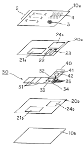
As shown in Figs. 2a to 2c and fig. 3, this,embodiment isaonstructed
of a sheet-like audio information r.ecording/reproducing section 30 capable of
recording/reproducing audio information sandwiched between two support
sheets 20a, 20b made of a flexible and thin material such as paper base
',. material with the support sheets 20a, 20b between which the audio
information recording/reproducing section 30 is sandwiched being further
sandwiched between two surface sheets 10a, 10b having the same outside
shapes as those of the support sheets 20a, 20b, made of a flexible and thin
material such as paper base material. The surface sheets 10a, 10b, support
sheets 20a, 20b and audio information recording/reproducing section 30 are
bonded to one another through adhesive work applied to the front and back
of the support sheets 20a, 20b. This adhesive work can be fEalized, for
example, by pasting a double-faced tape to the front and back of the support
sheets 20a, 20b or applying a hot-melt type adhesive thereto.
Furthermore, the audio information recording/reproducing section 30
is constructed of a sheet-like audio information output section 40 made up of
a piezo-electric element 41, a diaphragm 42 and a film sheet which will be
described later, for outputting recorded audio information, an audio substrate
32 mounted with a thin IC chip 34 which is audio information recording
means for recording audio information and a thin switch 33 which is operating
means operated for outputting the audio information recorded in the 4C chip
34 from the audio information output section 40, and flexible paper batteries
31 connected to the audio substrate 32, for supplying power to the audio
substrate 32, and the audio substrate 32 is further provided with connection
terminals 35 for inputting audio information to the IC chip 34 from ou#side.
37
CA 02621213 2008-03-10
In this way, the audio information recording/reproducing section 30 has
sheet-like structure. Here, the audio substrate 32 is a flexible, thin
substrate
made of fiberglass reinforced plastics (FRP), polyethylene terephthalate
(PET), polyimide or lead frame, etc., with the IC chip 34 bonded by means of
anisotropic/conductive adhesive (ACP), anisotropic/conductive film (ACF),
wire bonding or the like.
Furthermore, when superimposed with the audio information
recording/reproducing section 30, the support sheet 20a is provided with
holes 21 a, 22, 23, 24a in areas facing the paper batteries 31, switch 33, IC
chip 34 and audio information output section 40, respectively. Furthermore,
when superimposed with the audio information r+ecording/reproducing section
30, the support sheet 20b is provided with holes 21b, 24b in areas facing the
paper batteries 31 and audio information output section 40, respectively.
In this way, the holes 21 a, 22, 23, 24a are formed in the areas of the
support sheet 20a facing the paper batteries 31, switch 33, IC chip 34 and
audio information output section 40, and the holes 21 b, 24b are formed in the
areas of the support sheet 20b facing the paper batteries 31 and audio
information output section 40, which reduces the difference in thickness
between the areas where the paper batteries 31, switch 33, IC chip 34 and
audio information output section 40 and the other areas, improves flatness of
the surface sheets 10a, 10b and facilitates printing of information on the
surface sheets 10a, 10b. Furthermore, by making the total thickness of the
support sheets 20a, 20b equivalent to or greater than the thickness of the
thickest part of the audio information recording/reproducing section 30, it is
possible to make the surface sheets 10a, 10b substantially flat. In this case,
by sandwiching the thin parts of the audio information recording/reproducing
38
CA 02621213 2008-03-10
section 30, for example, the area of the audio substrate 32 between the
support sheets 20a, 20b, the audio substrate 32 is fixed. Since the area of
the paper batteries 31 is connected to the audio substrate 32, this area need
not be sandwiched between the support sheets 20a, 20b. Furthermore,
since the surface sheets 10a, 10b are pasted to the support sheets 20a, 20b,
even when the audio information recording/reproducing section 30 has
projections and depressions, the surface sheets 10a, 10b may be recessed
by being pressed, but when there is no pressing force as in the case of an
ink-jet type, the surface sheets 10a, 10b can maintain the flatness, and
thereby allows printing as well.
Fig. 4a illustrates the support sheet 20a shown in Figs. 2a to 2c and
Fig. 3 and audio information recording/reproducing section 30 laminated
together and Fig. 4b illustrates the support sheet 20b shown in Figs. 2a to 2c
and Fig. 3 and the audio information recording/reproducing section 30
laminated together.
As shown in Fig. 4a, the hole 21 a formed in the area of the support
sheet 20a facing the paper batteries 31 is smaller than the paper ba#teries 31
and the hole 22 formed in the area facing the switch 33 is larger than the
switch 33, the hole 23 formed in the area facing the IC chip 34 is larger than
the IC chip 34 and the hole 24a formed in the area facing the audio
information output section 40 is larger than the audio information output
section 40.
Furthermore, as shown in Fig. 4b, the hole 21b formed in the area of
the support sheet 20b facing the paper batteries 31 is smaller than the paper
batteries 31 and the hole 24b formed in the area facing the audio information
output section 40 is smaller than the audio information output section 40.
39
CA 02621213 2008-03-10
In this way, the audio information recording/reproducing section 30 is
laminated with only parts thereof sandwiched between the two support
sheets 20a, 20b from front and back and fixed through adhesive work applied
to the front and back of the support sheets 20a, 20b.
Furthermore, of the two surface sheets 10a, 10b, the surface sheet
10a facing the switch 33 and IC chip 34 through the holes 22, 23 of the
support sheet 20a is provided with an information display area 2 whe-re
address information, etc., is printed when this audio message transfer sheet
1 is mailed and the area facing the switch 33 through the hole 22 of the
support sheet 20'a is provided with a printed playback button 3 for operating
the switch 33. Furthermore, in the area facing the audio information output
section 40 through the hole 24a of the support sheet 20a, an audio output
area 4 made up of an array of fine holes for outputting audio output from the
audio information output section 40 is formed. Even when the'front and
back of the audio information output section 40 are covered with the surface
sheets 10a, 10b, the formation of the audio output area 4 made up of an
array of fine holes can compensate for a reduction of sound volume output
from the audio information output section 40. In the audio output area 4,
holes of 0.1 mm in diameter are formed horizontally and vertically at
intervals
of 1.5 mm through laser beam machining. Therefore, unlike punching or
perforation using needles, etc., no burrs are formed and the holes are never
clogged with burrs. Furthermore, in Fig. 1, though the information display
area 2 is not provided above the audio output area 4, information including
the playback button 3 is actually printed over the entire surface of the
surface
sheet 10a, and therefore the information display area 2 may also be provided
above the audio output area 4. Furthermore, instead of providing the
,6o
CA 02621213 2008-03-10
playback button 3 on the surface sheet 1'Oa by printing, it is also possible
to
paste a seal to the area facing the switch 33 after information is printed on
the surface sheet 10a.
Here, in the case of the audio message transfer sheet 1 structured as
described above, the audio information recording/repFoducing section 30 is
laminated with only part thereof sandwiched between the two support sheets
20a, 20b from front and back as mentioned above and fixed through
adhesive work applied to the front and back of the support sheets 20a, 20b.
Since the support sheets 20a, 20b are provided with holes 21a, 21b, 22, 23,
24a, 24b in the areas facing the paper batteries 31, switch 33, IC chip 34 and
audio information output section 40 of the audio information
recording/reproducing section 30, when the support sheets 20a, 20b and the
audio information recording/reproducing section 30 are laminated, it is
necessary to precisely align the holes 21 a, 22, 23, 24a formed in the support
sheet 20a with the holes 21 b, 24b formed in the support sheet 20b.
Therefore, the support sheets 20a, 20b may be made up of one sheet
so that two support sheets 20a, 20b are constructed by foiding this one sheet
and the holes 21 a, 22, 23, 24a formed in the support sheet 20a are aligned
precisely with the holes 21 b, 24b formed in the support sheet 20b.
Fig. 5a illustrates a structure of the two support sheets 20a, 20b
shown in Fig. 2c and Fig. 3 constructed of one sheet and Fig. 5b illustrates
how the sheet is folded along the bend line 25 shown in Fig. 5a.
As shown in Figs. 5a, 5b, the two support sheets 20a, 20b shown in
Fig. 2c and Fig. 3 are mutually connected along the half-cut bend line 25, the
support sheets 20a, 20b are folded along the bend line 25 so that the audio
information recording/reproducing section 30 is sandwiched between these
41
CA 02621213 2008-03-10
two support sheets 20a, 20b and the audio information recording/reproducing
section 30 is fixed through adhesive work a=pplied to both surfaces of the
support sheets 20a, 20b. In this way, the holes 21a, 22, 23, 24a formed in
the support sheet 20a are precisely aligned with the holes 21b, 24b formed in
the support sheet 20b.
The structure of the audio information output section 40 will be
explained in detail below.
Fig. 6 illustrates the structure of the audio information output section
40 shown in Fig. 2b and is a cross-sectional view around the audio
1 o information output section 40 of the audio message transfer sheet I shown
in
Fig. 2b.
As shown in Fig. 6, the audio information output section 40 in this
embodiment is constructed of a flexible piezo-electric element 41 lor
outputting audio information recorded in the IC chip 34, a flexible fiim sheet
43 pasted to one side of the piezo-electric element 41 and a flexible
diaphragm 42 pasted to the film sheet 43 and made of styrene paper, etc., for
amplifying vibration of the piezo-electric element 41. Here, the diameter of
the film sheet 43 is designed to be greater than the diameter of the piezo-
electric element 41, and therefore when the piezo-electric element 41 is
pasted to the film sheet 43, an area where the piezo-electric element 41 is
not pasted and exposed remains around the piezo-electric element 41 on the
surface of the film sheet 43 to which the piezo-electric element 41 is not
pasted. Furthermore, the diaphragm 42 is designed to have a hole having a
diameter greater than that of the piezo-electric element 41 and smaller than
the diameter of the film sheet 43, and therefore the diaphragm 42 can be
pasted to only the film sheet 43 so that the piezo-electric element 41 can fit
42
CA 02621213 2008-03-10
into this hole on the surface of the film sheet 43 to which the piezo,electric
element 41 is pasted. This diaphragm 42 is bonded to the support sheet
20b in the area out of the surface to which the film sheet 43 is pasted where
the film sheet 43 is not pasted through adhesive work applied to both sides of
the support sheet 20b. This prevents the thickness of the area where the
audio information output section 40 is provided from increasing and causes
the audio information output section 40 to be fixed to the surface sheets 10a,
10b without being bonded, thus avoiding the vibration of the piezo-electric
element 41 and diaphragm 42 from being interfered. Furthermore, setting
the length of one side of the diaphragm 42 to, for example, 2.8 times the
diameter of the piezo-electric eiement 41 can obtain the maximum sound
volume effect of audio information output from the piezo-electric element 41.
The audio information output section 40 structured in this way can also .
function as a microphone for inputting audio information, and in #hat case, a
switch (not shown) for inputting audio information through the audio
information output section 40 needs to be provided on the audio substrate 32.
Furthermore, for the piezo-electric element 41, it is possible to use a PZT-
PMN based (lead-zirconate-titanate + lead magnesium niobate) material
having a diameter of 27 mm, thickness of 0.16 mm.
The structure of the periphery of the switch 33 will be expfained in
detail below.
Fig. 7 is a cross-sectional view of the periphery of the switch 33 of the
audio message transfer sheet 1 shown in Fig. 2b.
The switch 33 shown in Fig. 2b has flexibility. Furthermore, as
shown in Fig. 7, of the support sheets 20a, 20b in the area where the swkch
33 is mounted, only the support sheet 20a is provided with a hole 22 in the
43
CA 02621213 2008-03-10
area facing the switch 33, and therefore the audio substrate 32 is
sandwiched and fixed by the two support sheets 20a, 20b around the swi#ch
33, while in the area of the audio substrate 32 where the switch 33 is
mounted, the audio substrate 32 is mounted on one suppott sheet 20b and
fixed through adhesive work applied to both sides of the support -sheet 20b.
Here, if the height of the switch 33 is assumed to be smaller than the
thickness of the support sheet 20a, the switch 33 is surrounded by the
support sheet 20a which is thicker than the height of the switch 33, which
avoids the switch 33 from being operated when a force majeure is applied
from outside. When the audio message transfer sheet is passed through a
destination sorter using postal code (mail-sorting system), this prevents the
playback button 3 from being pressed and the paper batteries 31 from being
uselessly consumed or audio information recorded in the IC chip 34 from
being overwritten or erased during delivery.
A method of recording audio information in the above described audio
message transfer sheet 1 will be explained below.
As described above, audio information may be recorded in the I.C chip
34 through the audio information output section 40, but in that case, noise
may be mixed into the audio information, drastically degrading tk-e qualityof
sound recorded in the IC chip 34. Therefore, the connection terminaJs 35
provided on the audio substrate 32 are connected to the audio input source
so that the audio information is recorded in the IC chip 34 through the
connection terminals 35, thus making it possible 4o record the audio
information in the IC chip 34 without any noise getting therein. In this case,
instead of connecting the paper batteries 31 to the audio substrate 32, if the
audio substrate 32 is supplied with power from outside through the
~4
CA 02621213 2008-03-10
connection terminals 35, the paper bafteries 31 will not be wnsumed when
audio information is recorded in the IC chip 34.
The above described audio message transfer sheet 1 may be formed
into a postal card size and used as mail or may be formed into a car~d si-ze
and used as a business card or a message card with audio, etc.
(Second embodiment)
Fig. 8a is a plan view of an audio message transfer sheet according to
a second embodiment of the present invention, Fig. Bb illustrates an inner
structure of the audio message transfer sheet shown in'Fig. 8a and "Fig. 8c is
a cross-sectional view along the line A-A' shown in Fig. 8a.
As shown in Figs. 8a to 8c, this embodiment differs from the first
embodiment only in that the audio substrate 32 is provided wi#h a switch 33b
to be pressed when audio information is recorded in the IC chip 34 and a
recording button 3b is printed on an area facing the switch 33b of the surface
sheet 10a. As in the case of the playback button 3a, the recording button 3b
may not necessarily be printed on the surface sheet 10a but it is also
possible to print information on the surface sheet 10a and then -paste a seal
to the area facing the switch 33b.
In the audio message transfer sheet 101 structured as described
above, when audio information is recorded in the IC chip 34, if audio
information is input through the audio information output section 40 with the
recording button 3b provided on the surface sheet 10a held down, the audio
information input through the audio information output section 40 is recorded
in the IC chip 34 and if the playback button 3a provided on the eurface sheet
10a is pressed, the audio information recorded in the IC chip 34 is output
through the audio information output section 40.
CA 02621213 2008-03-10
(Third embodiment)
Fig. 9a is a plan view of an audio message transfer sheet according to
a third embodiment of the present invention, Fig. 9b illustrates an inner
structure of the audio message transfer sheet 201 shown in Fig. '9a and Fig.
9c is a cross-sectional view along the line A-A' shown in Fig. 9a.
Furthermore, Fig. 10 illustrates a recording area of the IC chip 234 shown in
Fig. 9b.
As shown in Figs. 9a, 9b, this embodiment is equivalent to the first
embodiment further provided with three switches 233a to 233c to be pressed
when audio information recorded in an IC chip 234 is reproduced on an audio
substrate 32 and three playback buttons 203a to 203c printed in the areas
facing the switches 233a to 233c on a surface sheet 10a. furthermore, as
shown in Fig. 10, the recording area of the IC chip 234 in which audio
information is recorded is divided into three areas 234a to 234c and different
pieces of audio information are recorded in the respective areas 234a to
234c.
In the audio message transfer sheet 201 structured as described
above, of the three playback buttons 203a to 203c, when the pfayback button
203a is pressed, for example, the audio information recorded in the recording
area 234a of the IC chip 234 out of the audio information recorded in the IC
chip 234 is output from the audio information output section 40, when the
playback button 203b is pressed, the audio information recorded in the
recording area 234b of the IC chip 234 out of the audio information recorded
in the IC chip 234 is output from the audio information output section 40, and
when the playback button 203c is pressed, the audio information recorded in
the recording area 234c of the IC chip 234 out of the audio information
nh
CA 02621213 2008-03-10
recorded in the IC chip 234 is output from the audio information output
section 40.
In this way, by recording a plurality of pieces of audio information in
one IC chip 234 and selectively pressing the plurality of playback buttons
203a to 203c provided on the surface sheet 10a, it is possible to selectively
output a plurality of pieces of audio information recorded in the IC chip 234
from the audio information output section 40.
This embodiment is provided with three playback buttons 203a to
203c and switches 233a to 233c and the information r,eoording a~r=ea in #he IC
chip 234 is divided into three areas 234a to 234c, but the number of piayback
buttons and switches and the number of portions into which the information
recording area in the IC chip is divided is not limited to 3.
(Fourth embodiment)
Fig. 11 a is a plan view of an audio message transfer sheet according
to a fourth embodiment of the present invention, Fig. 11b illustrates an inner
structure of the audio message transfer sheet 301 shown in Fig. 11a and fig.
11 c is a cross-sectional view along the line A-A' shown in Fig. 11 a.
As shown in Figs. 11 a to 11 c, this =embodiment is equivaient to the
first embodiment further provided with two audio information output sections
340a, 340b on an audio information recording/reproducing section 330, and a
surface sheet 310a is provided with audio output areas 304a, 304b for
outputting audio information from these audio information output sections
340a, 340b through bend lines 305a, 305b. Furthermore, support sheets
320a, 320b are divided into three portions so as to correspond 4o three
adjoining areas along the bend lines 305a, 305b of the surface sheet 310a so
that the audio output areas 304a, 304b can be folded along the bend lines
47
CA 02621213 2008-03-10
305a, 305b. An information display area 2 is provided so as to span three
adjoining areas along the bend lines 305a, 305b.
In the audio message transfer sheet 301 structured as described
above, audio information recorded in an IC chip 34 is output from the two
audio information output sections 340a, 340b, and therefore it is possible to
increase the sound volume of the output audio information compared to the
first embodiment. In this case, a piezo-electric element 41 is used as a
device for outputting the audio information recorded in the IC chip 34, and
therefore even when the audio information recorded in the ICchip 34 is
output from the two audio information output sections 340a, 340b, the life of
paper batteries 31 is not shortened.
Furthermore, since the two audio output areas 304a, 304b ar.e
foldable along the two bend lines 305a, 305b, when the audio information
recorded in the IC chip 34 is not output from the audio information output
sections 340a, 340b, the audio output areas 304a, 304b can be folded along
the bend lines 305a, 305b so as to improve the portability of the audio
message transfer sheet 301. For example, setting the size of the sheet
when the audio output areas 304a, 304b are folded along the bend lines
305a, 305b to a business card size allows the audio message transfer sheet
301 to be housed in a business card case, etc.
Furthermore, it is also possible to cause different pieces of audio
information to be output from the two audio information output sections 340a,
340b. This allows the receiver of the audio message transfer sheet 301 to
listen to the information recorded in the IC chip 34 as
stereophonic'aroadcast,
for example.
This embodiment is provided with two audio information output
48
CA 02621213 2008-03-10
sections 340a, 340b, but the number of audio information output sections is
not limited to 2. Furthermore, an information display area 2 is provided
extending over three adjoining areas along the bend lines 305a, 305b, but it
is also possible to provide the information display area in only some of the
adjoining three areas along the bend lines 305a, 305b.
Furthermore, according to this.embodiment, one audio substrate 32 is
connected to the two audio information output sections 340a, 340b, but it is
also possible to provide one audio substrate for each of the audio information
output sections 340a, 340b and output audio information recorded in IC chips
provided on the audio substrates by operating the respective switches
provided on the audio substrates.
Furthermore, according to this embodiment, the support sheets 320a,
320b are divided into three portions so as to correspond to the three
adjoining areas along the bend lines 305a, 305b of the surface sheet 310a,
but it is also possible to further divide the support sheets divided so as to
correspond to the three adjoining areas along the bend lines 305a, 305b.
Adopting such a structure further increases the degree of freedom in bending
or folding the audio message transfer sheet 301. Dividing the support sheet
into a plurality of portions in this way is not limited to this embodiment,
but
can also be applied to the above described first to fourth embodiments and
fifth and sixth embodiments which will be described later.
(Fifth embodiment)
Fig. 12a is a plan view of an audio message transfer sheet according
to a fifth embodiment of the present invention, Fig. 12b illustrates an inner
structure of the audio message transfer sheet shown in Fig. 12a and fig. 12c
is a cross-sectional view along the line A-A' shown in Fig. 12a.
49
CA 02621213 2008-03-10
As shown in Figs. 12a to 12c, this embodiment only differs from the
first embodiment in that the outside shapes of support sheets 420a, 420b are
smaller than the outside shapes of the surface sheets 10a, 1-0b.
Thus, the present invention is equally applicable to a case where the
outside shapes of the support sheets 420a, 420b are smaller than the outside
thapes of the surface sheets 10a, 10b and a case where the outside shapes
of the support sheets 420a, 420b are greater than the outside shapes of the
surface sheets 10a, 10b.
(Sixth embodiment)
Fig. 13a is a plan view of an audio message transfer sheet according
to a sixth embodiment of the present invention, Fig. 13b illustrates an inner
structure of the audio message transfer sheet shown in Fig. 13a and fig. 13c
is a cross-sectional view along the line A-A' shown in fig. 13a.
As shown in Figs. 13a to 13c, this embodiment corresponds to the first
embodiment with an ink receiving layer 511 superimposed on the surfaoe of
a surface sheet 10a not facing a support sheet 20a.
In the audio message transfer sheet 501 structured as described
above, the ink receiving layer 511 is laminated on the surface of the surface
sheet 10a not facing the support sheet 20a on which the information disptay
area 2 is provided, and therefore when information is printed on an
information display area 2 using an ink-jet printer, it is possible to print
the
information clearly on the information display area 2.
A method of manufacturing the above described audio message
transfer sheet 501 will be explained below.
Figs. 14a to 14f illustrate a method of manufacturing the audio
message transfer sheet 501 shown in Figs. 13a to 13c.
CA 02621213 2008-03-10
First, the ink receiving layer 511 as shown in Fig. 14b is superimposed
on the surface sheet 10a as shown in'Fig. 14a. When the surface sheet 10a
is cut from continuous forms paper into single sheets, if the ink receiving
layer 511 is superimposed on the surface sheet 10a of continuous forms
paper, the ink receiving layer 511 can be easily superimposed.
Next, as shown in Fig. 14c, holes of 0.1 mm in diameter are formed in
the surface sheet 10a on which the ink receiving layer 511 is superimposed
through laser beam machining as described above to provide an audio output
area 4.
Furthermore, as shown in Fig. 14d, an audio information
recording/reproducing section 30 is sandwiched between two support sheets
20a, 20b.
Then, as shown in Fig. 14e, the support sheets 20a, 20b between
which the audio information recording/reproducing section 30 is sandwiched
are further sandwiched between the surface sheets 10a, 10b.
This completes an audio message transfer sheet with no information
printed on the surface of the surface sheet 10a, and then as shown in fig.
14f, a playback button 3 is printed on the surface sheet 10a on which the ink
receiving layer 511 is superimposed and information is printed on the
information display area 2 using an ink-jet printer.
This embodiment has explained the case where the ink receiving layer
511 is superimposed on the surface sheet 10a of the audio message transfer
sheet 1 shown in the first embodiment as an example, -but it is also possible
to superimpose the ink receiving layer 511 on the surface sheet 10b of the
audio message transfer sheet 1 or it is also possible to superimpose the ink
receiving layer 511 only on the surface sheet 1'Oa or on the surface sheets
51
CA 02621213 2008-03-10
10a, 10b of the audio message transfer sheet shown in the above described
second to fifth embodiments.
In the inventions shown in the above described first to sixth
embodiments, the audio information recording/reproducing means capabie of
recording/reproducing audio information has a sheet-like structure, and of the
breas of the two support sheets between which the audio information
recording/reproducing means is sandwiched from front and back, bonded
together, facing the audio information recording/reproducing means, the
audio information recording/reproducing means is sandwiched 4om front and
back between only portions of those areas, and therefore the sheetcan be
easily bent or folded and information can be printed on the surface sheet.
Furthermore, when the two support sheets have the same outside
shapes as those of the surface sheets, the thickness of the entire audio
message transfer sheet can be made substantially uniform.
Furthermore, when the two support sheets are each divided into a
plurality of portions, it is possible to increase the degree of freedom in
bending and folding the audio message transfer sheet.
Furthermore, when the two support sheets are connected together
along a bend line, the two support sheets can be easily aligned with each
other.
Furthermore, in the case of the structure that the audio information
outputting means provided on the audio information recording/reproducing
means for outputting audio information is constructed of a piezo-efectfic
element for outputting audio information, a film sheet having a larger
diameter than that of the piezo-electric element, pasted to one surface of the
piezo-electric element and a diaphragm having a hole with a diameter larger
52
CA 02621213 2008-03-10
than the diameter of the piezo-electric element and smaNer than the diameter
of the film sheet, pasted to the film sheet so that the -piezo-etectric
element
fits into the hole, wherein the diaphragm is bonded to the support shee#sonly
in the area not bonded to the film sheet of the surface of bonding with the
film
sheet, it is possible to prevent the thickness of the area in which the audio
1 information outputting means is provided from increasing and cause the
audio information outputting means to be fixed without being bonded to the
surface sheet and thereby prevent vibration of the piezoelectric element and
diaphragm from being interfered.
Furthermore, in the case of the structure that two support sheets
sandwich the audio information recording/reproducing means around the
operating means and the audio information recording/reproducing means is
mounted on one support sheet in the area where the operating means is
provided, if the height of the operating means is smaller than the thickness
of
the support sheet, the operating means is surrounded by the support sheet
whose thickness is greater than the height of the operating means, which
makes it possible to avoid the operating means from being operated when a
force majeure is applied from outside.
Furthermore, in the case of the structure that an ink -receiving iayer is
superimposed on the surface not facing at least one support sheet of the two
surface sheets, if information is printed on the surface sheet using an ink-
jet
printer later, it is possible to clearly print information on the surface
sheet.
Furthermore, in the case of the structure that this ink receiving layer is
superimposed on the surface sheet before the support sheets between which
the audio information recording/reproducing means is sandwiched are
sandwiched between the surface sheets, it is possibie to superimpose the ink
53
CA 02621213 2008-03-10
receiving layer with excellent flatness of the surface sheets and when the
surface sheet is cut from continuous forms paper into single pieces, the ink
receiving layer is superimposed on the surface sheet of the aontinuoUs forms
paper, facilitating the superimposition of the ink receiving layer.
(Seventh embodiment)
Fig. 15a is a plan view of an audio information output sheet according
to a seventh embodiment of the present invention, Fig. 15b illustrates an
inner structure of the audio information output sheet shown in Fig. 15a and
Fig. 15c is a cross-sectional view along the line A-A' shown in Fig. 15a.
Furthermore, Fig. 16 illustrates a laminated structure of the audio
information
output sheet 1 shown in Figs. 15a to 15c.
As shown in Figs. 15a to 15c and Fig. 16, this embodiment is
constructed in such a way that a sheet-like audio information
recording/reproducing section 1030 capable of recording/reproducing audio
information is sandwiched between two support sheets 1020a, 1020b made
of a flexible, thin base material such as paper base material, the support
sheets 1020a, 1020b between which the audio information
recording/reproducing section 1030 is sandwiched are sandwiched between
two surface sheets 1010a, 1010b made of a flexible, thin base material such
as paper base material and the sheets can be folded along the areas in
which bend lines 1015a, 1015b of the surface sheets 1010a, 1010b are
provided as bend lines. The surface sheets 1010a, 1010b, support sheets
1020a, 1020b and audio information recording/reproducing section 1030 are
bonded to one another through adhesive work applied to the front and back
of the support sheets 1020a, 1020b. This adhesion can be realized by
pasting a double-faced tape to the front and back of the support sheets
54
CA 02621213 2008-03-10
1020a, 1020b or applying a hot-melt type adhesive thereto.
Furthermore, the audio information r,ecording/reproducing section
1030 is constructed of a sheet-like audio information output section 1040 for
outputting recorded audio information, an audio substrate 1032 mounted with
a thin IC chip 1034 which is an audio information recording section for
~~recording audio information and a thin switch 1033 which is operated to
output the audio information recorded in the IC chip 1034 from the audio
information output section 1040, and flexible paper batteries 1031 connected
to the audio substrate 1032 for supplying power to the audio substrate 1,032
and a connection substrate 1036 made of a polyimide film on which a wiring
pattern 1037 for connecting the IC chip 1034 and the audio information
output section 1040 is formed, and the audio substrate 1032 is further
provided with connection terminals 1035 for inputting/outputting audio
information to/from the IC chip 1034 from/to outside. In this way, the audio
information recording/reproducing section 1030 has a sheet-like structure.
Here, the audio substrate 1032 is a flexible, thin substrate made of
fiberglass
reinforced plastics (FRP), polyethylene terephthalate (PET), polyitnide or
lead frame, etc., with the IC chip 1034 bonded thereto by means of
anisotropic/conductive adhesive (ACP), anisotropic%onductive film (ACr) or
wire bonding. A connection substrate 1036 is not limited to one made up of
a polyimide film but any film made of resin such as PET having at least
flexibility can be used.
Furthermore, when superimposed on the surface sheet 1010a, the
support sheet 1020a is divided into two portions through the area facing the
bend line 1015a and when superimposed on the audio information
recording/reproducing section 1030, holes 1021 a, 1022, 1023, 1024a are
CA 02621213 2008-03-10
formed in the areas facing the paper ba#teries 1031, switch 1033, IC chip
1034 and audio information output section 1040 respectively. Furthermore,
when superimposed on the surface sheet 1010b, the support sheet 1020b is
divided into two portions through the area facing the bend line 1015b and
when superimposed on the audio information recording/repraducing section
i
11030, holes 1021 b, 1024b are formed in the areas facing the paper batteries
1031 and audio information output section 1040 respectively.
Furthermore, the connection substrate 1036 for connecting the IC chip
1034 and audio information output section 1040 is provided sandwiched
between the divided areas of the support sheets 1020a, 1020b.
Fig. 17a illustrates a laminated structure of the support sheet 1020a
and audio information recording/reproducing section 1030 shown in Figs. 15b,
15c and Fig. 16 and Fig. 17b illustrates a laminated structure of the support
sheet 1020b and audio information recording/reproducing section 1030
shown in Figs. 15b, 15c and Fig. 16.
As shown in Fig. 17a, the hole 1021 a formed in the area of the
support sheet 1020a facing the paper batteries 1031 is smaller than the
paper batteries 1031 and the hole 1022 formed in the area facing tf-e switch
1033 is greater than the switch 1033, the hole 1023 forrned in the area facing
the IC chip 1034 is greater than the IC chip 1034 and the hoie 1 024a formed
in the area facing the audio information output section 1040 is greater than
the audio information output section 1040.
Furthermore, as shown in Fig. 17b, the hole 1021 b formed in the area
of the support sheet 1020b facing the paper batteries 1031 is -smaller than
the paper batteries 1031 and the hole 1024b formed in the area facing the
audio information output section 1040 is smaller than the audio information
56
CA 02621213 2008-03-10
output section 1040.
In this way, the audio information recording/reproducing section 1030
is laminated so that only part thereof is sandwiched between the two support
sheets 1020a, 1020b from front and back and fixed through adhesive work
applied to the front and back of the support sheets 1020a, 1020b.
Furthermore, of the two surface sheets 1010a, 1010b, the surface
sheet 1010a facing the switch 1033 and IC chip 1034 through the holes 1022,
1023 of the support sheet 1020a is provided with an information display area
1002 where address information, etc., is printed when this audio 4message
transfer sheet 1001 is used, for example, as a business card and the area
facing the switch 1033 through the hole 1022 of the support sheet 1.020a is
provided with a playback button 1003 for operating the switch 1033.
Furthermore, in the area facing the audio information output section 1040
through the hole 1024a of the support sheet 1020a, an audio output area
1004 made up of an array of fine holes for outputting audio output from the
audio information output section 1040 is formed and the area where the
audio output area 1004 is formed is foldable along the bend line 1015a with
respect to the other areas. Even when the front and back of the audio
information output section 1040 are covered with the surface sheets 1010a,
1010b, the formation of the audio output area 1004 made up of an array of
fine holes can compensate for a reduction of sound volume output from the
audio information output section 1040. In the audio output as.ea 1004, holes
of 0.1 mm in diameter are formed horizontally and vertically at intervals of
1.5
mm through laser beam machining.
A method of use of the audio information output sheet 1001 structured
as described above will be explained below.
57
CA 02621213 2008-03-10
Fig. 18a illustrates the audio information output sheet 1001 shown in
Figs. 15a to 15c and Fig. 16 not in use and Fig. 18b illustrates the audio
information output sheet 1001 shown in Figs. 15a to 15c and fig. 16 in use.
When the audio information output sheet 1001 shown in figs. 15a to
15c and Fig. 16 is not in use, the audio information output sheet 10,01 is
~
Ifolded along the bend lines 1015a, 1015b as shown in Fig. 18a. In this
condition, the area of the audio information output section 1040 of the audio
information recording/reproducing section 1030 sandwiched between the
support sheets 1020a, 1020b and the surfaces sheet 1010a, 1010b is folded
along the bend lines 1015a, 1015b with respect to the other areas, and if the
size of the audio information output sheet 1001 in this condition is assumed
to be a business card size, it is possible to insert the folded audio
information
output sheet 1001 into a business card case, etc., and thereby improve
portability. Furthermore, in this condition, the audio output area 1004
provided on the surface sheet 1010a is not exposed to output the audio
output from the audio information output section 1040 to outside.
Furthermore, since the IC chip 1034 and the audio information output section
1040 are connected by a wiring pattern 1037 formed on the connection
substrate 1036 sandwiched between the divided areas of the support sheets
1020a, 1020b, even if the audio information output sheet 1001 can be folded
along the folded sections 1015a, 1015b, it is possible to avoid the wiring
between the IC chip 1034 and the audio information output section 1040 from
being broken. Furthermore, when the audio information output sheet 1001
is folded as shown in Fig. 18a, if the spacing between the divided areas of
the support sheet 1020a, 1020b is adjusted to be equal to or greater than the
distance between the surface sheets 1010b which become outside in the
5el
CA 02621213 2008-03-10
folded section, that is, at least twice the thickness of the audio information
output sheet 1001, it is possible to keep the folding state.
When the audio information output sheet 1001 shown in Figs. 1,5a to
15c and Fig. 16 is in use, as shown in Fig. 18b, when the folded audio
information output sheet 1001 is opened and the playback button 1003 is
pressed, the audio information recorded in the IC chip 1034 of the audio
information recording/reproducing section 1030 is output from the audio
information output section 1040. Here, in this condition, the audio output
area 1004 provided in the surface sheet 1010a is exposed to output the
audio output from the audio information output section 1040 to outside.
Furthermore, if the audio information output sheet 1001 is keptopen so that
the adjoining areas form a certain angle along the bend line 1015a as shown
in Fig. 18b, it is possible to output audio information with the audio
information output sheet 1001 placed on a desk, etc.
In this way, the audio information output sheet 1001 is folded when
not in use and the audio information output sheet 1001 is opened and audio
information is output when the audio information output sheet 1001 is in use,
so that it is possible to miniaturize the card while securing the sound votume
of audio information output.
2 0 According to this embodiment, only the area of the audio information
recording/reproducing section 1030 in which the audio information output
section 1040 is sandwiched between the support sheets 1020a, 1020b and
surface sheets 1010a, 1010b is foldable with respect to the other areas, but
it
is also possible to adopt a structure that the area of the audio information
recording/reproducing section 1030 in which the audio information output
section 1040 and part of the area other than the audio information output
59
CA 02621213 2008-03-10
section 1040 are sandwiched is foldable with respect to the other areas. In
that case, if the audio substrate 1032 is made up of a polyimide frlm as in
the
case of the connection substrate 1036, even if it is -sandwiched between the
surface sheets 1010a, 1010b and support sheets 1020a, 1020b so that the
audio substrate 1032 spans the bend lines 1015a, 1015b, it is possible to
secure durability with respect to the folding operation of the audio
information
output sheet 1001 along the bend lines 1015a, 1015b.
Furthermore, according to this embodiment, the playback but#on 1003
which is pressed to output audio information recorded in the IC chip 1034
from the audio information output section 1040 is provided at such a position
that the playback button 1003 is exposed even when the audio infomnation
output sheet 1001 is folded along the bend lines 1015a, 1015b, but it is also
possible to provide the playback button 1003 in the area of the surface sheet
1010a where the playback button 1003 is not exposed when the audio
information output sheet 1001 is folded along the bend lines 1015a, 1015b.
In that case, it is possible to prevent the playback button 1003 from being
pressed when the audio information output sheet 1001 is foidred along the
bend lines 1015a, 1015b and avoid unnecessary consumption of the paper
batteries 1031.
Furthermore, it is also possible to make the audio information output
section 1040 function as a microphone for inputting audio information and
record audio information in the IC chip 1034 through the audio information
output section 1040. However, in that case, the audio substrate 1032 needs
to be provided with a switch (not shown) for inputting audio information
through the audio information output section 1040.
(Eighth embodiment)
0 0
CA 02621213 2008-03-10
Fig. 19a is a plan view of an audio information output sheet according
to an eighth embodiment of the present invention, Fig. 19b illustrates an
inner
structure of the audio information output sheet 1101 shown in Fig. 19a and
Fig. 19c is a cross-sectional view along the line A-A' shown in Fig. 19a.
As shown in Figs. 19a to 19c, this embodiment differs from the
seventh embodiment in that two audio information output sections 1140a,
11 40b are connected to an audio substrate 1032 through wiring patterns
1037a, 1037b formed on connection substrates 1036a, 1036b and the areas
where the audio information output sections 1140a, 1140b are sandwiched
1 o between support sheets 1120a, 1120b and surface sheets 1110a, 1110b are
foldable along bend lines 1105a, 1115a with respect to the other area. The
support sheets 1120a, 1120b are aiso divided into three areas through areas
facing the bend lines 11 05a, 1115a provided on the surface sheet 1110a as
in the case of the seventh embodiment.
A method of use of the audio information output sheet 1101 structured
as described above will be explained below.
Fig. 20a illustrates the audio information output sheet 1101 shown in
Figs. 19a to 19c not in use and Fig. 20b illustrates the audio information
output sheet 1101 shown in Figs. 19a to 19c in use.
When the audio information output sheet 1101 shown in Figs. 19a to
19c is not in use, the audio information output sheet 1101 is folded along the
bend lines 1105a, 1105b, 1115a, 1115b as shown in Fig. .20a: 1n this
condition, the areas of the audio information recording/feproducing section
1130 in which the audio information output sections 1140a, 1140b are
sandwiched between the support sheets 1120a, 1120b and surface sheets
1110a, 1110b are folded along the bend lines 1105a, 1105b, 1115a, 1115b
r, 1
CA 02621213 2008-03-10
with respect to the other area and if the size of the audio information output
sheet 1101 in this condition is assumed to be a business card si~ze, the
folded
audio information output sheet 1101 can be inserted in a business card case,
etc., which improves portability. Furthermore, in this condition, the audio
output areas 11 04a, 11 04b provided on the surface -sheet 1110a to output
audio output from the audio information output sections 1140a, 1140b to the
outside are not exposed. Furthermore, in this condition, the piayback button
1003 which is pressed to output audio information recorded in the IC chip
1034 from the audio information output sections 1140a, 1140b is notexposed,
and therefore the playback button 1003 is not pressed mistakenly, which
avoids unnecessary consumption of the paper batteries 1031.
Furthermore, when the audio information output sheet 1101 shown in
Figs. 19a to 19c is used, by opening the folded audio information output
sheet 1101 as shown in Fig. 20b and pressing the playback button 1003,
audio information recorded in the IC chip 1034 of the audio information
recording/reproducing section 1130 is output from the audio information
output sections 1140a, 1140b. In this condition, the audio output areas
1104a, 1104b provided on the surface sheet 1110a to output audio output
from the audio information output sections 1140a, 1140b to ou4side are
exposed. Furthermore, when the audio information output sheet 1101 is
kept open so that the adjoining areas form a predetermined angle along the
bend lines 1105a, 1115a as shown in Fig. 20b, it is possible to output audio
information with the audio information output sheet 1101 placed on a desk,
etc. _
In this way, this embodiment adopts a structure foldable three fold
along the bend lines 1105a, 1105b, and therefore it is possible to widely
62
CA 02621213 2008-03-10
secure areas to which audio information is output with respect to the size in
the folded state and thereby realize a large sound volume.
In this embodiment, it is also possible to adopt a s#ructure thattfie
area of the audio information recording/reproducing section 1130 in which the
audio information output sections 11 40a, 1 140b and part of areas other than
the audio information output sections 11 40a, 11 40b are sandwich.,pd is made
foldable with respect to the other area. In that case, if the audio substrate
1032 is made up of a polyimide film, even when the audio substrate 1032 is
sandwiched between the surface sheets 1110a, 1110b and supportsheets
11 20a, 1120b so that the audio substrate 1032 spans the bend lines 1105a,
1115a, it is possible to secure durability with regard to the folding
operation of
the audio information output sheet 1101 along the bend lines 1105a, 1115a.-
Furthermore, it is also possible to make audio information pieces
output from the audio information output sections 1140a, 1140b different from
each other. In this way, it is possible to listen to information recorded in
the
IC chip 1034 as stereophonic broadcast, for example.
Furthermore, this embodiment is provided with two audio information
output sections 1140a, 1140b, but the number of the audio information output
sections 1140a, 1140b is not limited to two. In that case, at least one audio
information output section is made foldable three fold among the two areas
sandwiched between the support sheets 11 20a, 11 20b and surface sheets
1110a, 1110b and the other area. For example, it is possible to adopt a
three-fold structure with four audio information output sections provided,
with
two areas formed with two sets of audio information output sections
sandwiched between the support sheets 11 20a, 1120b and surface sheets
1110a, 1110b and the other area. In this case, too, by adopting a structure
63
CA 02621213 2008-03-10
that different pieces of audio information are output to two areas, it is
possible to listen to information recorded in the -{C chip 1034 as
stereophonic
broadcast, for example.
Furthermore, instead of limiting to a three-fold foldable structure as
with this embodiment, it is also possible to provide areas foldable along bend
lines in areas adjoining the audio output areas 1104a, 1104b along thebend
lines 11 05a, 111 5a, that is, areas where the audio substrate 1032 is
sandwiched in the upper or lower part in the figure. In that case, too, the
support sheets 1120a, 1120b sandwiched between the surface sheets 1110a,
1110b are preferably divided along bend lines, but in that case, too, if the
spacing between the divided areas of the support sheets 11 20a, 11 20b is
adjusted to be equal to or greater than the distanoe between the surface
sheets 1110b which become outside in the folded section when the audio
information output sheet 1101 is folded, it is possible to keep the folding
state.
For example, when areas which are foldable along bend lines are provided in
the upper and lower parts in the figure of the area adjoining the audio output
areas 1104a, 1104b along the bend lines 110'5a, 1115a are provided, the
audio information output sheet 1101 is folded as shown in Fig. 20a first, and
then the above described areas in the upper and lower parts are folded, if the
spacing between the areas adjoining along the bend lines 1105a, 1115a of
the support sheets 1 120a, 11 20b is adjusted to be equal to or greater than
twice the thickness of the audio information output sheet 1101 and the
spacing between the area in which the audio substrate 1032 is sandwiched
between the support sheets 11 20a, 11 20b and areas constituting the upper
and lower parts thereof is adjusted to be at least three times the thickness
of
the audio information output sheet 1101, it is possible to keep the folding
64
CA 02621213 2008-03-10
state.
Furthermore, according to the seventh and eighth embodiments, the
support sheets are divided along the bend line, but the support sheets can
also be made of an easily foldable material so that the support sheets a-re
not
divided.
According to the invention shown in the seventh and eighth
embodiments, the area of the audio information recording/reproducing means
in which at least the audio information output section is incorporated is made
foldable along bend lines and the area in which the audio information output
section is incorporated is folded with respect to the other area so as to
realize
miniaturization, and therefore it is not necessary to reduce the size of the
audio information output section and it is possible to realize miniaturization
while securing a predetermined sound volume.
Furthermore, in the case of the structure that the audio information
recording/reproducing means is made of a sheet-like base material, two
support sheets are bonded together with the audio information
recording/reproducing means sandwiched in between from front and back,
the two support sheets are divided along bend lines and the audio
information recording/reproducing means is sandwiched from front and back
in only some of the areas facing the audio information recording/reproducing
means, it is possible to improve flatness of the surface irrespective of the
foldable structure and thereby facilitate printing of information on the
surface
sheet.
Furthermore, in the case of the structure that the spacing between the
divided areas of the support sheets when the audio information output sheet
is folded is equal to or greater than the distance between the surface sheets
CA 02621213 2008-03-10
which become the outside in the folded section of the two surface sheets, it
is
possible to keep the folding state when the audio information output sheet is
folded along the bend line.
Furthermore, in the case of the structure that the audio information
recording/reproducing means includes a plurality of audio info,rmation output
sections and a plurality of areas each incorporating at least one audio
information output section are made foldable along bend lines with respect to
the other area, it is possible to increase a sound volume of audio information
output without increasing the size of the audio information output sheet in
the
folding state.
(Ninth embodiment)
Fig. 21 a is a plan view of a POP indicator 2001 according to a ninth
embodiment of the present invention and Fig. 21b illustrates an inner
structure of the POP indicator 2001 shown in Fig. 21 a. Furthermore, Fig. 22
illustrates a laminated structure of the POP indicator 2001 shown in Figs. 21
a,
21 b.
As shown in Figs. 21 a, 21 b and Fig. 22, this embodiment is
constructed in such a way that a sheet-like audio information
recording/reproducing section 2030 capable of recording/reproducing audio
information is sandwiched between two support sheets 2020a, 2020b made
of a flexible, thin base material such as paper base material and the support
sheets 2020a, 2020b between which the audio information
recording/reproducing section 2030 is sandwiched are further sandwiched
between a surface sheet 2010a and a back sheet 2010b having the same
2 5 outside shapes as those of the support sheets 2020a, 2020b, made of a
flexible, thin base material such as paper base material. Furthermore, a
66
CA 02621213 2008-03-10
mounting member 2005 for mounting the POP indicator 2001 on an object
such as a showcase is provided. The surface sheet 2010a, back sheet
2010b, support sheets 2020a, 202Ub and audio information
recording/reproducing section 2030 are mutually bonded through adhesive
work applied to the front and back of the support sheets 2020a, 2020b
~ whereby the audio information recording/reproducing section 2030 is pasted
to the surface of the surface sheet 2010a. This adhesive work can be
realized by pasting a double-faced tape to the front and back of the support
sheets 2020a, 2020b or applying a hot-melt type adhesive thereto.
Furthermore, some areas of the surface sheet 2010a, back sheet 2010b,
support sheets 2020a, 2020b and audio information recording/reproducing
section 2030 protrude from other areas.
Furthermore, the audio information recording/reproducing section
2030 is constructed of an audio substrate 2032 mourded with an IC chip
2034 which is audio information recording means and a switch 2033 which is
operating means, an audio information output section 2040 and three paper
batteries 2050a to 2050c and the area of the audio substrate 2032 on which
the switch 2033 is mounted protrudes from the other area.
The IC chip 2034 is designed to record audio information and the
audio information output section 2040 is designed to output the audio
information recorded in the IC chip 2034 when the switch 2033 is pressed.
Furthermore, the three paper batteries 2050a to 2050c are connected in
series by means of an anisotropic/conductive adhesiv.e (ACP) or
anisotropic/conductive film (ACF), both ends -of which are connected to the
2 5 audio substrate 2032 to- serve as a power supply section to supply power.
to
the audio substrate 2032.
67
CA 02621213 2008-03-10
Furthermore, the audio substrate 2032 is provided with connection
terminals 2035 for inputting audio information to the iC chip 2034 from
outside and is a flexible, thin substrate made of fiberglass reinforced
plastics
(FRP), polyimide or lead frame, etc., with the IC chip 2034 connected thereto
by means of an anisotropic/conductive adhesive (ACP),
anisotropic/conductive film (ACF) or wire bonding.
Furthermore, the support sheet 2020a is made of a thin base material
and the thickness thereof is set according to the required durability as
appropriate and when superimposed on the audio information
recording/reproducing section 2030, holes 2021 a, 2022, 2023, 2024a are
formed in the areas facing the paper batteries 2050a to 2050c, swi#ch 2033,
IC chip 2034 and audio information output section 2040 and the area in
which the hole 2022 is formed protrudes from the other areas.
Furthermore, the support sheet 2020b is made of a thin base material,
but the thickness thereof is set according to the required durability as
appropriate and when superimposed on the audio information
recording/reproducing section 2030, holes 2021 b, 2024b are formed in the
areas facing the paper batteries 2050a to 2050c and audio information autput
section 2040 and the area facing the switch 2033 through the audio substrate
2032 protrudes from the other areas.
Fig. 23a illustrates a laminated structure of the support sheet 2020a
and audio information recording/reproducing section 2030 shown in Fig. 22b
and Fig. 23 and Fig. 23b illustrates a laminated structure of the support
sheet
2020b-and audio information recording/r<eproducing section 2030 shown in
Fig. 22b and Fig. 23.
As shown in Fig. 23a, the size of the hole 2021 a formed in the area of
68
CA 02621213 2008-03-10
the support sheet 2020a facing the paper batteries 2050a to 2050c is smaller
than the size of three paper batteries 2050a to 2050c connected, the hole
2022 formed in the area facing the switch 2033 is greater than the swi#ch
2033, the hole 2023 formed in the area facing the IC chip 2034 is greater
than the IC chip 2034 and the hole 2024a formed in the area facing the audio
~ information output section 2040 is greater than the audio information output
section 2040.
Furthermore, as shown in Fig. 23b, the size of the hole 2021 b formed
in the area of the support sheet 2020b facing the paper batteries 2050a to
2050c is smaller than the three paper batteries 2050a to 2050c connected
and the hole 2024b formed in the area facing the audio information output
section 2040 is smaller than the audio information output section,2040.
In this way, the audio information recording/reproducing section 2030
is laminated so that only part thereof is sandwiched between the two support
sheets 2020a, 2020b from the front and back of the sheet and fixed through
adhesive work applied to the front and back of the support sheets 2020a,
2020b.
Furthermore, the surface sheet 2010a is provided with an infiorma#ion
display area 2002 on which advertisement information is printed as a POP, a
playback button 2003 for operating the switch 2033 is provided in the area of
the support sheet 2020a facing the switch 2033 through the hole 2022, an
audio output area 2004 made up of an array of fine holes for outputting audio
output from the audio information output section 2040 is formed in the ar.ea
facing the audio information output section 2040 -through the hoae 2024a of
the support sheet 2020a. Since the audio output area 2004 is formed with
such an array of fine holes, it is possible to compensate for a reduction of
69
CA 02621213 2008-03-10
sound volume output from the audio information output section 2040 even
when the front and back of the audio information output section,2040 are
covered with the surface sheet 2010a and back sheet 2010b. In the audio
output area 2004, holes of 0.1 mm in diameter are formed horizontally and
vertically at intervals of 1.5 mm through laser beam machining. Ther.efore,
unlike punching or perforation using needles, etc., no burrs are formed and
the holes are never clogged with burrs and the audio output area 2004 can
also print advertisement information as a POP. Furthermore, when the
audio information recording/reproducing section 2030 is sandwic,hed, the
surface sheet 2010a and back sheet 2010b are shaped so that the area in
which the switch 2033 is incorporatsd protrudes from the other areas.
Furthermore, if the surface sheet 201-Oa is made of synthetic paper suitable
for printing such as foam PET (polyethylene terephthalate), it is possible not
only to print advertisement information as a POP on the surface sheet 2010a
but also to improve durability of the surface sheet 2010a. Especially in the
area provided with the playback button 2003, the surface sheet 2010a may
degrade when the piayback button 2003 is pressed, but using synthetic
paper can suppress the degradation of the surface sheet 2010a.
Furthermore, if all the surface sheet 2010a, back sheet 2010b and support
sheets 2020a, 2020b are likewise made of synthetic paper, it is possible to
improve watertightness of the entire POP indicator 2001.
The POP indicator 2001 structured as described above is used by
being hung from a showcase, etc., using a mounting member 2005.
Advertisement information is printed as a POP on the information -display
area 2002 allowing a visitor to a shop at which the f'OP indicator 2001 is
mounted to visually recognize the advertisement information. Furthermore,
CA 02621213 2008-03-10
when the visitor presses the playback button 2003, audio information
recorded in the IC chip 2034 is reproduced and output from the audio
information output section 2040 through the audio output area 2004.
Therefore, if, for example, information on products displayed on the
showcase is written in the IC chip 2034 beforehand, the POP indicator 2001
is hung from the showcase using the mounting member 2005, when the
visitor presses the playback button 2003, the information on the product
displayed on the showcase from which the POP indicator 2001 is hung is
output as audio from the audio information output section 2040 through the
audio output area 2004. The visitor can recognize information on the
product, etc., as audio information. In addition, it is also possible to
record
information such as quiz and music in the IC chip 2034 and output this
information from the audio information output section 2040 when the
playback button 2003 is pressed. Furthermore, since the amount of
information recorded in the IC chip 2034 is greater than the amount of
information printed on the information display area 2002, it is possible to
provide a large amount of information for the visitor.
The paper batteries 2050a to 2050c incorporated in the above
described POP indicator 2001 will be explained in detail below.
Fig. 24a is a plan view of the structure of the paper batteries 2050a to
2050c shown in Fig. 21 b, Fig. 22 and Figs. 23a, 23b, Fig. 24b is a cross-
sectional view along the line A-A' shown in Fig. 24a and Fig. 24c is a cross-
sectional view along the line B-B' shown in Fig. 24a.
As shown in Figs. 24a, 24b, the paper.-batteries 2050a to 2050c of this
embodiment each have a positive electrode layer 2051 made of manganese
dioxide, etc., and a negative electrode layer 2052 made of zinc, etc.,
?1
CA 02621213 2008-03-10
laminated together through a gel electrolytic layer 2053. A protective film
2056 made of PET (polyethylene terephthalate), etc., coated with conductive
ink 2054 is superimposed on the positive electrode layer 2051 side and a
protective film 2057 made of PET, etc., coated with conductive ink 2055 is
superimposed on the negative electrode layer 2052 side. Furthermore, the
~ protective film 2056 coated with the conductive ink 2054 includes a
protruding area 2058 which protrudes from the outside shape of the positive
electrode layer 2051, negative electrode layer 2052 and electrolytic layer
2053, and protective film 2057 coated with the conductive ink 2055 includes
a protruding area 2059 which protrudes from the outside shape oftlae
positive electrode layer 2051, negative electrode layer 2052 and electrolytic
layer 2053, and these protruding areas 2058, 2059 protrude from the -outside
shapes of the positive electrode layer 2051, negative electrode layer 2052
and electrolytic layer 2053 in areas different from one other. Here, since the
conductive inks 2054, 2055 are coated on the positive electrode layer 2051
side and negative electrode layer 2052 side of the protective films 2056,
2057 respectively, the surfaces of the protruding areas 2058, 2059 from
which the conductive inks 2054, 2055 are exposed are different from.each
other.
In the paper batteries 2050a to 2050c structured as described above,
the conductive ink 2054 coated on the protective film 2056 is electrically
continuous with the positive electrode layer 2051, and therefofe the
conductive ink 2054 in the protruding area 2058 constitutes a positive
electrode and the conductive ink 2055 coated on the pfotective fgm-2057 is
electrically continuous with the negative electrode layer 2052, and therefore
the conductive ink 2055 in the protruding area 2059 constitutes a negative
72
CA 02621213 2008-03-10
electrode.
Fig. 25 illustrates the three paper batteries 2050a to 2050c shown in
Figs. 24a to 24c connected in series as shown in Fig. 21b, fig. 22 and Figs.
23a, 23b.
As shown in Fig. 25, the three paper batteries 2050a to 2050c are
connected in such a way that the paper battery 2050a and paper battery
2050b are superimposed together with the conductive ink 2055 in the
protruding area 2059 of the paper battery 2050a facing the conductive ink
2054 in the protruding area 2058 of the paper battery 2050b, and the paper
battery 2050b and the paper battery 2050c are superimposed together with
the conductive ink 2055 in the protruding area 2059 of the paper battery
2050b facing the conductive ink 2054 in the protruding area 2058 of the
paper battery 2050c. In this way, the three paper batteries 2050a to 2050c
are connected in series with the conductive ink 2054 in the protruding area
2058 of the paper battery 2050a constituting a positive electrode and the
conductive ink 2055 in the protruding area 2059 of the paper battery 2050c
constituting a negative electrode.
Figs. 26a, 26b illustrate how the audio substrate 2032 shown in fig.
21 b, Fig. 22 and Figs. 23a, 23b is connected to the paper batteries 2050a to
2 0 2050c shown in Fig. 25.
As shown in Figs. 26a, 26b, a land 2031 a which serves as a first
conductive area to be connected to the conductive ink 2054 in the protruding
area 2058 of the paper battery 2050a is formed on the surface of the audio
substrate 2032 shown in Fig. 21 b, Fig. 22 and figs. 23a, 23b and the land
2031 a is connected to the IC chip 2034 through a wiring pattern 2037a.
Furthermore, a land 2031 b which serves as a second conductive area to be
7~
CA 02621213 2008-03-10
connected to the conductive ink 2055 in the protruding area 2059 of the
paper battery 2050c is formed on the back of the audio substrate 2032 and
the land 2031 b is connected to a through hole 2036 through a wiring pattern
2037b and this through hole 2036 is connected to IC chip 2034.
In this way, power is supplied to the audio substrate 2032 from the
1 power supply section which -consists of the three paper batteries 2050a to
2050c connected in series.
(Tenth embodiment)
Fig. 27a is a plan view of a POP indicator 2101 according to a tenth
embodiment of the present invention and Fig. 27b illustrates an inner
structure of the POP indicator 2101 shown in Fig. 27a.
As shown in Figs. 27a, 27b, this embodiment provides a mounting
member 2005 below the component of the POP indicator 2101 shown in Figs.
21 a, 21 b and provides a playback button 2003 in the upper part of the
component of the POP indicator 2101. The rest of the structure and the
corresponding inner structure are the same as those described above.
Being constructed as described above, the POP indicator 2101 in this
embodiment is mounted using the mounting member 2005 ;or use so that the
component of the POP indicator 2101 is placed above the surface of the
showcase as opposed to the POP indicator 2001 shown in Figs. 21 a, 21b
which is hung from the showcase using the mounting member 2005 for use.
In the above described ninth and tenth embodiments, the area
provided with the switch 2033 of the audio substrate 2032 protrudes from the
other areas of the surface sheet 2010a, back sheet 2010b, support sheets
2020a, 2020b and audio information recording/reproducing section 2030, but
the present invention is not limited to this and part of the surface sheet
2010a,
74
CA 02621213 2008-03-10
back sheet 2010b, support sheets 2020a, 2020b and audio information
recording/reproducing section 2030 need not protrude from the other areas.
Furthermore, the above described ninth and tenth embodiments have
explained the POP indicator with advertisement information printed as a POP
on the information display area 2002 provided on the surface sheet 2010a as
an example, but the present invention is also applicable to an indicator with
advertisement information printed on the surface sheet without using the
POP.
The invention shown in the above described ninth and tenth
embodiments is a POP indicator provided with at least a surface sheet on
which advertisement information is written as a POP and a mounting member
for mounting the surface sheet on an object, which includes audio information
recording/reproducing means capable of recording/reproducing audio
information pasted to the back of the surface sheet, records audio
information in the audio information recording/reproducing means and allows
this audio information to be reproduced by the operating means, and
therefore if advertisement information is recorded in the audio information
recording/reproducing means as audio information, advertisement
information is visually recognized and also provided as audio information,
and it is thereby possible to attract attention of consumers and also include
a
large amount of advertisement information. Furthermore, the protrusion of
this operating means and the surface sheet in the area to which this
operating means is pasted from other areas facilitates operation of the
-operating means.
Furthermore, the surface sheet made of synthetic paper suitable for
printing not only allows advertisement information to be printed on the
CA 02621213 2008-03-10
surface sheet as a POP but also improves -d,urability of the surface sheet.
Furthermore, the power supply section which suppiies power to the
audio information recording/reproducing means consists of apturality of
paper batteries made up of positive electrodes and negative electrodes
exposed from different surfaces connected in series and the audio substrate
on which the audio information recording/reproducing means is mounted and
to which the power supply section is connected includes a first conductive
area which is connected to one of both electrodes of the power supply
section and a second conductive area connected to the other electrode of the
Z 0 power supply section formed on different surfaces, and therefore the
plurality
of paper batteries and audio substrate need only to be connected at two
points, making it possible to reduce manufacturing cost.
(Eleventh embodiment)
Fig. 28 illustrates a sound information delivery apparatus according to
an eleventh embodiment of the present invention. Furthermore, Fig. 29 is
an exploded view of a package of the sound information delivery apparatus
3001 shown in Fig. 28. Furthermore, Fig. 30 illustrates the sound
information delivery apparatus 3001 shown in Fig. 28 -brokendown into a
package, recording/reproducing means carrier and tfaelivery slip.
Furthermore, Fig. 31 is a cross-sectional view of a delivery slip of the sound
information delivery apparatus 3001 shown in Fig. 28.
The sound information delivery apparatus 3001 in this embodiment is
a combination of an envelope-like package 3002, a thin
recording/r-eproducing -means carrier 3003 and a delivery slip 3004. As
shown in Fig. 29, the package 3002 is shaped like an envelope consisting of
a bottom sheet 3006 placed at bottom, a front sheet 3005 and a rear sheet
%6
CA 02621213 2008-03-10
3007 placed facing each other, overlap widths 3009 connected to side sheets
3008 on both sides of the front sheet 3005 pasted to the fear sheet 3007 with
an opening 3010 formed at top for inserting an object. FUrthermore, a cover
sheet 3012 which is connected to the rear sheet 3007 through a top sheet
3011 can be overlapped with the outside of the front sheet 3005 and pasted
thereto.
Furthermore, when the delivery slip 3004 is inserted in this package
3002, delivery information described in a predetermined position -of the
delivery slip 3004 is exposed. In order to expose the delivery information of
the delivery slip 3004 inserted in this way and visually check the delivery
information as required, a window 3014 is provided as shown in the figure
which has dimensions to allow the entire delivery information display section
3013 to be exposed in alignment with the delivery information display section
3013 of the delivery slip 3004 on the front sheet 3005 and the cover sheet
3012 which overlaps with this front sheet 3005.
A recording/reproducing means carrier 3 is pasted to the outer surface
of the front sheet 3005 of this package 3002. This re.cording/reproducing
means carrier 3003 is constructed of a paper material 301:6 such as thick
paper with an opening 3015 provided at a position corresponding to the
window 3014 with a built-in thin sound information recording/reproducing
means 3017. This sound information recording/reproducing means 3017 is
constructed of a thin battery section 3018 such as paper battery, a sound
information input/output section 3019, switch sections 3020 and a
-recording/reproduction control section 3021. The recording/reproduction
control section 3021 is made up of an IC chip and when a predetermined
operation set for recording is carried out on the switch sections 3020 with
77
CA 02621213 2008-03-10
power being supplied from the battery section 3018, the
recording/reproduction control section 3021 records sound information input
from the sound information input/output section 3019. This recording is
carried out on a memory incorporated in the FC chip. When a predetermined
operation set for reproduction is carried out on the switch sections 3020 with
power being supplied from the battery section 3018, the
recording/reproduction control section 3021 operates the sound information
input/output section 3019 to output the recorded sound information.
In this embodiment, it is preferable to use a dual-purpose thin
microphone/speaker formed of a piezo-electric eiement, etc., as the sound
information input/output section 3019. Furthermore, for the switch sections
3020, it is preferable to use a thin switch, for example, apressure=sensitive
sensor type switch or a touch sensor type switch that detects -capacitance.
Furthermore, as the battery section 3018, it is preferable to use a thin,
flexible battery such as a lithium polymer battery. Here, power may also be
constantly supplied from the battery section 3018 without depending on the
operation of the switch section 3020.
In this way, the sound information recording/reproducing means 3017
has a simple and thin structure, and therefore when incorporatetf in the layer
of the paper material 3016, the sound information recording/reproducing
means 3017 falls within the range of thickness of the paper material 3016 or
slightly protrudes and since the sound information recording/reproducing
means carrier 3003 in which it is set is of a low profile, the sound
information
delivery ap- paratus 3001 itself becomes thin.
Furthermore, in this embodiment, the positions of the sound
information input/output section 3019 and switch section 3020 of the sound
i~
CA 02621213 2008-03-10
information recording/reproducing means 3017 are printed and displayed on
the cover 3012 where their respective sections come to the outermost
surface to facilitate the recording operation and reproducing operation.
The delivery slip 3004 is provided with a delivery information display
section 3013 describing delivery information such as the sender's address
and name and the receiver's address and name, etc., at the positions at
which the delivery slip 3004 is exposed through the window 3014 of the
package 3002 and the opening 3015 of the recording/reproducing means
carrier 3003 when the delivery slip 3004 is placed inside the package 3002.
Furthermore, a notification information display section 3022 for notifying
information to the receiver of the sound information delivery apparatus 3001
using characters, patterns, etc., is provided in a desired position of the
area
other than the delivery information display section 3013.
As shown in Fig. 31, in this delivery slip 3004, a sheet 3024 which
constitutes an area other than the delivery information display section 3013
is
pasted to a mount 3023 in an inseparable manner and the notification
information display section 3022 is provided in this sheet 3024.
Furthermore, a sheet 3025 which constitutes the area of the -delivery
information display section 3013 is placed next to the sheet 3024 flush
therewith through the surrounding notch 3026 and this sheet 3025 is pasted
to the mount 3023 in an inseparable manner and the delivery information
display section 3013 with the sender's address and name and the receiver's
address and name, etc., printed thereon is constructed on top of the sheet
- 3-025 and in this way, the delivery information display section 3013 is made
detachable from the mount 3023.
To make the delivery information display section 3013 detachable, it is
i~
CA 02621213 2008-03-10
possible to bond an upper sheet 3028 whose back is provided with printing
3027 for adjusting a bonding force corresponding to the area of this delivery
information display section 13 to the mount 3023 through an adhesive 3029
which makes it difficult to separate both sheets from each other and then
provide the notch 3026. However, the present invention is not limited to this
embodiment.
The delivery information display section 3013 ,has dimensions large
enough to be taken out through the window 3014 of the package 3002 and
the opening 3015 of the recording/reproducing means carrier 3003.
Furthermore, as shown in the figure, this delivery information display section
3013 consists of a plurality of slips 3030 each functioning as a delivery slip
or
receipt arranged on the same surface with delivery information corresponding
to the function of each slip 3030 written thereon and is constructed in such a
way that each slip 3030 can be taken out singly.
Since the sound information delivery apparatus 3001 is provided with
the delivery information display section 3013 which can be taken out as
required, it can be delivered using an existing delivery system. In this
embodiment, the delivery information dis.play section 3013 oonsists of a
plurality of slips 3030, but this delivery information display se.c#icn 3013
may
also consist of a single piece of paper.
Furthermore, the package 3002 can accommodate not only the
delivery slip 3004 so that this sound information delivery apparatus 3001 is
delivered using an existing delivery system but also a thin article together
with the delivery slip 3004 at a position that does not prevent the d.elivery
information display section 3013 from being exposed, that is, on the back of
the delivery slip 3004. An example of this thin article is a message card
CA 02621213 2008-03-10
3031 attached to a photo as shown in the figure, but the thin aTticle is not
limited to this message card.
Furthermore, the package 3002 in this embodiment has such a
structure that the cover sheet 3012 overlaps with the entire surface of the
front sheet 3005, but it is also possible to adopt a sealable letter card type
sheet which seals the opening 3010 by overlapping this cover sheet 3012
only with the upper side of the front sheet 3005. furthermore, the cover
sheet 3012 is pasted so as to overlap with the entire surface of the front
sheet 3005 or made into a sealable letter card type sheet to overlap with the
upper side of the front sheet 3005, but it is also possibie to allow this
cover
sheet 3012 to overlap with the front sheet to close the opening so that it can
be opened or closed instead of bonding the cover sheet 3012 to the front
sheet 3005.
Furthermore, the recording/reproducing means carrier 3003 is pasted
to the front of the front sheet 3005 of the package 3002, but when part of the
sound information recording/reproducing means 3017 protrudes on the back
of the recording/reproducing means carrier 3003, it is also possible to f:orm
an opening to avoid the protrusion of the sound information
recording/reproducing means 3017 on the front sheet 3005. Furthermore,
the recording/reproducing means carrier 3003 can also be structured so as to
be pasted to the inner surface of the front sheet 3005 or housed in the
package 3002.
Furthermore, if the receiver of the sound information delivery
-apparatus 3001 hangs this sound information delivery apparatus 3001 on a
wall, etc., this will further facilitate the reproduction operation, and
therefore it
is also possible to provide a hook, etc., on the rear sheet to maice wall-
Sl
CA 02621213 2008-03-10
mounting easier.
Furthermore, the upper side of the envelope component 3002 is
designated as an opening for insertion, but one of the short lateral sides may
also be designated as the opening for insertion. Fur#hermore, the present
invention is not limited to the structure that part of the deliveryslip is
Tnade
separable as the delivery information display section, but it is also possible
to
bind together a plurality of slips in a detachable manner and adopt a
duplicate type that delivery information written on the top slip is
simultaneously duplicated to lower slips. In this case, the -position of the
delivery information display section in each slip should cor-respond to the
position of the window as in the case of this embodiment.
According to the invention shown in the above described eleventh
embodiment, the delivery slip including delivery information is inser#ad fn a
package so that the delivery information can be visually checked from
outside and the package is provided with a recording/reproducing means
carrier, and therefore it is possible to record audio in the
recording/reproducing means and easily send a message with that audio as
a present.
Furthermore, making the delivery information display section of the
delivery slip removable through the window of the package and the opening
of the recording/reproducing means carrier makes the delivery object more
suitable for an ordinary delivery system which performs cielivery based =on
the
delivery information written on the deiivery information display section.
(Twelfth embodiment)
Fig. 32a is a plan view of an audio message transfer sheet according
to a twelfth embodiment of the present invention, -Fig. 32b iNus#rates an
inner
82
CA 02621213 2008-03-10
structure of the audio message transfer sheet 4001 shown in fig. 32a,'Fig.
32c is a cross-sectional view along the line A-A' shown in Fig. 32a and 'Fig.
32d is a cross-sectional view along the line B-B' shown in Fig. 32a.
Furthermore, Fig. 33 illustrates a laminated structure of the audio message
transfer sheet 4001 shown in Figs. 32a to 32d.
As shown in Figs. 32a to 32d and Fig. 33, this embodiment is
constructed of a sheet-like audio information recording/reproducing section
4030 capable of recording/reproducing audio information sandwiched
between two support sheets 4020a, 4020b made of a flexible, thin base
material such as paper base material, the support sheets 4020a, 4020b
between which the audio information recording/reproducing section 4030 is
sandwiched are further sandwiched between two surface sheets 4010a,
4010b made of a flexible, thin base material such as paper base material
having the same outside shapes as those of the support sheets 4020a,
4020b and a sheet-like conductive member 4050 inserted in a detachable
manner between part of the audio information recording/reproducing section
4030 and support sheet 4020a. The surface sheets 4010a, 4U10b, support
sheets 4020a, 4020b and audio information recording/reproducing section
4030 are bonded to one another through adhesive work applied to the front
and back of the support sheets 4020a, 4020b. Furthermore, one sufface of
the conductive member 4050 is bonded to the support sheet 41020a through
the adhesive work. This adhesive work can be realized, for example, by
pasting a double-faced tape to the front and back of the support sheets
4020a, 4020b or applying a hot-melt type adhesive thereto.
Furthermore, the audio information recording/reproducing section
4030 is provided with a sheet-like audio information input/output section 4040
83
CA 02621213 2008-03-10
made up of a piezo-electric element (not shown) or diaphragm (not shown).
for inputting/outputting audio information, an audio substrate 4032 mounted
with a thin IC chip 4034 provided with a memory area which is a storage ar.ea
for recording audio information input through the audio information
input/output section 4040, circuit elements such as a capacitor and resistor
and a first switch 4033a and a second switch 4033b, flexible paper battefies
4031 connected to the audio substrate 4032 for supplying power to the audio
substrate 4032, and the audio substrate 4032 is further provided with
connection terminals 4035 for inputting audio information to the IC chip 4034
from outside or outputting audio information recorded in the IC chip 4034 to
outside. In this way, the audio information fiecording/fi.eproducing section
4030 has a sheet-like structure. Here, the audio substrate 4032 is a flexible,
thin substrate made of fiberglass reinforced plastics (FRP), polyethylene
terephthalate (PET), polyimide or lead frame, etc., with the IC chip 4034
bonded thereto by means of anisotropic/conductive adhesive (ACP),
anisotropic/conductive film (ACF) or wire bonding. Furthermore, the IC chip
4034 controls recording of audio information input through the atadio
information input/output section 4040 in the memory area and output#ing of
audio information recorded in the memory area through the audio information
input/output section 4040. Furthermore, the first switch 4033a is operated to
output audio information recorded in the memory area of the IC chip 4034
through the audio information input/output section 4040 and the second
switch 4033b is operated to record audio information input through the audio
-information input/output section 4040 in the memory area of the IC chip 4034.
Furthermore, the support sheet 4020a is provided with holes 40218,
4022, 4023, 4024a in areas facing the paper batteries 4031, switches 4033a,
84
CA 02621213 2008-03-10
4033b, IC chip 4034 and audio information input/output section 4040
respectively when superimposed on the audio information
recording/reproducing section 4030, while the support sheet 4020b is
provided with holes 4021 b, 4024b in areas facing the paper batteries 4031
and audio information input/output section 4040 respectively when
superimposed on the audio information recording/reproducing section 4030.
In this way, by forming the holes 4021a, 4022, 4023, 4024a in the
areas of the support sheet 4020a facing the paper batteries 4031, switches
4033a, 4033b, IC chip 4034 and audio information input/output section 4040
respectively and forming the holes 4021 b, 4024b in the areas of the support
sheet 4020b facing the paper batteri.es 4031 and audio information
input/output section 4040 area, it is possible to reduce the difference in
thickness between the areas where the paper batteries 4031, swi#ches 4033a,
4033b, IC chip 4034 and audio information input/output section 4040 are
mounted and the other areas, thereby improve flatness of the surface sheets
4010a, 4010b and facilitate printing of information on the surface sheets
4010a, 4010b.
Fig. 34a illustrates a laminated structure of the support sheet 4020a
and audio information recording/reproducing section 4030 shown in Figs. 32a
to 32d and Fig. 33 and Fig. 34b illustrates a iaminated structure of the
support sheet 4020b and audio information recording/reproducing section
4030 shown in Figs. 32a to 32d and Fig. 33.
As shown in Fig. 34a, the holes 4021 a formed in the areas of the
support sheet 4020a facing the paper batteries 4031 are smaller than the
paper batteries 4031, the holes 4022 formed in the areas facing the switches
4033a, 4033b include the switches 4033a, 4033b, the hole 4023 formed in
CA 02621213 2008-03-10
the area facing the IC chip 4034 is greater than the IC chip 4034 and the hole
4024a formed in the area facing the audio information input/output section
4040 is greater than the audio information input/output section 4040.
Furthermore, as shown in Fig. 34b, the hole 4021-b formed in the area
of the support sheet 4020b facing the paper batteries 4031 is smaller than
the paper batteries 4031 and the hole 4024b formed in the area facing the
audio information input/output section 4040 is smaller than the audio
information input/output section 4040.
In this way, the audio information recording/reproducing section 4030
is laminated in such a way that only part thereof is sandwiched from front and
back between the two support sheets 4020a, 4020b and fixed through
adhesive work applied to the front and back of the support sheets 402Ua,
4020b.
Furthermore, of the two surface sheets 4010a, 4010b, the surface
sheet 4010a facing the switches 4033a, 4033b and IC chip 4034 through the
holes 4022, 4023 of the support sheet 4020a is provided with an information
display area 4002 where address information, etc., is printed when this audio
message transfer sheet 4001 is mailed, the area of the support sheet 4020a
facing the switch 4033a through the hole 4022 is provided with a printed
playback button 4003a for operating the switch 4033a, the area of the
support sheet 4020a facing the switch 4033b through the hole 4022 is
provided with a printed recording button 4003b for operating the switch
4033b, and in the area of the support sheet 4020a facing the audio
information output section 4040 through the hole 4024a, an audio autput ar.ea
4004 made up of an array of fine holes for outputting audio output from the
audio information output section 4040 is formed. Even when the front and
8b
CA 02621213 2008-03-10
back of the audio information output section 4040 are covered with the
surface sheets 4010a, 4010b, the formation of the audio output area 4004
made up of an array of fine holes can compensate for a reduction of sound
volume output from the audio information input/output section 4040. In the
audio output area 4004, holes of 0.1 mm in diameter are formed horizontally
and vertically at intervals of 1.5 mm through laser beam machining.
Therefore, unlike punching or perforation using needles, etc. to make a hole,
no burrs are formed and the holes are never clogged with burrs.
Furthermore, in Fig. 32a, though the information display area 4002 is not
provided in the audio output area 4004, information including the piayback
button 4003a and the recording button 4003b is actually printed over the
entire surface of the surface sheet 4010a, and therefore the information
display area 4002 may also be provided in the audio output area 4004.
Furthermore, instead of providing the playback button 4003a and the
recording button 4003b on the surface sheet 4010a by printing, it is also
possible to paste a seal to the areas facing the switches 4033a, 4033b after
information is printed on the surface sheet 4010a.
The operation of the above described audio message transfer sheet
4001 during the audio information recording/reproducing operation will be
explained below.
Fig. 35a illustrates a detailed structure of the audio substrate 4032
shown in Fig. 32b, Fig. 35b is a cross-sectional view along the line A-A' of
the
switch 4033a shown in Fig. 35a when not operated, Fig. 35c is a cross-
sectional view along the line A-A' of the switch 4033a shown in Fig. 35a
when operated, Fig. 35d illustrates a structure of the back of the conductive
member 4050 shown in Fig. 32d and fig. 35e is a cross-sectional view along
~7
CA 02621213 2008-03-10
the line B-B' shown in Fig. 35a.
As shown in Fig. 35a, in this embodiment, a wiring pa#tem 4037a
connected to the positive electrode of the paper batteries 4031 is formed on
the audio substrate 4032 so as to extend to the lower parts of the switches
4033a, 4033b, and a wiring pattem 4037b connected to the port terminal of
the port terminals of the IC chip 4034 to which a first instruction signal for
outputting audio information recorded in the memory area of the IC chip 4034
is input is formed on the audio substrate 4032 so as to extend to the lower
part of the switch 4033a without touching the wiring pattem 4037a.
Furthermore, a wiring pattem 4037c connected to the port terminal of the port
terminals of the IC chip 4034 to which a second instruction signal for
recording the audio information input through the audio information
input/output section 4040 in the memory area of the IC chip 4034 is input is
formed on the audio substrate 4032 so as to extend to the lower part of the
conductive member 4050 sandwiched between the audio substrate 4032 and
support sheet 4020a, and a wiring pattern 4037d which extends from the
lower part of the switch 4033b to the lower part of the conductive member
4050 is formed on the audio substrate 4032 so as not to touch the wiring
patterns 4037a, 4037c. When the port terminal connected to the wiring
pattern 4037b becomes a power supply potential which is the potential of the
first instruction signal, the IC chip 4034 outputs audio information recorded
in
the memory area of the IC chip 4034 and when the port terminal connected
to the wiring pattern 4037c becomes a power supply potential which is the
potential of the second instruction signal, the IC chip 4034 records the audio
information input through the audio information input/output section 4040 in
the memory area of the IC chip 4034 as long as the port terminal connected
88
CA 02621213 2008-03-10
to the wiring pattern 4037c is at the power supply potential.
In the audio message transfer sheet 4001 structured asdescribed
above, when the switch 4033a is not pressed through the playback button
4003a, the wiring pattern 4037a and the wiring pattern 4037b formed on the
audio substrate 4032 are not electrically connected as shown in Fig. 35b.
~ For this reason, the port terminal of the port terminals of the IC chip 4034
connected to the wiring pattern 4037b, that is, the port terminal to which the
first instruction signal for outputting the audio information recorded in the
memory area of the IC chip 4034 is input is left open and the audio
information recorded in the memory area of the IC chip 4034 is not output.
On the other hand, when the switch 4033a is pressed through the
playback button 4003a, the wiring pattern 4037a and wiring pattem 4037b
formed on the audio substrate 4032 are electrically connected through a
conductive agent 4036 applied to the back of the switch 4033a as shown in
Fig. 35c. Since the wiring pattern 4037a is connected to the positive
electrode of the paper batteries 4031, the port terminal connected to the
wiring pattern 4037b, that is, the port terminal to which the first
instruction
signal for outputting the audio information recorded in the memory area of the
IC chip 4034 is input becomes the power supply potential and the first
instruction signal is input to the IC chip 4034 and the audio information
recorded in the memory area of the IC chip 4034 is output through the audio
information input/output section 4040. Thus, pressing the switch 4033a
through the playback button 4003a causes the audio information r.ecorded in
the IC chip 4034 to be output through the audio information input/output
section 4040.
Furthermore, during the operation of the switch 4033b through the
89
CA 02621213 2008-03-10
recording button 4003b as well as during the operation of the switch 4033a
through the playback button 4003a, when the switch 4033b is not pressed
through the recording button 4003b, the wiring pattern 4037a and wiring
pattern 4037d formed on the audio substrate 4032 are not electrically
connected and when the switch 4033b is pressed through the recording
button 4003b, the wiring pattern 4037a and wiring pattern 41D37d are
electrically connected through a conductive agent (not shown) applied to the
back of the switch 4033b.
Here, in this embodiment, the wiring pattern 4037d is not directly
connected to the port terminal to which the second instruction signal of the
IC
chip 4034 is input and recording of the audio information input through the
audio information input/output section 4040 in the IC chip 4034 is also
controlled by the conductive member 4050.
The conductive member 4050 sandwiched between the audio
substrate 4032 and support sheet 4020a is constructed with a conductive
area 4052 formed by applying a conductive agent to part of the back of the
film sheet 4051 as shown in Fig. 35d and the conductive member 4050 is
sandwiched between the audio substrate 4032 and support sheet 4020a so
that the surface on which the conductive area 4052 is formed faces the audio
substrate 4032.
When the conductive member 4050 is sandwiched between the audio
substrate 4032 and support sheet 4020a, as shown in Fig. 35e, the wiring
pattern 4037c formed on the audio substrate 4032 and the wiring pattern
4037d are electrically connected through the conductive area 4052 provided
on the back of the conductive member 4050. If the switch 4033b is pressed
through the recording button 4003b in this condition, the wiring pattern 4037a
CA 02621213 2008-03-10
formed on the audio substrate 4032 and the wiring pattern 4037c are
electrically connected through the conductive agent applied to the back of the
switch 4033b, wiring pattern 4037d and the conductive area 4052 provided
on the back of the conductive member 4050. Since the wiring pattern 4037a
is connected to the positive electrode of the paper batteries 4031, the port
terminal connected to the wiring pattern 4037c, that is, the port terminal to
which the second instruction signal for recording the audio information input
through the audio information input/output section 4040 in the memory area
of the IC chip 4034 is input becomes the power supply potential, which
means that the second instruction signal has been input to the IC chip 4034,
and if audio information is input through the audio information input/output
section 4040 in that condition, the audio information input is recorded in the
memory area of the IC chip 4034. In this way, with the conductive member
4050 sandwiched between the audio substrate 4032 and support sheet
4020a, when the switch 4033b is pressed through the recording button 4003b
and at the same time audio information is input through the audio information
input/output section 4040, the audio information input through the audio
information input/output section 4040 is recorded in the 9C chip 4034. Here,
when the conductive member 4050 is sandwiched between the audio
substrate 4032 and support sheet 4020a, one surface of the conductive
member 4050 is fixed by being bonded to the support sheet 4020a through
adhesive work applied to the support sheet 4020a, which prevents the
conductive member 4050 from being shifted.
On the other hand, when the conductive member 4050 is removed
from between the audio substrate 4032 and support sheet 4020a, the wiring
pattern 4037c and wiring pattern 4037d are electrically left open, and
c1
J
CA 02621213 2008-03-10
therefore even if the switch 4033b is pressed through the recording button
4003b to electrically connect between the wiring pattern 4037a and wiring
pattern 4037d, the port terminal to which the second instruction signal of the
IC chip 4034 is input does not become the power supply potential, and
therefore even if audio information is input through the audio information
input/output section 4040, the audio information input is never recorded in
the
memory area of the IC chip 4034.
In this way, this embodiment inserts the conductive member 4050
between the support sheet 402Oa and audio substrate 4~032 in a detachabie
manner and inputs a second instruction signal to the IC chip 4034 through
the conductive member 4050 so as to record audio information input through
the audio information input/output section 4040 in the memory af,ea of the IC
chip 4034 only when the switch 4033b is pressed through the recording
button 4003b in that condition, and therefore if this conductive member 4050
is removed after audio information is recorded in the memory area of the IC
chip 4034, the input audio 'information is not recorded in the memory area of
the IC chip 4034 even when audio information is input through the audio
information input/output section 4040 later by pressing the switch 4033b
through the recording butt,on 4003b, thereby preventing the already recorded
audio information from being erased by misoperation of the switch 4033b
through the recording button 4003b.
In this embodiment, the audio information recording/reproducing
section 4030 and conductive member 4050 are sandwiched between two
support sheets 4020a, 4020b and these support sheets 4020a, 4020b are
further sandwiched between the two surface sheets 4010a, 4010b, but it is
also possible to adopt a structure that the audio information
92
CA 02621213 2008-03-10
recording/reproducing section 4030 and conductive member 4050 are
sandwiched only between the two surface sheets 4010a, 401Ab without the
support sheets 4020a, 4020b.
The invention shown by the above described twelfth embodiment
allows the recording of audio information in the IC chip through the
conductive member sandwiched between two surface sheets and prohibits
the recording of audio information in the IC by removing this conductive
member from the two surface sheets, and therefore even when the recording
of audio information in the IC chip is prohibited, the surface sheet which
becomes the outward appearance of the audio message transfer sheet
remains the same, prevents the appearance from becoming unattractive, it is
possible to determine whether the recording of audio information in the IC
chip is prohibited or not by means of the presence/absence of the conductive
member, which makes it possible to visually check whether the recording is
prohibited or not.
Furthermore, in the case where the conductive member is fixed
between the two surface sheets in a detachable manner, the -conductive
member is fixed when the conductive member is sandwiched between #~he
two surface sheets, and it is thereby possible to prevent the conductive
member from being shifted between two surface sheets or prevent the tC
chip and second switch from being electrically left open while the conductive
member is sandwiched between the two surface sheets with the result that
audio information cannot be recorded even if the second switch is operated.
(Thirteenth embodiment),
Fig. 36a is a plan view of a double postal card which constitutes an
audio information delivery component according to a thirteenth embodiment
93
CA 02621213 2008-03-10
of the present invention, Fig. 36b illustrates an inner structure of the
ti.ouble
postal card 5001 shown in Fig. 36a and Fig. 36c is a-rear view of the double
postal card 5001 shown in Fig. 36a and Fig. 36d is across-sectional view
along the line A-A' shown in Fig. 36a. Fig. 37 illustraWs a laminated
structure of the double postal card 5001 shown in'Figs. 36a to 36d.
As shown in Figs. 36a to 36d and Fig. 37, this embodiment is a double
postal card 5001 consisting of a t-ransmitting message card 5002 which
constitutes a transmitting message section and a reply message card,5003
which constitutes a reply message section connected together through a
connection part 5004, comprising a sheet-like first audio information
recording/reproducing section 5030 capable of recording/reproducing audio
information sandwiched between two support sheets 5020a, 5020b made of
a flexible and thin base material such as paper base material and suppoft
sheets 5020a, 5020b between which the audio information
recording/reproducing sections 5030 is sandwiched are further sandwiched
between two surface sheets 5010a, 5010b made of a flexible and thin base
material such as paper base material. The su-r#ace sheets 5010a, 5010b,
support sheets 5020a, 5020b and audio information r=ecording/reproducing
section 5030 are bonded to one another through adhesive work applied to
the front and back of the support sheets 5020a, 5020b. This adhesive work
can be realized, for example, by pasting a double-faced ta-pe to the front and
back of the support sheets 5020a, 5020b or applying a hot-melt type
adhesive thereto.
Furthermore, the audio information recording/reproducing section
5030 is constructed of a sheet-like audio information input/output section
5040 made up of a piezo-electric element (not shown), a diaphragm (not
94
CA 02621213 2008-03-10
shown) for inputting/outputting audio information, an audio substrate 5032
mounted with a thin IC chip 5034 which includes a memory area which is a
storage area in which audio information input through the audio information
input/output section 5040 is recorded, circuit elements such as a capacitor
and resistor, a first switch 5033a and second switch 5033b electrically
connected to the IC chip 5034, flexible paper batteries 5031 connected to the
audio substrate 5032 for supplying power to the audio substrate 5032 and a
connection substrate 5050 on which a wiring pattem 5037e for electrically
connecting the switch 5033b and IC chip 5034 is formed. In this way, the
audio information recording/reproducing section 5030 has a sheet-like
structure. Furthermore, the audio substrate 5032 is provided with
connection terminals 5035 for inputting audio information to tfie IC chip 5034
from outside and outputting audio information recorded in the IC chip 5034 to
outside, a wiring pattem 5037a for connecting the positive electrode of the
paper batteries 5031 and switches 5033a, 5033b, a wiring pattern 5037b for
connecting the port terminal of the port terminals of the IC chip 5034 to
which
a first instruction signal for outputting audio information reco-rded in the
memory area of the IC chip 5034 is input and the switch 5033a, a wiring
pattern 5037c for connecting the port terminal of the port terminals of the IC
chip 5034 to which a second instruction signal for recording audio information
input through the audio information input/output section 5040 in the memory
area of the IC chip 5034 is input and a wiring pattern 5037e formed on the
connection substrate 5050, and a wiring pattern 5037d for connecting the
wiring pattern 5037e and switch 5033b. Here, the wiring pattern 5037a and
the wiring pattern 5037b are not electrically connected at the lower part of
the
switch 5033a, and the wiring pattern 5037a and the wiring pattern 5037d are
J
CA 02621213 2008-03-10
not electrically connected at the lower part of the switch 5033b.
Furthermore, the audio substrate 5032 is a flexible, thin substrate made of
fiberglass reinforced plastics (FRP), polyethyiene terephthalate {PET),
polyimide or iead frame, etc., with the IC chip 5034 bonded thereto by means
of anisotropic/conductive adhesive (ACP), anisotropic%onductive film (ACF)
or wire bonding. Furthermore, the IC chip 5034 controis recording of audio
information input through the audio information input/output section 5040 in
the memory area and outputting of audio information recorded in the memory
area through the audio information input/output section 5040, and when the
port terminal connected to the wiring pattern 5037b become's the power
supply potential which is the potential of the first instruction signal, the
IC chip
5034 outputs the audio information recorded in the memory a-rea of the IC
chip 5034 through the audio information input/output section 5040 and
records the audio information input through the audio information input/output
section 5040 in the memory area of the IC chip 5034 as long as the port
terminal connected to the wiring pattem 5037c has the power supply
potential which is the potential of the second instruction -signal.
Furthermore,
the switch 5033a is operated to output audio information recorded in the
memory area of IC chip 5034 through the audio information input/output
section 5040 and the switch 5033b is operated to record audio information
input through the audio information input/output section 5040 in the memory
area of the IC chip 5034.
The audio information input/output section 5040, audio substfate 5032,
paper batteries 5031 and connection substrate 5050 making up the audio
information recording/reproducing section 5030 are sandwiched between the
support sheets 5020a, 5020b so that parts of the audio information
cn
CA 02621213 2008-03-10
input/output section 5040, audio substrate 5032, paper batteries 5031 and
connection substrate 5050 are placed on the reply message card 5003 side.
That is, these parts are sandwiched between the support sheets 5020a,
5020b so that the wiring pattern 5037e formed on the connection substrate
5050 of the audio information recording/reproducing section 5030 spans the.
transmitting message card 5002 and reply message card 5003 through the
connection part 5004.
Furthermore, as shown in Fig. 37, when superimposed on the surface
sheet 5010a, the support sheet 5020a is divided into two portions through the
area facing the connection part 5004 and when superimposed on the audio
information recording/reproducing section 5030, holes 5021 a, 5022, 5023,
5024a are formed in the areas facing the paper bat#eries 5031, switches
5033a, 5033b, IC chip 5034 and audio information input/output section 5040,
and when superimposed on the surface sheet 5010b, the support sheet
5020b is divided into two portions through the area facing the connection part
5004 and holes 5021 b, 5024b are formed in the areas facing the paper
batteries 5031 and audio information input/output section 5040 when
superimposed on the audio information recording/reproducing section 5030.
In this way, by forming the holes 5021 a, 5022, 5023, 5024 in the
areas of the support sheet 5020a facing the paper batteries 5031, switch
5033a, 5033b, IC chip 5034 and audio information input/output section 5040
respectively and forming the holes 5021 b, 5024b in the areas of the support
sheet 5020b facing the paper batteries 5031 and audio information
--input/output section 5040, it is possible to reduce the difference in
thickness
between the areas where the paper batteries 5031, switches 5033a, 5033b,
IC chip 5034 and audio information input/output section 5040 are mounted,
gi
CA 02621213 2008-03-10
and the other areas, thereby improve flatness of the surface sheets 5010a,
5010b and facilitate printing of information on the surface sheets 5010a,
5010b.
Fig. 38a illustrates a laminated structure of the support sheet 5020a
and audio information recording/reproducing section 5030 shown in figs. 36a
to 36d and Fig. 37 and Fig. 38b illustrates a laminated structure of the
support sheet 5020b and audio information recording/reproducing section
5030 shown in Figs. 36a to 36d and Fig. 37.
As shown in Fig. 36a, the hole 5021 a formed in the area of the =
support sheet 5020a facing the paper batteries 5031 is smaller than the
paper batteries 5031, the hole 5022 formed in the area facing the switches
5033a, 5033b includes the switches 5033a, 5033b, the hole 5023 formed in
the area facing the IC chip 5034 is greater than the IC chip '5034 and the
hole
5024a formed in the area facing the audio information input/output section
5040 is greater than the audio information input/output section 5040.
Furthermore, as shown in Fig. 36b, the hole 5021b formed in the area
of the support sheet 5020b facing the paper bat#eries 5031 is srnaNer than
the paper batteries 5031 and the hole 6-024b formed in the area facing the
audio information input/output section 5040 is smaller than the audio
information input/output section 5040.
In this way, the audio information recording/reproducing section 5030
is laminated in such a way that only part thereof is sandwiched between the
two support sheets 5020a, 5020b from front and back and fixed through
adhesive work applied to the front and back of the support sheets 5020a,
5020b.
Furthermore, as shown in Fig. 36a, of the two surface sheets 5010a,
98
CA 02621213 2008-03-10
5010b, the surface sheet 5010a facing the switches 5033a, 5033b and IC
chip 5034 through the holes 5022, 5023 of the support sheet 5020a is
provided with an address information entry area 5015 for entering the
address and name, etc., of the receiver of this double postal card 5001 in the
area which becomes the transmitting message card 5002 through the
connection part 5004, the area which becomes the reply message card 5003
through the connection part 5004 facing the switch 5033a through the hole
5022 of the support sheet 5020a is provided with printing indicating a
playback button 5011 a for operating the switch 5033a; and the area of the
support sheet 5020a facing the switch 5033b through the hole 5022 is
provided with printing indicating a recording button 5011b for operating the
switch 5033b. Furthermore, in the area of the support sheet 5020a facing
the audio information input/output section 5040 through the -hode 5024a, an
audio output area 5014 made up of an array of fine holes for outputting audio
output from the audio input/output section 5040 to outside is formed. Even
when the front and back of the audio information input/output section 5040
are covered with the surface sheets 5010a, 5010b, the formation of the audio
output area 5014 made up of an array of fine holes can compensate for a
reduction of sound volume output from the audio information input/output
section 5040. In the audio output area 5014, holes of 0.1 mm in diameter
are formed horizontally and vertically at intervals of 1.5 mm through laser
beam machining. Therefore, unlike punching or perforation using needles,
etc., no burrs are formed and the holes are never clogged with burrs.
furthermore, the, area -of the surface sheet 5010a which becomes the reply
message card 5003 through the connection part 5004 is provided with an
information entry field 5013 for the receiver of the double postal card 5001
to
g9
CA 02621213 2008-03-10
enter information to be transmitted to the sender of the double postal-card
5001 using this reply message card 5003. In Fig. 36a, though no
information is printed on the audio output area 5014, information including
the playback button 11 a and the recording button 11b is actually printed over
the entire surface of the surface sheet 5010a, and therefore information can
also be printed on the audio output area 5014. Furthermore, instead of
providing the playback button 5011 a and the recording but#on 5011 b on the
surface sheet 5010a by printing, it is also possible to paste seals to the
areas
facing the switches 5033a, 5033b after information is printed on the surface
sheet 5010a. Furthermore, the connection part 5004 is preferably
structured to be easily detachable by forming perforation. In this
embodiment, since the support sheets 5020a, 5020b are divided through the
area facing the connection part 5004, perforation is formed on the surface
sheets 5010a, 5010b.
A method of use of the above described double postal card 5001 will
be explained below.
First, the sender of the double postal card 5001 prints the playback
buttons 5011 a, 5011 b and information entry field 5013 in the area of the
surface sheet 5010a which becomes the reply message card 5003 and prints
guide information 5017 which becomes information to be transmitted to the
receiver of this double postal card 5001 in the area of the surface sheet
5010b which becomes the transmitting message card 5002 and prints
address information 5016 such as the address and name of the receiver of
the reply message card 5003 in the area which becomes the reply message
card 5003.
Furthermore, with the switch 5033b heid down through the recording
100
CA 02621213 2008-03-10
button 5011 b, audio information to be transmitted to the receiver-of the
double postal card 5001 is entered through the audio information input/output
section 5040 and recorded in the memory area in the IC chip,5034.
Fig. 39a is a cross-sectional view of the vicinity of the switch 5033b
when the switch 5033b is not pressed through the recording button "5U11b
shown in Figs. 36a, 26b and Fig. 39b is a cross-sectional view-of the vicinity
of the switch 5033b when the switch 5033b is pressed through the recording
button 5011 b shown in Figs. 36a, 26b.
With the double postal card 1 shown in 'Figs. 36a to 36d, when the
switch 5033b is not pressed through the recording button 5011 b, the wiring
pattern 5037a formed on the audio substrate 5032 and wiring pattem'5037d
are not electrically connected as shown in Fig. 39a. For this reason, the
port terminal of the port terminals of the IC chip 5034 connected to the
wiring
pattern 5037d through the wiring patterns 5037c, 5037e, that is, the port
terminal to which a second instruction signal for recording the audio
information input through audio information input/output section 5040 is
recorded in the memory area of the IC chip 5034 is left open andeven when
audio information is input through the audio information input/outptrt section
5040 in this condition, the audio information input is not recorded in the
memory area of the IC chip 5034.
On the other hand, when the switch 5033b is pressed through the
recording button 5011 b, as shown in Fig. 39b, the wiring pattern '5037a
formed on the audio substrate 5032 and the wiring pattern 5037d are
electrically connected through the conductive agent 5038_ap-plied to the back
of the switch 5033b. Since the wiring paitern 5037a is connected to the
positive electrode of the paper batteries 5031, the port terminal connected to
101
CA 02621213 2008-03-10
the wi(ng pattern 5U37d through the wiring pa4terns 5037c, 5037e, that is,
the port terminal to which a second instruction signal for recording the audio
information input through the audio infa-mation input/output section 5040 in
the memory area of the IC chip 5034 is input becomes the power supply
potential, which means that the second instruction signal has been input to
the IC chip 5034, and when audio information is thereby input through the
audio information input/output section 5040 in this condition, the audio
information input is recorded in the memory area of the IC chip 5034.
As described above, by recording audio information after printing on
the double postal card 5001, it is possible to record desired different pieces
of audio information at the destination of the double postal card 5001, but
printing may also be performed after recording audio information.
Furthermore, instead of inputting audio information through the audio
information input/output section 5040, it is also possible to input audio
information from outside through the connection terminal 5035 provided on
the audio substrate 5032. In that case, not only audio information but also
an instruction of entering this audio information is input through the
connection terminal 5035 and when this instruction is input, the IC chip 5034
records the audio information input through the connection terminal 5035 in
the memory area. It is also possible to outi)ut audio information recorded in
the memory area of the IC chip 5034 to the outside through the connection
terminal 5035. In that case, an instruction of outputting the audio
information recorded in the memory area of the tC chip 5034 is input through
---t-he-connection terminal 5035 and when this instruction is input, the IC
chip
5034 outputs the audio information stored in the memory area through the
connection terminal 5035.
102
CA 02621213 2008-03-10
In this way, when information is printed, the double postal card 5001
with audio information recorded is delivered and when the receiver receives it
and presses the switch 5033a through the playback button 5011 a, the audio
information recorded in the memory area of the IC chip 5034 is output
through the audio information input/output section 5040.
As in the case where the switch 5033b is pressed through the
recording button 5011 b, when the switch 5033a is not pressed through the
playback button 5011 a, the wiring pattern 5037a formed on the audio
substrate 5032 and wiring pattern 5037b are not electrically connected, and
for this reason, the port terminal of the port terminals of the IC chip 5034
connected to the wiring pattern 5037b, that is, the port terminal to which a
r.
lir5a1 instruction signal u.. ~ auLN_uuu= a-he audio inti aior'i recorded ia
giia{ in~ ~r~Tia-i'i ~he
memory area of the IC chip 5034 is input is left open and the audio
information recorded in the memory area of the IC chip 5034 is not output.
On the other hand, when the switch 5033a is pressed through the
playback button 5011a, the wiring pattern 5037a formed on the audio
substrate 5032 and the wiring pattem 5037b are electrically connected
through a conductive agent (not shown) applied to the back of the swi#ch
5033a. Since the wiring pattern 5037a is connected to the positive
electrode of the paper batteries 5031, the port terminal connected to the
wiring pattern 5037b, that is, the port terminal to which a first instruction
signal for outputting audio information recorded in the memory area of the IC
chip 5034 is input becomes the power supply potential and the first
- ---instruction signal is input-to-the -IC-chip5034 and the a.udio-
information
recorded in the memory area of the IC chip 5034 is output through the audio
information input/output section 5040. In this way, by pressing the switch
103
CA 02621213 2008-03-10
5033a through the playback button 5011 a, audio information recorded in the
IC chip 5034 is output through the audio in#ormation input/output section
5040.
Furthermore, when the receiver of the double postal card 5001 enters
information to be transmitted to the sender of the double postal card 5001
~
~ into the information entry field 5013 using this r.eply message card 5003
and
then separates the transmitting message card 5002 from the reply-message
card 5003 along the connection part 5004, the connection substrate 5050 of
the audio information recording/reproducing section 5030 is thereby cut and
the wiring pattern 5037e formed on the connection substfate 5050 is cut.
Here, the connection substrate 5050 is mad.e of a material such as a film
vvhi~,i i is ~'aSiiy Cut oiid 'a nvt~i I 5v51 is for med in a si i~up'~
vr'hich vr'=ii ivt
impair the connection condition of the wiring pattern 5037e in an area facing
the connection part 5004 and the wiring pattern 5037e has a reduced line
width so that the wiring pattern 5037e can be easily cut when the transmitting
message card 5002 is separated from the reply message card 5003 through
the connection part 5004. Furthermore, forming perforation instead of the
notch 5051 in the area facing the connection part 5004 of the connection
substrate 5050 can also provide a structure that the wiring pattern 5037e can
be easily cut when the transmitting messa-ge card 5002 is separated from the
reply message card 5003 through the connection part 5004.
Fig. 40 illustrates an inner structure of the double postal card 5001
shown in Figs. 36a to 36d separated into the transmitting message card 5002
and the r-eply message card 5003 along the connection part 5004.
As shown in Fig. 40, when the transmitting message card 5002 is
separated from the reply message card 5003 through the connection paft
104
CA 02621213 2008-03-10
5004, the connection substrate 50'50 is cut and the wiring pattem 5037e
formed on the connection substrate 5050 is thereby cut. In this rondition,
the wiring pattern 5037d connected to the switch 5033b and the wiring
pattern 5037c connected to the port terminal to which a second instruction
signal for recording audio information input through the audio information
input/output section 5040 in the memory area of the IC chip 5034 is input are
not electrically connected, and therefore even if the switch 5033b is pressed
through the recording button 5011 b, the port terminal to which the second
instruction signal for recording the audio information input through the audio
information input/output section 5040 in the memory area of the IC chip 5034
is input does not become the power supply potential. For this reason, even
if duuio iiiforr iiation is ii ipiit tl'iroiigi i ti ie auuio irifur maiioi i
input/output section
5040 in this condition, the input audio information is not recorded in the
memory area of the IC chip 5034.
Then, the receiver of the double postal card 5001 sends the reply
message card 5003, but as described above, even if the switch 5033b is
pressed through the recording button 5011b, the audio information is not
recorded in the IC chip 5034, and therefore it is possible to prevent the
already recorded audio information from being erased by misoperation of the
switch 5033b through the recording button 5011 b after the reply message
card 5003 is sent. "
After the reply message card 5003 sent in this way is delivered to the
receiver of the reply message card 5003, if the receiver of the reply message
--card 5003 presses the-switch 5033a through the playback button 5011 a, the
audio information recorded in the IC chip 5034 by the sender of the reply
message card 5003 is output through the audio information input/output
105
CA 02621213 2008-03-10
section 5040.
(Fourteenth embodiment)
Fig. 41 a is a plan view of a double postal card which constitutes an
audio information delivery component according to a fiourteenth embodiment
of the present invention, Fig. 41b is a plan view of an inner structure of #he
double postal card 5101 shown in Fig. 41a, Fig. 41c is a rear view of the
double postal card 5101 shown in Fig. 41 a, Fig. 41 d is a rear view of an
inner
structure of the double postal card 5101 shown in fig. 41 a and Fig. 41e is a
cross-sectional view along the line A-A' shown in Fig. 41 a. Furthermore, fig.
42 illustrates a laminated structure of the double postal card shown in Figs.
41ato41e..
As shown in Figs. 41 a to 41 e, this embodiment differs from the
thirteenth embodiment in that a sheet-like second audio information
recording/reproducing section 5130 capable of recording/reproducing audio
information is provided on the transmitting message card 5002 side
sandwiched between support sheets 5020a, 5020b and surface sheets.
5010a, 5010b.
This audio information recording/reproducing section 5130 is
constructed of a sheet-like audio information output section 5140 made up of
a piezo-electric element (not shown) or diaphragm (not shown) for outputting
audio information, an audio substrate 5132 mounted with a thin IC chip 5134
provided with a memory area which is a storage area in which audio
information is recorded, circuit elements such as a capacitor, resistor and
switches 5133 electrically connected to the iC chip. 5134, and flexible paper
batteries 5131 connected to the audio substrate 5132 for supplying power to
the audio substrate 5132. In this way, the audio information
1016
CA 02621213 2008-03-10
recording/reproducing section 5130 has a sheet-like structure. Furthermore,
the audio substrate 5132 is provided with connection terminals 5135 for
inputting audio information to the IC chip 5134 from outside and outpu#ting
audio information recorded in the IC chip 5134 to outside, a wiring pattern
5137a for connecting the positive electrode of the paper batteries'5131 and
~
1 switches 5133, a wiring pattern 5137b for connecting the port terminal of
the
port terminals of the IC chip 5134 to which an instruction signal for
outputting
audio information recorded in the memory area of the IC chip 5134 is input
and the switches 5133. Here, the wiring pat#efn 5137a and the wiring
pattern 5137b are not electrically connected at the lower part of the switch
5133. Furthermore, the audio substrate 5132 is a flexible, thin substrate
made of fiberglass reinforced plastics (FRP), polyethylene terephthalate
(PET), polyimide or lead frame, etc., with the 1C -chip 5134 bonded thereto by
means of anisotropic/conductive adhesive (ACP), anisot-ropic%onductive film
(ACF) or wire bonding. Furthermore, the IC chip 5134 controls recording of
audio information input through the connection terminal 5135 in the memory
area and outputting of audio information recorded in the memory area
through the audio information output section 5140, and when the port
terminal connected to the wiring pattern 5137b becomes the -power supply
potential which is the potential of the instruction signal, the IC chip 5134
outputs the audio information recorded in the memory area of the IC chip
5134. Furthermore, the switches 5133 are operated to output audio
information recorded in the memory area of the IC chip 5134 through the
audio. information output section 5140.
Furthermore, as shown in Fig. 42, as in the case of the thirteenth
embodiment, the support sheet 5020a is divided through the area facing the
107
CA 02621213 2008-03-10
connection part 5004 when superimposed on the surface sheet 501Oa, and
the area on the transmitting message -card 5002 side in which the audio
information recording/reproducing section 5130 is sandwiched isdivided from
the other area. Furthermore, in this area, when superimposed on the audio
information recording/reproducing section 5130, holes 5121b, 5124b are
formed in the areas facing the paper batteries 5131 and audio information
output section 5140. On the reply message card 5003 side, as in the case
of the thirteenth embodiment, when superimposed on the audio information
recording/reproducing section 5030, holes 5021 a, 5022, 5023, 5024a are
formed in the areas facing the paper batteries 5031, switches 5033a, 5033b,
IC chip 5034 and audio information input/output section 5040 respectively.
Furthermore, as in the case of the thirteenth embodiment, when
superimposed on the surface sheet 5010b, the support sheet 5020b is
divided through areas facing the connection part 5004, and the area on the
transmitting message card 5002 side in which the audio information
recording/reproducing section 5130 is sandwiched is divided from the other
area. Furthermore, in this area, when superimposed on the audio
information recording/reproducing section 5130, holes 5121 a, 5122,5123,
5124a are formed in the areas facing the paper batteries 5131, switches
5133, IC chip 5134 and audio information output section 5140 respectively.
On the reply message card 5003 side, as in the case of the thirteenth
embodiment, when superimposed on the audio information
recording/reproducing section 5030, holes 5021b, 5024b are formed in the
areas-facing the paper batteries-5031 and audio information input/output
section 5040 respectively.
In this way, by forming the hole 5021a, 5121a, 5022, 5023, 5024a,
108
CA 02621213 2008-03-10
5124a in the areas of the support sheet 5020a facing the paper batteries
5031, 5131, switches 5033a, 5033b, IC chip 5034 and audio information
input/output sections 5040, 5140 respectively and forming the holes 6021b,
5121 b, 5024b, 5124b, 5122, 5123 in the areas of the support sheet 5020b
facing the paper batteries 5031, 5131, audio information input/output sections
5040, 5140, switch 5133 and IC chip 5134 respectively, it is possible to
reduce the difference in thickness between the areas where the paper
batteries 5031, 5131, switches 5033a, 5033b, 5133, IC chips 5034, 5134 and
audio information input/output sections 5040, 5140 are mounted and the
other areas, thereby improve flatness of the surface sheets 5010a, 5010b
and facilitate printing of information on the surface sheets 5010a,5010b.
Fig. 43a illustrates a laminated structure of the support sheet 5020a
and audio information recording/reproducing section 5130 shown in "Figs. 41 a
to 41 e and Fig. 42 and Fig. 43b illustrates a laminated structure of the
support sheet 5020b and audio information recording/reproducing section
5130 shown in Figs. 41 a to 41 e and Fig. 42. Figs. 43a, 43b show only the
areas of the support sheets 5020a, 5020b superimposed on the audio
information recording/reproducing section 5130.
As shown in Fig. 43a, the hole 5121 b formed in the area of the
support sheet 5020b facing the paper batteries 5131 is smaller than the
paper batteries 5131, the hole 5122 formed in the area facing the swkch
5133 is greater than the switch 5133, the hole 5123 formed in the area facing
the IC chip 5134 is greater than the IC chip 5134 and the hole 5124b formed
_in_the area facing the audio information output section 5140 is greater than
the audio information output section 5140.
Furthermore, as shown in Fig. 43b, the hole 5121 a formed in the area
109
CA 02621213 2008-03-10
of the support sheet 5020a facing the paper batteries 5131 is smaller than
the paper batteries 5131 and the hole 5124a formed in the area,facing the
audio information output section 5140 is smaller than the audio information
output section 5140.
In this way, the audio information recording/reproducing section 5130
~ is laminated in such a way that only part thereof is sandwiched between the
two support sheets 5020a, 5020b from front and back and fixed through
adhesive work applied to the front and back of the support sheets 5020a,
5020b.
Furthermore, as shown in Fig. 41 a, the surface sheet 5010b of this
embodiment differs from the thirteenth embodiment in that perforation 5118 is
formed in the area which becomes the transmitting message -card 5002
through the connection part 5004 to separate the area in mhich the audio
information recording/reproducing section 5130 is sandwiched from the other
areas, an audio output area 5114 made up of an array of fine holes to output
audio output from the audio information output section 5140 to the outside is
formed in the area facing the audio information output section 5140 through
the hole 5124b of the support sheet 5020b, and a playback button '5116 for
operating the switch 5133 is printed in the area facing the switch 5133
through the hole 5122 of the support sheet 5020b.
A method of use of the above described double postal card 5101 will
be explained below.
First, the sender of the double postal card 5101 prints the above
-described information on the surface sheets 5010a, 5010b, recoWs audio
information in the IC chip 5134 through the connection terminal 5135
provided on the audio substrate 5132 of the audio information
::10
CA 02621213 2008-03-10
recording/reproducing section 5130 and sends this double postal card 5101
to the receiver. In this case, through the connection 4erminal 513'5, an
instruction for inputting audio information together with audio information
=is
input and the IC chip 5134 records audio information in the memory area
according to this instruction. Furthermore, as in the case of the thirteenth
embodiment, it is also possible to input audio information through the audio
information input/output section 5040 with the switch 5033b held down
through the recording button 5011 b provided in the area which becomes the
reply message card 5003 of the surface sheet 5010a and record audio
information in the IC chip 5034.
When the double postal card 5101 is sent to the receiver, the receiver
of the double postal card 5101 presses the switch 5133 of the audio
information recording/reproducing section 5130 through the playback button
5111 provided on the surface sheet 5010b, the audio information recorded in
the IC chip 5134 is output through the audio information output section 5140.
Then, as in the case of the thirteenth embodiment, the -receiver of the
double postal card 5101 records audio information in the IC chip 5034 of the
audio information recording/reproducing section 5030, -sepa-rates the reply
message card 5003 through the connection part 5004 and sends it to the
destination of the reply message card 5003.
According to this embodiment, the area of the transmitting message
card 5002 in which the audio information recording/reproducing section 5130
is sandwiched can be separated from the other area. For this reason, if the
double postal card 51.01 is used as an invitation to another party of a
wedding ceremony, for example, when the guide information 5017 indicating
the date and place of the other party of the wedding ceremony is prin#ed in
111
CA 02621213 2008-03-10
the area in which the audio information fiecor-ding/r=eproducing section 5130
of
the transmitting message card 5002 is sandwiched and tietafied informa#ion,
etc., thereof is recorded in the audio inforrnation -record ing/reprod ucing
section 5130, the receiver of the double postal card 5101 can separate the
area in which the audio information recording/reproducing section 5130 is
sandwiched from the transmitting message card 5002 and visi#s the place of
the other party of the wedding ceremony carrying the small-sized letter of
invitation with him/her. Furthermore, as described above, even when the
guide information 5017 indicating the date and place of the other party of the
wedding ceremony is not printed in the area in which audio information
recording/reproducing section 5130 of the transmitting message card 5002 is
sandwiched, it is possible to keep the separated area as the card in storage.
Furthermore, keeping the recorded audio information as a card in storage
may also be applied to the area of the reply message card 5003 in whic-h the
audio information recording/reproducing section 5030 is sandwiched in the
same way and in that case, it is necessary to form perforation, etc., for
separating the area in which the audio information recording/repr,oducing
section 5030 is sandwiched from the other area for the reply message card
5003, too.
The above described thirteenth and fourteenth embodimertts adopt
the structure that the support sheets 5020a, 5020b are divided by the avea
facing the connection part 5004, but it is also possible to adopt the -support
sheets 5020a, 5020b made of a material that can be easily cut or form
perforation in the area facing the connection part 5004 so that the support
sheets 5020a, 5020b are not divided by the area facing the connecion part
5004. Likewise, in the fourteenth embodiment, it is aiso possibie not to
11.2
CA 02621213 2008-03-10
divide the areas of the support sheets 5020a, 50,20b on the transmitting
message card 5002 side.
Furthermore, in the above described thirteenth and fourteenth
embodiments, the audio information recording/reproducing section 5030 is
sandwiched between the two support sheets 5020a, 5020b and the support
sheets 5020a, 5020b are further sandwiched between the two sufface sheets
5010a, 5010b, but it is also possible to adopt a structure that the=support
sheets 5020a, 5020b are not provided and the audio information
recording/reproducing section 5030 is only sandwiched between the two
surface sheets 5010a, 5010b.
Furthermore, the above described thirteenth and fourteenth
embodiments have described the double postal cards 5001, 5101 made up of
the transmitting message card 5002 and reply message card 5003 connected
through the connection part 5004, but the audio information delivery
component of the present invention is not limited to this and the present
invention is applicable to any audio information delivery component whose
transmitting message section and reply message section are connected.
The inventions shown in the above described thirteenth and
fourteenth embodiments provide an audio information delivery component
made up of a transmitting message section and a reply message section
connected, with first audio information recording/reproducing means capabie
of recording/reproducing audio information sandwiched between two surface
sheets in such a way that wiring for recording audio information spans the
--transmitting message-section and-the-replyrnessage section, and therefore it
is possible to separate the transmitting message section from the reply
message section along the connection part to send the reply rnessage
11__
CA 02621213 2008-03-10
section after recording audio information in the first audio information
recording/reproducing means, cut the wiring for recording audio information
of the first audio information recording/reproducing means sandwiched
between the two surface sheets to prevent audio information from being
recorded in the first audio information r.ecording/ceproducing means and
thereby prevent recorded audio information from being erased mistakenly
without degrading the quality of appearance.
Furthermore, in the case of the structure that second audio
information recording/reproducing means capable of fecording/reproducing
audio information is sandwiched between areas which become transmitting
message sections of two surface sheets and the area of the transmitting
message section in which the second audio information
recording/reproducing means is provided is made separable from the other
area, the receiver of the double postal card can separate the ar,ea in which
the second audio information recording/reproducing means with audio
information recorded is sandwiched from the transmitting message section,
and carry that area or keep it in storage.
(Fifteenth embodiment)
Fig. 44a is a plan view of a label according to a fifteenth embodiment
of the present invention, Fig. 44b illustrates an inner structure of the label
6001 shown in Fig. 44a and Fig. 44c is a cross-sectional view along the line
A-A' shown in Fig. 44a. Furthermore, Fig. 45 illustrates a laminated
structure of the label 6001 shown in f igs. 44a to 44c.
As shown -in-Figs. 44a to- 44c and fig. 45_, this_embodiment is
constructed of a sheet-like audio information recording/reproducing section
6030 capable of recording/reproducing audio information sandwiched
114
CA 02621213 2008-03-10
between two support sheets 6020a, 6020b made of a flexible, thin base
material such as paper base material, the support sheets 6020a, 6020b in
which the audio information recording/reproducing section 6030 is
sandwiched are further sandwiched between two surface sheets fi010a,
6010b made of a flexible, thin base material such as paper base material,
with the surface sheets 6010a, 6010b, support sheets 6020a, 6020b and
audio information recording/reproducing section 6030 bonded to one another
by means of adhesives 6028a, 6029a applied to the front and back of the
support sheet 6020a and adhesives 6028a, 6029a applied to the fr-ont and
back of the support sheet 6020b. Furthermore, an adhesive 6050 is applied
to the surface of the surface sheet 6010b not facing the support sheet 6020b
and a strippable paper 6060 is adhered in a strippable manner through the
adhesive 6050. One sheet base material is constructed of these surfaoe
sheet 6010a and support sheet 6020a and one sheet base material is
constructed of the surface sheet 6010b and support sheet 6020b and the
audio information recording/reproducing section 6030 is sandwiched between
these two sheet base materials.
Furthermore, the audio information recording/reproducing section
6030 is constructed of a sheet-like audio information output ~section 6040
made up of a piezo-electric element 6041 and diaphragm 6042,,etc., for
outputting recorded audio information, an audio substrate 8032 mounted with
a thin IC chip 6034 in which audio information is recorded, circuit elements
such as a capacitor and resistor and thin switch '6033 which is operated #o
--output the audio infof-mation recorded -in the IC chip 6034 from the audio
information output section 6040, and flexible paper batteries 6031 connected
to the audio substrate 6032 for supplying power to the audio substrate 6032,
115
CA 02621213 2008-03-10
and the audio substrate 6032 is further provided with a connection #erminal
6035 for inputting audio information in the IC chip 6034 from the outside or
outputting the audio information recorded in the IC chip 6034 to the outside.
In this way, the audio information recording/reproducing section 6030 has a
sheet-like structure. Here, the audio substrate 6032 is a flexible, thin
substrate made of fiberglass reinforced plastics (FRP), polyethylene
terephthalate (PET), polyimide or lead frame, etc., with the IC chip'f032
bonded thereto by means of anisotropic/conductive adhesive {ACf'),
anisotropic/conductive film (ACF) or wire bonding.
Furthermore, when superimposed on the audio information
recording/reproducing section 6030, the support sheet 6020a is provided with
holes 6021 a, 6022, 6023,,6024a in areas facing the paper batteries -6031,
switch 6033, IC chip 6034 and audio information output section 6040,
respectively. Furthermore, when superimposed on the audio information
recording/reproducing section 6030, the support sheet 6020b is provided with
holes 6021 b, 6024b in areas facing the paper batteries 6031 and audio
information output section 6040, respectively.
In this way, the holes 6021a, 6022, 6023, 6024a are formed in the
areas of the support sheet 6020a facing the paper ba##eries '6031, switch
6033, IC chip 6034 and audio information output section 6040 respectively,
and the holes 6021 b, 6024b are formed in the areas of the support sheet
6020b facing the paper batteries 6031 and audio information output section
6040 respectively, which reduces the difference in thickness between the
areas. where_ihe .paper battery 6031, switch.6033, IC_rchip .6034 and audio
information output section 6040 are provided and the flther ar.eas, itnproves
flatness of the surface sheet 0010a, and facilitates printing of information
on
116
CA 02621213 2008-03-10
the surface sheet 6010a.
Fig. 46a illustrates a laminated structur.e of the support sheet 6020a
and audio information recording/reproducing section 6030 shown in figs. 44a
to 44c and Fig. 45 and Fig. 46b illustrates a laminated structure of the
support sheet 6020b and audio information irecording/reproducing section
6030 shown in Figs. 44a to 44c and Fig. 45.
As shown in Fig. 46a, the hole 6021 a formed #n the area of the
support sheet 6020a facing the paper batteries 6031 is smalier than the
paper batteries 6031, the hole 6022 formed in the area facing the switch
6033 is greater than the switch 6033, the hole 6023 formed in the area facing
the IC chip 6034 is greater than the IC chip 6034 and the hole,6024a formed
in the area facing the audio information output section 6040 is greater than
the audio information output section 6040.
Furthermore, as shown in Fig. 46b, the hote 6021-b formed in the area
of the support sheet 6020b facing the paper batteries 6031 is smaller than
the paper batteries 6031 and the hole 6024b formed in the area facing the
audio information output section 6040 is smaller than the audio information
output section 6040.
In this way, the audio information recording/reproducing section '6030
is laminated in such a way that only part thereof is sandwiched from front and
back between the two support sheets 6020a, 6020b and fixed through the
adhesive 6029a applied to the back of the support sheet 6020a and the
adhesive 6028b applied to the front of the support sheet 6020b.
-- -Furt-hermore, of the two surface sheets 6010a, 6010b, the surface
sheet 6010a facing the switch 6033 and IC chip 6034 through the holes 6022,
6023 of the support sheet 6020a is provided with an information dispiay area
117
CA 02621213 2008-03-10
6002 in which information, etc., to be transmitted to the receiver of tNs
4abel
6001 is printed, the area of the support sheet 6020a facing the switch 6033
through the hole 6022 is provided with a print showing the playback button
6003 for operating the switch 6033 and in the area of the support sheet
6020a facing the audio information output section 6040 through the hole
6024a, an audio output area 6004 made up of an array of fine holes for
outputting audio output from the audio output section 6040 is formed. -Even
when the front and back of the audio information output section 6040 ave
covered with the surface sheets 6010a, 6010b, the formation of the audio
output area 6004 made up of an array of fine holes can compensate for a
reduction of sound volume output from the audio information output-section
6040. In the audio output area 6004, holes of 0.1 mm in diameter ar,e
formed horizontally and vertically at intervals of 1.5 mm through iaser beam
machining. Therefore, unlike punching or perforation using needles, etc. to
make a hole, no burrs are formed and the holes are never clogged with burrs.
Furthermore, the playback button 6003 may be printed on the surface sheet
6010a together with information printed on the information display a-rea 6002,
but it is also possible to paste a seal to the area facing the switch 6033
after
information is printed on the information display area 6002.
In the above described label 6001, if information is printed on the
information display area 6002, the audio information to be transmitted #o the
receiver of the label 6001 is input through the connection terminal 6036 of
the
audio information recording/reproducing section 6030 and recorded in t-he iC
-----chip-6034, when-this tabel 6001 is pasted to an object_and delivered to -
the
receiver of the label 6001 later, the information printed on the information
display area 6002 is visually transmitted at the destination of the label 6001
118
CA 02621213 2008-03-10
and when the receiver presses the switch 6033 through the playback button
6003, the audio information recorded in the IC chip 6034 is output from the
audio information output section 6040.
In this way, information is printed on the information display area 6002,
audio information is recorded in the IC chip 6034 and then the audio
information is output by pressing the switch 6033 through the playback button
6003, and-therefore it is possible for the able-bodied and the visually
handicapped alike to transmit desired information.
(Sixteenth embodiment)
Fig. 47a is a plan view of a label according to a sixteenth embodiment
of the present invention, Fig. 47b illustrates an inner structure+of the label
6101 shown in Fig. 47a, Fig. 47c a.cross-sectional view along the line A-A'
shown in Fig. 47a and Fig. 47d is a cross-sectional view along the line "'
shown in Fig. 47a. Furthermore, fig. 48 illustrates a laminated structure of
the label 6101 shown in Figs. 47a to 47d.
As shown in Figs. 47a to 47d and Fig. 48, according to this
embodiment, a sheet-like audio information recording/reproducing section
6130 capable of recording/reproducing audio information is sandwiched
between two support sheets 6120a, 6120b of different dimensions made of a
flexible, thin base material such as paper base material and a surface sheet
6110a made of a flexible, thin base material such as paper base material
equivalent in dimensions to the support sheet 6120b is superimposed on the
surface of the support sheet 6120a not facing the audio information
recording/reproducing section 6130. -- rurthermore, a s#rippab{e- paper 61'60
is bonded to the surface of the support sheet 6120b not facing the audio
information recording/reproducing section 6130 in a strippable manner.
119
CA 02621213 2008-03-10
Adhesives 6128a, 6129a are applied to the front and back of the support
sheet 6120a and adhesives 6128b, 6129b are applied to the front and back
of the support sheet 6120b. The surface sfieet 6110a is bonded to the
support sheet 6120a through an adhesive 6128a in the area facing the
support sheet 6120a and bonded to the support sheet 6120b through an
adhesive 6128b in the area facing the support sheet 6120b. furthermore,
the support sheet 6120b and strippable paper 6160 are bonded together
through an adhesive 6129b in a strippabte manner. One sheet base
material is constructed of the surface sheet 6110a and support sheet 6120a,
another sheet base material is constructed of the support sheet 6120b, and
the audio information recording/reproducing section 6130 is sandwiched
between these two sheet base materials and the audio information
recording/reproducing section 6130 is fixed by the adhesive '6129a applied to
the back of the support sheet 6120a and adhesive 6128b applied to the front
of the support sheet 6120b.
Furthermore, the audio information recording/reproducing section
6130 is constructed of a sheet-like audio information input/output section
6140 made up of a piezo-electric element 6141 and diaphragm 6142, etc., for
inputting/outputting audio information, an audio substrate 6132 mounted with
a thin IC chip 6134 provided with a memory area in which audio information
input through the audio information input/output section 6140 is recorded and
circuit elements such as a capacitor and resistor and a first switch 6133b and
a second switch 6133a electrically connected to the IC chip 6134, flexibte
--paper-batteries.61 31-.connected to the audio substrate_-61.32for
supply=power
to the audio substrate 6132 and a connection substrate 6170 on which a
wiring pattern 6171 for electrically connecting a switch 6133b for recording
120
CA 02621213 2008-03-10
audio information in the ~C -chip 6134 and the IC .chip,6134 is fiormed. In
th'rs
way, the audio information recording/reproducing section,6130 has a sheet-
like structure. Furthermore, the audio substrate 6132 is provided with a
connection terminal 6135 for inputting audio information in the IC -chip 6134
from the outside and outputting audio information recorded in the IC cbip
6134 to the outside, a wiring pattern 6137a which connects the positive
electrode of the paper batteries 6131 to the switches 6133a, 8133b, a wiring
pattern 6137b which connects the port terminal of the port terminals of the IC
chip 6134 to which an instruction signal for outputting audio information
recorded in the memory area of the IC chip 6134 is input and the swi#ch
6133a, a wiring pattern 6137c which connects the port terminal of the floft
terminals of the IC chip 6134 to which an instruction signal for r.ecording
audio information input through the audio information input/output section
6140 in the memory area of the IC chip 6134 is input and the wiring pattern
6171 formed on the connection substrate 6170, and a wiring pat#em 6137d
which connects the wiring pattern 6171 and the switch 6133b. The wiring
pattern 6137a and the wiring pattern 6137b are not electrically connectEd at
the lower part of the switch 6133a, and the wiring pa#tem ''6137a and wiring
pattern 6137d are not electrically connected at the lower ~part of the -switch
6133b. Furthermore, the audio substrate 6132 is a flexible, fihin substrate
made of fiberglass reinforced plastics (FRP), polyethylene terephthalate
(PET), polyimide or lead frame, etc., with the IC chip 6134 bonded thereto by
means of anisotropic/conductive adhesive (ACP), anisotr.opic%onductive film
--(ACF) or wire bonding.- -Furthermore, #fae connectio,n substt-ate-6170 aiso
needs to have the above described flexibility and further needs to be made of
a material like a film that can be easily cut. furthermore, the IC chip 6134
121
CA 02621213 2008-03-10
controls recording of audio information input through the audio information
input/output section 6140 in the memory area and outputting of audio
information recorded in the memory area through the audio information
input/output section 6140. When the port terminal connected to the wiring
pattern 6137b becomes the power supply potential, the IC chip 6134 outputs
the audio information recorded in the memory area of the IC chip 6134 and
records audio information input through the audio information input/output
section 6140 in the memory area of the IC chip 6134 as long as the port
terminal connected to the wiring pattern 6137c remains at the power supply
potential. Furthermore, the switch 6133a is operated to output audio
information recorded in the memory area of the ~C chip f>134 through the
audio information input/output section 6140 and the switch 6133b is operated
to record the audio information input through the audio information
input/output section 6140 in the memory area of the IC chip 6134.
The audio information input/output section 6140, audio substrate 6132,
paper batteries 6131 and connection substrate 6170 constituting the audio
information recording/reproducing section 6130 are sandwiched between the
support sheets 6120a, 6120b and surface sheet 6110a so that the audio
information input/output section 6140, audio substrate 6132 and -paper
batteries 6131 remain in only one of the two areas into which the surface
sheet 6110a and support sheet 6120b are divisible along perforations 6105,
6125 formed thereon, and the connection substrate 6170 spans the two
areas.
----- --F-urthermore,-as shown in Fig. 48, the support sheet ~6.120a is shaped
so as to be superimposed only on one of the two areas of the surface sheet
6110a and support sheet 6120b d ivided through perforations '6105, ,6125
122
CA 02621213 2008-03-10
formed on the surface sheet 6110a and support sheet 6120b respectively,
and when superimposed on the audio information recording/reproducing
section 6130, the area facing the paper batteries f 131, switches 6133a,
6133b, IC chip 6134 and audio information input/output section 6140 is
provided with holes 6121a, 6122, 6123, 6124a. Furthermore, the thickness
thereof is smaller than that of the switch 6133a of the audio information
recording/reproducing section 6130.
In this way, when the audio information recording/reproducing -sec#ion
6130 is sandwiched between the support sheets t120a, ,61 20b and sur#ace
sheet 6110a, only the area of the surface of the surface sheet 6114Da on
which the playback button 6103a is provided protrudes from the other area,
which makes the playback button 6103a identifiabie by touching from the
outside. Furthermore, instead of adopting such a structure that only the
area of the surface of the surface sheet 6110a on which the playback button
6103a is provided protrudes by reducing the thickness of the support sheet
6120a compared to the thickness of the switch 6133a in this way, applying
convex work such as Braille characters indicating the playback button 6103a
to the area provided with the playback button 6103a of the surface sheet
6110a can also make the playback button 6103a identifiable by touching from
the outside.
Furthermore, the perforation 6125 is formed in the asea of the support
sheet 6120b facing the perforation 6105 formed on the surface sheet 6110a
and holes 6121 b, 61 24b are formed in the areas facing the paper batteries
6131 and audio information input/output section 6140 when superimposed on
the audio information recording/reproducing section 6130.
Furthermore, as shown in Fig. 47a, in the surface sheet'6110a is
123
CA 02621213 2008-03-10
provided with an information display area 61102 in which information to be
transmitted to the receiver of this label 6101 is printed in the area in which
the audio information recording/reproducing section 6130 is sandwiched
through the perforation 6105, the area of the support sheet 6120a facing the
switch 6133a through the hole 6122 is provided with a print showing the
playback button 6103a for operating the switch 6133a and the area of the
support sheet 6120a facing the switch 6133b through the hole 6122 is
provided with a print showing the recording button 6103b for operating the
switch 6133b. Furthermore, in the area of the support sheet 6120a facing
the audio information input/output section 6140 through the hole 6124a, an
audio output area 6104 with an array of fine holes for outputting audio output
from the audio information input/output section 6140 is formed. Even when
the surface of the audio information input/output section 6040 is covered with
the surface sheet 6010a, the formation of the audio output area 6104 made
up of such an array of fine holes can compensate for a reduction ofsound
volume output from the audio information output section 6140.
In this way, the audio information record ingfreproduci ng section fo'130
is sandwiched between the surface sheet 6110a and support sheets 6120a,
6120b.
A method of use of the above described label 6101 wt{i be explained
below.
First, the sender of the label 6101 prints information to be transmitted
in the information display area 6102 of the surface sheet 6110a and prints
the playback button 6103a and recording button 6103b.
Furthermore, with the switch 6133b held down through the recording
button 6103b, audio information to be transmit#ed to the receiver of the label
124
CA 02621213 2008-03-10
6101 is input through the audio information input/output section 6140 and
recorded in the memory area of the IC chip 6134.
Fig. 49a is a cross-sectional view of the vicinity of the swit~ch 6133b
shown in Figs. 47a to 47c when the switch 6133b is not pressed through the
recording button 6103b and Fig. 49b is a cross-sectional view of the vicinity
~ of the switch 6133b shown in Figs. 47a to 47c when the switch 6133b is
pressed through the recording button 6103b.
In the label 6101 shown in Figs. 47a to 47c, when the switch 8133b is
not pressed through the recording button 6103b, the wiring pattern 6137a
and the wiring pattern 6137d formed on the audio substrate 6132 are not
electrically connected as shown in Fig. 49a. For this reason, the port
terminal of the port terminals of the IC chip 6134 connected to the wiring
pattern 6137d through the wiring patterns 6137c, 6171, that is, the port
terminal to which an instruction signal for recording the audio information
input through the audio information input/output section 6140 in the memory
area of the IC chip 6134 is input is left open and in this condition, even if
audio information is input through the audio information input/output section
6140, the audio information input is not recorded in the memory area of the
IC chip 6134.
On the other hand, when the switch 6133b is pressed through the
recording button 6103b, the wiring pattern 6137a and the wiring pattern
6137d formed on the audio substrate 6132 are ei.ectrically connec#ed through
the conductive agent 6138 applied to the back of the switch 6133b as shown
in Fig.-49b. Since the wiring pattern 6137a is connec#ed to the-positive
electrode of the paper batteries 6131, the port terminal ~connected to the
wiring pattern 6137d through the wiring patterns 6137c, 6171, that is, the
port
125
CA 02621213 2008-03-10
terminal to which an instruction signal for recording audio information input
through the audio information input/output section 6140 in the memory area
of the IC chip 6134 is input becomes the power suppiy potential and if audio
information is input through the audio information input/output section 6140
in
this condition, the input audio information is recorded in the metnory area of
the IC chip 6134.
As described above, desired different audio information can be
recorded at the destination of the label 6101 by recording audio information
after printing the information on the label 6101, but it is also possible to
print
the information after recording the audio information. furthermore, instead
of inputting audio information through the audio information input/output
section 6140, it is also possible to input audio information from the outside
through the connection terminal 6135 provided on the audio substrate 6132.
In that case, not only audio information but also an instruction for inputting
this audio information is input through the connection terminal 6135, and
when this instruction is input, the IC chip 6134 records the audio information
input in the memory area through the connection terminal 6135.
Furthermore, the audio information recorded in the memory area of the IC
chip 6134 can also be output to the outside through the connection terminal
6135. In that case, an instruction for outputting the audio information
recorded in the memory area of the IC chip 6134 is input through the
connection terminal 6135 and when this instruction is input, the IC chip 5134
outputs the audio information recorded in the memory area through the
connection terminal 6135.
In this way, after information is printed and audio information is
recorded in the IC chip 6134, if the surface sheet'6110a and support -sheet
126
CA 02621213 2008-03-10
6120b are cut through perforations 6105, 6125, this causes the connection
substrate 6170 of the audio information recording/reproducing section 6130
to be cut, which in turn disconnects the wiring pattern 6171 formed on the
connection substrate 6170. In the area of the connection substrate 6170
facing the perforations 6105, 6125, notches 6172 are formed in a shape that
does not impair the connection condition of the wiring pattern 6171, and
since the line width of the area of the wiring pattern 6171 facing the
perforations 6105, 6125 is narrow, when the surface sheet 6110a and
support sheet 6120b are cut through the perforations 6105, 6125, these
sheets can be easily cut through the perforations 6105, 6125.
Fig. 50 illustrates an inner structure of the label 6101 shown in Figs.
47a to 47d when cut into two areas along perforations 6105, 6125.
As shown in Fig. 50, when the surface sheet 6110a and support sheet
6120b are cut into two areas through the perforations 6105, 6125, the
connection substrate 6170 is cut, which causes the wiring pattern 6171
formed on the connection substrate 6170 also to be cut. In this condition,
the wiring pattern 6137d connected to the switch 6133b and the wiring
pattern 6137c connected to the port terminal to which an instruction signal
for
recording audio information input through the audio information input/output
section 6140 in the memory area of the IC chip 6134 is input are not
electrically connected, and therefore even if the switch 6133b is pressed
through the recording button 6103b, the port terminal to which an instruction
signal for recording audio information input through the audio information
input/output section 6140 in the memory area of the IC chip 6134 is input
does not become the power supply potential. For this reason, even if audio
information is input through the audio information input/output section 6140
in
127
CA 02621213 2008-03-10
this condition, the input audio information is not recorded in the memory area
of the IC chip 6134.
Then, of the label 6101 whose surface sheet 6110a and support sheet
6120b are cut through the perforations 6105, 6125, the surface on which the
playback button 6103a and recording bu#ton 6103b are provided is pasted to
an object and this object is supplied to the destination of the label 6101. In
this case, in the label 6101 pasted to the object, since the wiring pattern
6171
for recording audio information in the IC chip 6134 is disconnected, even if
the switch 6133b is pressed through the recording button 61 03b, audio
information is not recorded in the IC chip 6134.
Furthermore, when the receiver of the label,6101 presses the switch
6133a through the playback button 6103a, audio information recorded in the
memory area of the IC chip 6134 is output through the audio information
input/output section 6140.
As in the case of the pressing of the switch 6133b through the
aforementioned recording button 6103b, when the switch 6133a is not
pressed through the playback button 6103a, the wiring pattern 6137a formed
on the audio substrate 6132 and the wiring pattern 6137b are not electrically
connected, and therefore the port terminal of the port terminals of the IC
chip
6134 connected to the wiring pattern 6137b, that is, the port terminal to
which
an instruction signal for outputting audio information recorded in the memory
area of the IC chip 6134 is input is left open, and the audio information
recorded in the memory area of the IC chip 6134 is not output.
On the other hand, when the switch 6133a is_pressed through the
playback button 6103a, the wiring pattern 6137a formed on the audio
substrate 6132 and wiring pattern 6137b are electrically connected through
128
CA 02621213 2008-03-10
the conductive agent (not shown) applied to the back of the switch 6133a.
Since the wiring pattem 6137a is wnnected to the posftive electrode of the
paper batteries 6131, the port terminal connected to the wiring pattem '6137b,
that is, the port terminal to which an instruction signal for outputting audio
information recorded in the memory area of the IC chip ~6134 is input
becomes the power supply potential, and the audio information recorded in
the memory area of the IC chip 6134 is thereby output through the audio
information input/output section 6140. Thus, pressing the switch ~6133a
through the playback button 6103a causes the audio information recorded in
the IC chip 6134 to be output through the audio information input/output
section 6140.
This embodiment does not provide any surface sheet on the side of
an object to be pasted but performs pasting to the object through the
adhesive 6129b applied to the back of the support sheet 6120b, and
therefore compared to the one shown in the fifteenth embodiment which is
made separable into two areas, it is only necessary to form perforation 6105
on one surface sheet 6110a and it is possible to realize a cost reduction as
well.
(Seventeenth embodiment)
Fig. 51a is a plan view of a 7abel according to a seventeenth
embodiment of the present invention, Fig. 51b illustrates an inner stt-ucture
of
the label 6201 shown in Fig. 51 a and Fig. 51 c is a cross-sectional view
along
the line A-A' shown in Fig. 51a. Furthermore, Fig. 52 illustrates laminated
structure of the label 6201 shown in Figs. 51 a to 51 c.
As shown in Figs. 51a to 51c and Fig. 52, this embodiment is
constructed of a sheet-like audio information reoording/reproducing section
~29
CA 02621213 2008-03-10
6230 capable of recording/reproducing audio information sandwiched
between two support sheets 6220a, 6220b made of a#iexible, thin base
material such as paper base material and a surface sheet 621-0a made of a
flexible, thin base material such as paper base material bonded to the
surface of the support sheet 6220a not facing the audio information
recording/reproducing section 6230. Furthermore, a strippable paper 6260
is bonded to part of the surface of the support sheet 6220b not facing the
audio information recording/reproducing section 6230 in a strippable manner.
Adhesives 6228a, 6229a are applied to the front and back of the support
sheet 6220a, an adhesive 6228b is applied to the surface of the support
sheet 6220b and an adhesive,6229b is applied to one of the two arreas of the
back of the support sheet 6220b that can be separated through aWoration
6225b formed on the support sheet 6220b. The surface sheet 6210a is
bonded to the support sheet 6220a through the adhesive 6228a applied to
the support sheet 6220a, and the support sheet 6220b and the strippable
paper 6260 are bonded together through the adhesive 6229b applied to the
support sheet 6220b in a strippable manner. One sheet base material is
constructed of the surface sheet 6210a and support sheet 6220a, one sheet
base material is constructed of the support sheet 6220b, and the audio
information recording/reproducing section 6230 is sandwiched between these
two sheet base materials and the audio information recording/reproducing
section 6230 is fixed through the adhesive 6229a applied to the back of the
support sheet 6220a and the adhesive 6228b applied to the surface of the
support sheet 6220b.-- The-adhesive 6229b is not -applied to the back of one
of the areas of the support sheet 6220b to be divided through the perforation
6225b and the strippable paper 6260 is not bonded to the area.
130
CA 02621213 2008-03-10
Furthermore, the audio information recording/rWoducing section
6230 is constructed of a sheet-like audio information input/output section
6240 for inputting/outputting audio information from the piezo-ekectric
element 6241 and diaphragm 6242, etc., an audio subst-ra#e 6232 mounted
with a thin IC chip 6234 provided with a memory area in which audio
information input through the audio information input/output section 6240 is
recorded, circuit elements such as a-capacitor and resistor and a second
switch 6233a electrically connected to the IC chip 6234 and operated to
output audio information recorded in the IC chip 6234, flexible paper
batteries
6231 connected to the audio substrate 6232 for supplying power to the audio
substrate 6232, and a connection substrate 6270 mounted with a frrst swkch
6233b operated to record audio information input through the audio
information input/output section 6240 in the IC chip 6234 and wiring patterns
6271 a, 6271 b for electrically connecting the IC chip 6234 and paper
batteries
6231 and switch 6233b. In this way, the audio information
recording/reproducing section 6230 has a sheet-like structure. Furthermore,
the audio substrate 6232 is provided with,connection terminals 6235 for
inputting audio information to the IC chip '6234 from outside and outputting
audio information recorded in the IC chip 6234 to the outside, a wiring paftm
6237a for connecting the positive electrode of the paper batfiteries,6231 and
switch 6233a, a wiring pattern 6237b for connecting the port terminal of the
port terminals of the IC chip 6234 to which an instruction signal for
outputting
audio information recorded in the memory area of the IC chip-6234 is input
and the switch 6233a, and a wiring patfiern 16237c for connecting the port
terminal of the port terminals of the IC chip 6234 to which an instfuction
signal for recording audio information input through the audio information
131
CA 02621213 2008-03-10
input/output section 6240 in the memory area of the IC chip 6234 is input and
the wiring pattern 6271 b formed on the connection substrate 6270. Here,
the wiring pattern 6237a and the wiring pattem 6237b are not.electrically
connected at the lower part of the switch 6233a and the wiring pattem 6271 a
and the wiring pattern 6271 b are not electricallyJconnected at the lower part
of the switch 6233b. Furthermore, the audio substrate 6232 is a flexible,
thin substrate made of fiberglass reinforced plastics{FFtP), polyethylene
terephthalate (PET), polyimide or lead frame, etc., with the IC chip-6234
bonded thereto by means of anisotropic/conductive adhesive {ACP),
anisotropic/conductive film (ACF) or wire bonding. Furthermore, the
connection substrate 6270 also needs to have flexibility as described above
and further needs to be made of a material such as a film that can be easily
cut. Furthermore, the IC chip 6234 controls recording of audio information
input through the audio information input/output section 6240 in the memory
area and outputting of audio information recorded in the memory area
through the audio information input/output section 6240, and when the port
terminal connected to the wiring pattern 6237b becomes the power supply
potential, the IC chip 6234 outputs the audio information recor~ded in the
memory area of the IC chip 6234 and records the audio information input
through the audio information input/output section 6240 in the memory area
of the IC chip 6234 as long as the port terminal connected to the wiring
pattern 6237c remains at the power supply potential. Furthermore, the
switch 6233a is operated to output audio information recorded in the memory
area of the-IC chip 6234-thr.ough the audio information--input/ou#put section
6240 and the switch 6233b is operated to record audio information input
through the audio information input/output section 6240 in the mernory area
132
CA 02621213 2008-03-10
of the IC chip 6234.
The audio information input/output section 6240, audio substrate 6232,
paper batteries 6231 and connection substrate 6270 -constituting the audio
information recording/reproducing section 6230 are sandwiched between the
support sheets 6220a, 6220b so that the audio information input/output
section 6240, audio substrate 6232 and paper batteries 6231 remain in oniy
one of the two areas to be divided along perforations 6225a, 6225b, and the
connection substrate 6270 spans the two a-reas divided along perforations
6225a, 6225b and the switch 6233b is located in an area different from the
area in which the audio information input/output section 6240, audio
substrate 6232, paper batteries 6231 are sandwiched.
furthermore, as shown in Fig. 52, the perforation 6225a is formed in
the area of the support sheet 6220a facing the perforation 6205 formed on
the surface sheet 6210a and hoies 6221 a, 6222a, 6222b, 6223, 6224a are
formed in the area facing the paper batteries 6231, switches 6233a, 6233b,
IC chip 6234 and audio information input/output section 6240 respectively
when superimposed on the audio information recording/reproducing wction
6230. Furthermore, the thickness thereof is smaller than that of the switch
6233a of the audio information recording/reproducing section 6230.
In this way, when the audio information recording/re.producing section
6230 is sandwiched between the support sheets 62210a, 6220b and surface
sheet 6210a, only the area of the surface of the surface sheet 6210a on
which the playback button 6203a is provided protrudes from the other area,
whicfi-rnakes the playback button 6203a identifiable by touching from the
outside.
Furthermore, the perforation 6225b is formed in the area -of the
133
CA 02621213 2008-03-10
support sheet 6220b facing the perforation 6205 formed on the surface sheet
6210a and holes 6221 b, 6224b are formed in the area facing the paper
batteries 6231 and audio information input/autput section 6240 respectively
when superimposed on the audio information recording/reproducing section
6230.
Furthermore, as shown in Fig. 51 a, in the area in which the audio
information recording/reproducing section 6230 is sandwiched through the
perforation 6205, the surface sheet 6210a is provided with an information
display area 6202 in which information to be transmitted to the receiver of
this label 6201 is printed, and the area of the support sheet 6220a facing the
switch 6233a through the hole 6222a is provided with a print showing the
playback button 6203a for operating the switch 6233a and the area of the
support sheet 6220a facing the switch 6233b through the hale 6222b is
provided with a print showing the recording button 6203b for operating the
switch 6233b. Furthermore, in the area of the support sheet 6220a facing
the audio information input/output section 6241D through the hole 6224a, an
audio output area 6204 with an array of fine holes for outputting audiooutput
from the audio information input/output section 6240 is formed. F-ven when
the surface of the audio information input/output section 6240 is cover.ed
with
the surface sheet 6210a, the formation of the audio output area,6204 -made
up of such an array of fine holes can compensate for a reduction of sound
volume output from the audio information input/output section 6240.
Furthermore, Braille characters information 6206 for expressing information
--pr-inted on the-information-display area 6202 and information showing the
playback button 6203a, etc., is formed.
In this way, the audio information recording/reproducing section 6230
134
CA 02621213 2008-03-10
is sandwiched between the surface sheet 621~0a and support sheets 6220a,
6220b.
A method of use of the above described label 6201 will beexplained
below.
First, the sender of the label 6201 prints information #o be transmitted
in the information display area 6202 of the surface sheet 6210a and prints
the playback button 6203a and recording button 6203b.
Furthermore, with the switch 6233b held down through the recording
button 6203b, audio information to be transmitted to the receiver of the label
6201 is input through the audio information input/output section 62410 and
recorded in the memory area of the IC chip 6234.
In the label 6201 shown in figs. 51 a to 51 c, when the switch 6233b is
not pressed through the -recording button 6203b, the wiring pa#tern 6271 a
and the wiring pattern 6271 b formed on the connection substrate 6270 are
not electrically connected. For this reason, the port terminal of the port
terminals of the IC chip 6234 connected to the wiring pattern 6271b through
the wiring pattern 6237c, that is, the port terminal to which an instruction
signal for recording the audio information input through the audio information
input/output section 624:0 in the memory area of the IC chip 6234 is input is
left open and in this condition, even if audio information is input through
the
audio information input/output section 6240, the audio information input is
not
recorded in the memory area of the IC chip 6234.
On the other hand, when the switch 6233b is pressed through tbe
recording_button 6203b, the wiring pattern 6271 a and the wiring paRern
6271 b formed on the connection substrate 6270 are electrically connected
through a conductive agent (not shown) applied to the back of the,switch
135
CA 02621213 2008-03-10
6233b. Since the wiring pattern 6237a formed on the audio substrate 8232
is connected to the positive electrode of the paper batteries 6231, the port
terminal connected to the wiring pattern 6271 b througti the wiring pattern
6237c, that is, the port terminal to which an instruction signal for recording
audio information input through the audio information input/output section
6240 in the memory area of the IC chip 6234 is input becomes the power
supply potential and if audio information is input through the audio
information input/output section 6240 in this condition, the input audio
information is recorded in the memory area of the IC chip 6234.
As described above, desired different pieces of audio information can
be recorded at the destination of the label 6201 by recording audio
information after printing the information on the iabei 6201, but it is also
possible to print the information after recording the audio information.
Furthermore, instead of inputting audio information through the audio
information input/output section 6240, it is also possible to input audio
information from the outside through the connection terminal 6235 provided
on the audio substrate 6232. In that case, not only audio information but
also an instruction for inputting this audio information is input through the
connection terminal 6235, and when this instruction is input, the FC chip 6234
records the audio information input in the memory area through the
connection terminal 6235. Furthermore, the audio information recorded in
the memory area of the IC chip 6234 can also be output to the outside
through the connection terminal 6235. In that case, an instruction for
outputting the audio-information recorded in the memory-area-of the IC chip
6234 is input through the connection terminal 6235 and when this instruction
is input, the IC chip 6234 outputs the audio information recorded in the
136
CA 02621213 2008-03-10
memory area through the connection terminal 6235.
In this way, after information is printed and audio information is
recorded in the IC chip 6234, if the surface sheet 16210a and support sheets
6220a, 6220b are cut through perforations 6205, 6225a, 6225b, this causes
the connection substrate 6270 of the audio information recording/reproducing
section 6230 to be cut, which in turn disconnects the wiring patterns 6271 a,
6271 b formed on the connection substrate 6270. In the areas of the
connection substrate 6270 facing the perforations 6205, 6225a, 6225b,
notches 6272 are formed in a shape that does not impair the connection
condition of the wiring pattern 6271, and since the line width of the ar.ea of
the wiring patterns 6271 a, 6271 b facing the perforations 6205, 6225a, 6225b
is narrow, when the surface sheet 6210a and support sfieeis,6220a, 6220b
are cut through the perforations 6205, 6225a, 6225b, these sheets can be
easily cut through the perforations 6205, 6225a, 6225b.
When the surface sheet 6210a and support sheets r5220a, 6220b are
cut into two areas through the perforations 6205, 6225a, ry6225b, fihe
connection substrate 6270 is cut and the wiring patterns 6271 a, 6271-b
formed on the connection substrate 6270 are thereby cut and the switch
6233b operated to record audio information input through the audio
information input/output section 6240 in the ICchip 6234 is separated from
the IC chip 6234 and paper batteries 6231.
Then, of the label 6201 whose surface sheet 621,Oa and support
sheets 6220a, 6220b are cut through the perforations 66205, 6225a, fo226b,
- --the side-onwhich-the IC chip 6234 and paper bat#eries :6231-are sandwiched
is pasted to an object and this object is supplied to the destination of the
label
6201. In this case, since the recording bu#ton 6203b does not exist-on the
137
CA 02621213 2008-03-10
label 6201 pasted to the object, no audio information is recorded in the IC
chip 6234.
Furthermore, when the receiver of the label 6201 presses the switch
6233a through the playback button 6203a, audio information recorded in the
memory area of the IC chip 6234 is output through the audio information
input/output section 6240.
As in the case of the pressing of the switch 6233b through the
aforementioned recording button 6203b, when the switch 6233a is not
pressed through the playback button 6203a, the wiring pattern 6237a formed
on the audio substrate 6232 and the wiring pa#tern "6237b are not electrically
connected, and therefore the port terminal of the port terminals of the IC
chip
6234 connected to the wiring pattern 6237b, that is, the port terminal to
which
an instruction signal for outputting audio information recorded in the memory
area of the IC chip 6234 is input is left open, and the audio information
recorded in the memory area of the IC chip 6234 is not output.
On the other hand, when the switch 6233a is pressed through the
playback button 6203a, the wiring pattern 6237a formed on the audio
substrate 6232 and wiring pattern 6237b are electrically conneected through a
conductive agent (not shown) applied to the back of the switch 6233a.
Since the wiring pattern 6237a is connected to the positive etectrode of the
paper batteries 6231, the port terminal connected to the wiring pattern 6237b,
that is, the port terminal to which an instruction signal for outputting audio
information recorded in the memory area of the IC chip 6234 is input
becomes thepowersuppLy__po3ential, and the audio information_recorded in
the memory area of the IC chip 6234 is thereby output through the audio
information input/output section 6240. Thus, pressing the switch 6233a
138
CA 02621213 2008-03-10
through the playback button fi203a causes the audio infot-mation 4r=rded in
the IC chip 6234 to be output through the audio information input/output
section 6240.
As described above, this embodiment does not apply any adhesive to
the surface of pasting to an object in the area of the support 'sheet 6210b of
~
1 the two support sheets 6210a, 6210b, which becomes the side to be pasted
to the object, cut through the perforation 6225 and not pasted to the 4object,
and can thereby prevent mistaken pasting of the area which shotAd be
separated before being pasted to the object.
The labels 6001, 6101, 6201 shown in the above clescribed #ilteenth to
seventeenth embodiments can be used pasted to a medicine bag, for
example.
The invention shown in the above described fifdeenth to seventeenth
embodiments is a label pastable to an object constructed in such a way that
audio information is recorded in sheet-like audio information
recording/reproducing means sandwiched between two sheet base materials
and the recorded audio information can be reproduced, and therefore when
the label in which information to be transmitted is recorded as audio
information is pasted to the object and this object is delivered to the
destination of the audio information, it is possibie to transmit desired
information to the able-bodied and the visually handicapped alike.
Furthermore, when two sheet base materials are made separable into
two areas and the audio information recording/reproducing means is
sandwiched between two sheet base materiais_ so that the wir_ing_#or__._
recording audio information spans the two areas, if audio inforxnation is
recorded in the audio information recording/reproducing means and then two
139
CA 02621213 2008-03-10
sheet base materials are separated into two areas when this label is pasted
to the object, the wiring for recording the audio information is disconnected
and it is thereby possible to prevent the audio information from being
mistakenly recorded in the label pasted to the object.
Furthermore, when two sheet base materials are made separable into
two areas and the audio information recording/reproducing means is
sandwiched between two sheet base materials so that a first swftch operated
to record audio information is disposed in one of the two areas and the other
member constituting the audio information recording/reproducing means is
disposed in the other area, if audio information is recorded in the audio
information recording/reproducing means and then the two sheet base
materials are separated into two areas wfien this label is pasted to the
object,
the first switch operated to record audio information of the audio information
recording/reproducing means is not pasted to the object, and it is thereby
possible to prevent the audio information from being mistakenly recorded in
the label pasted to the object.
Furthermore, in the case of the structure that adhesive work is not
applied to the surface to be pasted to an object of the sheet base material of
the two sheet base materials in the area in whicb the first switch is
sandwiched, it is possible to prevent mistaken pasting to the object in the
area in which the first switch is sandwiched and which should be separated
before being pasted to the object.
Furthermore, in the case of the structure that the areas of the two
-sheet base rnater-ials-facing #he second- switchoperated when audio
information recorded in the audio information recording/reproducing meafls is
reproduced is made identifiable by touching from the ou#side, the visually
140
CA 02621213 2008-03-10
handicapped can recognize this second switch more easily.
(Eighteenth embodiment)
Fig. 53a is a plan view of an embodiment of a paper battery used for a
power supply circuit according to an eighteenth embodiment of the present
invention, Fig. 53b is a cross-sectional view along the line A-A' shown in
Fig.
1
1 53a and Fig. 53c is a cross-sectional view along the line B-B' shown in fig.
53a.
As shown in Figs. 53a to 53c, the paper battery according to this
embodiment is constructed of a positive electrode layer 7010 made of
manganese dioxide, etc., and a negative electrode layer 7020 made of zinc,
etc., laminated together through a gel electrolAic layer 7030, a protective
film
7012 made of PET (polyethylene terephthalate), etc., and coated with a
conductive ink 7011 laminated on the positive electrode layer 7010 side and
a protective film 7022, made of PET, etc., and coated with a conductive ink
7021 laminated on the negative electrode layer 7020 side. Furthermore, the
protective film 7012 coated with the conductive ink 7011 includes a
protruding area 7013 which protrudes from the outside shape of the positive
electrode layer 7010, the negative electrode layer 7020 and electrolytic layer
7030, and the protective film 7022 coated with the conductive ink 7021
includes a protruding area 7023 which protrudes from the outside shape of
the positive electrode layer 7010, negative electrode layer 7020 and
eiectrolytic layer 7030, and these protruding areas 7013, 7023 protrude from
the outside shapes of the positive electrode layer 7010, negative electrode
layer 7020 and electrolytic layer-7030 in different areas. Here, sir-ce the
conductive inks 7011, 7021 are coated on the positive electrode layer 7010
side and negative electrode layer 7020 side of the protective films 7,012,
l4l
CA 02621213 2008-03-10
7022 respectively, the surfaces of the protruding areas 7013, 7023 from
which the conductive inks 7011, 7021 are exposed are different from each
other.
In the paper battery 1 structured as described above, the conductive
ink 7011 coated on the protective film 7012 is electrically continuous with
the
~ positive electrode layer 7010, and therefore the conductive ink 7011 in the
protruding area 7013 constitutes a positive electrode and the conductive ink
7021 coated on the protective film 7022 is electrically continuous with the
negative electrode layer 7020, and therefore the conductive ink 7021 in the
protruding area 7023 constitutes a negative electrode.
The power supply circuit using the above described paper battery
7001 will be explained below.
Fig. 54a illustrates a structure of the surface of an embodiment of a
sheet-like circuit substrate on which the paper battery 7001 shown in figs.
53a to 53c is mounted, on which the paper battery 7001 is mounted, fig. 54b
illustrates a structure of the surface opposite to the surface shown in fig.
54a.
Furthermore, Fig. 55a illustrates a structure of the surface of a power supply
circuit with the paper battery 7001 shown in Figs. 53a to 53c mounted on the
circuit substrate shown in Figs. 54a, 54b, on which the paper battery 74001 is
mounted and Fig. 55b illustrates a structure of the surface opposi#e 1o the
surface shown in Fig. 55a.
As shown in Figs. 54a, 54b, a land 7003a to be a first conductive ar,ea
is formed on the surface of the substrate 7002 and a land 7003b to be a
_second conductive area is formed on the back of_the substrate_ 7002 and a
calculation circuit 7005 is mounted on the surface on which the land 7003a is
formed in such a way that the calculation circuit 7005 is conneoted to the
142
CA 02621213 2008-03-10
lands 7003a, 7003b. The land 7003b formed on the side opposfte to the
side on which the calculation circuit 7005 is mounted is connected to the
calculation circuit 7005 through a through hole 7006. Furthermore, the
substrate 7002 is provided with a notch 7004 into which the protruding area
7023 of the paper battery 7001 fits when the paper battery 7001 is mounted
on the surface of the substrate 7002 on which tfie calculation circuit 7005 is
mounted.
When the paper battery 7001 shown in figs. 53a, 53b is mounted on
the circuit substrate structured as described above, the paper battery 7001 is
mounted in such a way that the protruding ar.ea 7013 of the paper battery
7001 contacts the land 7003a formed on the surface of the substrate 7002 on
which the calculation circuit 7005 is mounted and the protruding area 7013
and land 7003a are bonded together using a conductive material, for
example, ACF (anisotropic/conductive film), ACP ~anisotropic/conductive
adhesive) or silver paste, etc. Furthermore, in this case, the protruding area
7023 of the paper battery 1 penetrates into the surface opposite to the
surface on which the calculation circuit 7005 is mounted through the no#ch 4
provided on the substrate 7002 and contacts the land 7003b and the
protruding area 7023 and the land 7003b are bonded together using a
conductive material such as ACF, ACP or silver paste. Here, the surface of
the protruding area 7013 which contacts the land 7003a is coated with the
conductive ink 7011 which is electrically continuous with the positive
electrode layer 7010 of the paper battery 7001, and therefore when the
protru_ding_area 701_3...and the land 7003a are_bonded together, the positive
electrode layer 7010 of the paper battery 7001 is electrically connected with
the land 7003a. Furthermore, the surface of the protruding area 7023 which
14 3
CA 02621213 2008-03-10
contacts the land 700b is coated with the conductive ink 7021 which is
electrically continuous with the negative electrode layer 7020 of the paper
battery 7001, and therefore when the protruding area 7023 and the land
7003b are bonded together, the negative electrode layer 702.0 of the paper
battery 7001 is electrically connected with the land 7003b. In this way, the
~
1 paper battery 7001 and lands 7003a, 7003b form a power supply circuit for
supplying power to the calculation circuit 7005.
A method of manufacturing the above described power supply circuit
will be explained below.
Fig. 56a to 56d illustrate the method of manufacturing the power
supply circuit shown in Figs. 55a, 55b.
First, as shown in Fig. 56a, when a plurality of substrates 7002 are
arranged, lands 7003a, 7003b are formed on each substrate 7002 and
further a calculation circuit 7005 is mounted so as to be connected to the
land 7003a, 7003b as shown in Fig. 56b.
Next, lands 7003a, 7003b are formed as shown in Fig. 56c and the
circuit substrates on which the calculation circuits 7005 are rnounted ar.e
separated into individual pieces. In this case, notches 7004 are fa-med in
the substrates 7002 simultaneously with the separation of the circuit
substrates, and therefore there is no need to provide an additional step of
forming the notches 7004.
Then, as shown in Fig. 56d, the paper battery 7001 is mounted on
each circuit substrate in a state of individual pieces and the lands 7003a,
-7003b and the protruding areas 7013, 7023 of the paper battery 7001 are
bonded together.
(Nineteenth embodiment)
144
CA 02621213 2008-03-10
Fig. 57a illustrates a structure of the surface of an =embodiment of a
sheet-like circuit substrate on which the paper battery 7001 shown in Figs.
53a to 53c is mounted, on which the paper battery 7001 is mounted and fig.
57b illustrates a structure of the surface opposite to the surface shown in
fig.
57a. Furthermore, Fig. 58a illustrates a structure of the surface of a power
supply circuit with the power battery 7001 shown in figs. 53a #o 53c mounted
on the circuit substrate shown in Figs. 57a to 57d, on which the paper battery
7001 is mounted and Fig. 58b illustrates a structure of the surface opposi#e
to
the surface shown in Fig. 58a.
As shown in Figs. 57a, 57b, in the circuit substrate of this embodirnent,
three lands 7103a which constitute a first conductive area are formed on the
surface of a substrate 7102 and three lands 7103b which constitute a second
conductive area are formed on the back of the substrate 7102, and a
calculation circuit 7105 is mounted on the side on which the lands 7103a are
formed so as to be connected to each of these three lands 7103a and three
lands 7103b. Of the three lands 7103a, the land 7103a formed in the area
nearest to the calculation circuit 7105 is connected to the caicutation cimuit
7105 and of the three lands 7103b, the land 7103b formed in the area
farthest from the calculation circuit 71U5 is -connected to the calculation
circuit
7105 through a through hole 7106. Furthermore, of the lands 7103a, the
land 7103a formed in the area farthest from the calculation circuit 7105 is
electrically continuous with the back of the substrate 7102 through the
through hole 7106 and connected to the land 71,03b out of the thfiee lands
7103b-for-med in the area second #arthest from the calculation circuit 7105,
and the land 7103a out of the lands 7103a formed in the area second fatthest
from the calculation circuit 7105 is electrically continuous with t#ie back of
the
145
CA 02621213 2008-03-10
substrate 7102 through the through hoie 7106 and connected to the land
7103b out of the three lands 7103b formed in the area nearest to the
calculation circuit 7105. Furthermore, the substrate 7102 is provided with
three notches 7104 so that when the three paper batteries 7001 are mounted
on the surface of the substrate 7102 on which the calculation circui# 7105 is
mounted, protruding areas 7023 of three paper batteries 7001 fit in.
Furthermore, the pitch of the three lands 7103a, 7103b is half the length of
the paper battery 7001 mounted on the substrate 7102 exc4uding the
protruding areas 7013, 7023 in the length direction in which the protruding
areas 7013, 7023 are provided. In this way, when a plurality of paper
batteries 7001 are mounted on the circuit substrate so as to be oonnected to
the lands 7103a, 7103b, the plurality of paper batteries 71D01 are overlapped
with one another in an imbricate structure. Furthermore, in the overaapped
area, only two neighboring paper batteries 7001 are overlapped with each
other. In this way, adopting the structure with parts of a plurality of paper
batteries 7001 overlapping with one another can reduce the area of the
circuit substrate and realize a cost reduction, and as in the case of this
embodiment adopting the structure that only two neighboring paper batteries
7001 overlap with each other can considerably reduce the thickness of the
overlapped areas of the paper batteries 7001.
When three paper batteries 7001 shown in Figs. 53a to 53c are
mounted in the circuit substrates structured as described above, the paper
batteries 7001 are mounted in such a way that the protruding areas 7013 of
t-he three paper batteries 7001 contact the lands 7103a formed on the
surface on which the calculation circuit 7105 of the substrate 7102 is
mounted, and the three protruding areas 7013 and lands 7103a are bonded
146
CA 02621213 2008-03-10
together using a conductive material such as ACF, ACP or silver paste.
Furthermore, in this case, the protruding areas 7023 of the three paper
batteries 7001 penetrate into the surface opposite to the surface =on which
the
calculation circuit 7105 is mounted through the notch 7104 provided on the
substrate 7102, contact the lands 7103b and the three protruding areas 7023
and lands 7103b are bonded together using a conductive material such as
ACF, ACP or silver paste. Mounting of the three paper ba#teries 1 on the
substrate 7102 and bonding of the protruding areas 7013 and lands 7103a
are carried out sequentially starting from the area farthest from the
calculation circuit 7105. Here, the surface on which the protruding areas
7013 contact the lands 7103a is coated with the conductive ink 7011 which is
electrically continuous with the positive electrode layer 7010 of the paper
batteries 7001, and therefore when the protruding areas 7013 and iands
7103a are bonded together, the positive electrode layer 7010 of the paper
batteries 7001 and land 7103a are electrically connected. Furthermore, the
surface on which the protruding areas 7023 contact the lands 7103b is
coated with the conductive ink 7021 which is electrically continuous with the
negative electrode layer 7020 of the paper batterires 7001, and therefore
when the protruding areas 7023 and lands 7103b are bonded together, the
negative electrode layer 7020 of the paper batteries 7001 and land 7103b are
electrically connected. Furthermore, of the lands 7103a, the land 7103a is
in the area farthest from the calculation circuit 7105 becomes electrically
continuous with the back of the substrate 7102 through the through hole
7106, connected to the land 7103b of the three lands 7103b forined in the
area second farthest from the calculation circuit 7105, and further the land
7103a formed in the area second farthest from the calculation circuit 7105 is
147
CA 02621213 2008-03-10
electrically continuous with the back of the substrate 7102 through the
through hole 7106 and connected with the land 7103b of the three lands
7103a formed in the area nearest from the calculation circuit 7105, and
therefore when three paper batteries 7001 are mounted on the substrate
7102 so as to be connected to the lands 7103a, 7103b, these three paper
~ batteries 7001 are connected in series, and the three paper batteries 7001
connected in series and lands 7103a, 7103b form a power supply circuit for
supplying power to the calculation circuit 7105.
In the above described eighteenth embodiment, the protruding areas
7023 of the paper batteries 7001 penetrate into the opposite -surfiace of the
circuit substrate through the notch 7004 provided on the circuit substrate and
connected to the lands 7003b, but it is also possible to construct the power
supply section, as in the case of the paper battery 7001 of the three paper
batteries 7001 farthest from the calculation circuit 7105 shown in the
nineteenth embodiment, with only the protruding area 7023 penetrated into
the surface opposite to the circuit substrate at an end of the circuit
substrate
and at least one paper battery 7001 connected to the land 7103b.
(Twentieth embodiment)
Fig. 59a is a plan view of an embodiment of a paper battery used for a
power supply circuit according to a twentieth embodiment of the present
invention, Fig. 59b is a cross-sectional view along the line A-A' shown in
fig.
59a and Fig. 59c is a cross-sectional view along the line B-$' shown in fig.
59a.
As shown in Figs. 59a to 59c, in the paper battery in this embodiment,
a positive electrode layer 7210 made of manganese dioxide, etc., and a
negative electrode layer 7220 made of zinc, etc., are laminated 4ogether
14$
CA 02621213 2008-03-10
through a gel electrolytic layer 7230, and a protective film 7212 made of PET,
etc., is laminated on the positive electrode layer 7210 side and a protective
film 7222 made of PET, etc., is laminated on the negative electrode layer
7220 side. Parts of the protective films 7212, 7222 are removed, which
constitute exposed areas 7213, 7223 from which parts -of the positive
electrode layer 7210 and negative electrode layer 7220 are exposed on
different surfaces.
In the paper battery 7201 structured as described above, the exposed
area 7213 from which the positive electrode layer 7210 is exposed
constitutes a positive electrode and the .exposed area 7223 from which the
negative electrode layer 7220 is exposed constitutes a negative electrode.
A power supply circuit using the above described paper battery 7201
will be explained below.
Fig. 60a illustrates a structure of the ~surface of an embodiment of a
sheet-like circuit substrate on which the paper battery 7201 shown in Figs.
59a to 59c is mounted, on which the ,paper battery 7201 is mounted, Fig. 660b
illustrates a structure of the surface opposite to the surface shown in Fig.
'60a.
Furthermore, Fig. 61 a illustrates a structure of the surface of apower supply
circuit with the paper battery 7201 shown in Figs. 59a to 59c mounted on the
circuit substrate shown in Figs. 60a, 60b, on which the paper battery 7201 is
mounted and Fig. 61 b illustrates a structure of the surface opposite to the
surface shown in Fig. 61a.
As shown in Figs. 60a, 60b, in the circuit substrate in this embodiment,
a land 7203a which constitutes a-first conductive area is formed on the
surface of the substrate 7202, a land 7203b which constitutes a second
conductive area is formed on the back of the substrate 7202 and a
149
CA 02621213 2008-03-10
calculation circuit 7205 is mounted on the surface on which the land 7203a is
formed so as to be connected to these iands 7203a, 7203b. The land
7203b formed on the surface opposite to the surface on which the calculation
circuit 7205 is mounted is connected to the calculation circuit 7205 through a
through hole 7206. Furthermore, the substrate 7202 is provided with a
notch 7204 into which the exposed area 7223 of the paper bat#rery 7201 fits
when the paper battery 7201 is mounted on the surface on which the
calculation circuit 7205 of the substrate 7202 is mounted.
When the paper battery 7201 shown in Figs. 59a to 59c is mounted on
the circuit substrate structured in this way, the paper battery 7201 is
mounted
in such a way that the exposed area 7213 of the paper battery 7201 contacts
the land 7203a formed on the surface of the substrate 7202 on which the
calculation circuit 7205 is mounted and the exposed area 7213 and land
7203a are bonded together using, for example, a conductive material such as
ACF, ACP or silver paste. Furthermore, in this case, the exposed area 7223
of the paper battery 7201 penetrates into the surface opposite to the surface
on which the calculation circuit 7205 is mounted through the notch 7204
provided on the substrate 7202, contacts the land 7203b and the exposed
area 7223 and the land 7203b are bonded together,using a conductive
material such as ACF, ACP or silver paste. Here, since the positive
electrode layer 7210 of the paper battery 7201 is exposed on the surface af
the exposed area 7213 contacting the land 7203a, when the exposed area
7213 and land 7203a are bonded together, the positive electrode layer 7210
of the paper battery 7201 and the land 72-03a are electrically .connected.
Furthermore, since the negative eiectrode layer 7220 of the paper batteries
7201 is exposed on the surface of the exposed area 7223 contacting the land
150
CA 02621213 2008-03-10
7203b, when the exposed area 7223 and land 7203b are bortded together,
the negative electrode layer 7220 of the paper battery 7201 and land 7203b
are electrically connected. In this way, the paper battery 7201 and lands
7203a, 7203b form a power supply circuit for supplying power to the
calculation circuit 7205.
The present invention shown in the above described eighteenth to
twentieth embodiments is a power supply circuit comprising a paper battery
made up of a positive electrode and a negative electrode laminated together
through an electrolytic layer, with the positive electrodes and negative
electrodes exposed from different surfaces, connected'to a sheet-like circuit
substrate on which conductive areas for connections with the etectrodes are
formed, having a structure that a first conductive ar,ea to be connected to
one
of the positive electrode and negative electrode and a second oonductive
area to be connected to the other electrode of the positive electrode and
negative electrode are formed on different surfaces, the paper battery is
mounted on the surface provided with the first conductive area so thatone
electrode is connected to the first conductive area and the other electrode is
connected to the second conductive area, and therefore it is possible to form
a power supply circuit without increasing the resistance between the paper
battery and the circuit substrate and without folding the paper battery.
Furthermore, in the case of the structure that the circuit substrate
includes a notch so that the other electrode penetrates from the front into
the
back of the circuit substrate and the other electrode of the paper battery
-penetrates into the side on which-the second conductive area is formed
through the notch and connected to the second conductive area, it is possible
to allow the other electrode of the paper battery to penetrate into the other
151
CA 02621213 2008-03-10
side of the circuit substrate through the notch and oonnect to the second
conductive area even when the paper battery is mounted at any place other
than the end of the circuit substrate and this does not limit the airea of the
circuit substrate in which the paper battery is mounted.
Furthermore, in the case of the structure that when a plurality of sets
of first and second conductive areas are formed on the circuit substrate and
as many paper batteries as the sets of first and second conductive areas are
mounted so as to be connected to a plurality of first and second conductive
areas, the plurality of first and second conductive areas a;e connected so
that a plurality of paper batteries are connected in series, it is possibie to
form a power supply circuit with a plurality of paper batteries connected in
series.
Furthermore, in the case of the structure that when the first and
second conductive areas are mounted on the circuit substrate so that a
plurality of paper batteries are connected to a plurality of first and second
conductive areas, at least parts of the plurality of paper batteries overlap
with
one another, it is possible to reduce the area of the circuit substrate on
which
the plurality of paper batteries are mounted and realize a cost reduction.
(Twenty-first embodiment)
Fig. 62a is a plan view of an embodiment of a paper battery used for a
power supply circuit manufactured using a method of manufacturing a power
supply circuit according to a twenty-first embodiment of the present
invention,
Fig. 62b is a cross-sectional view along the line A-A' shown in Fig. 62a and
Fig. 62c is-a cross-sectional view along the line B-B' shown in fig. 62a.
As shown in Figs. 62a to 62c, the paper battery in this embodiment is
constructed in such a way that a positive electrode layer 8010 made of
i52
CA 02621213 2008-03-10
manganese dioxide, etc., and a negative electrode layer 8020 tnade of zinc,
etc., are laminated together through agel electrolytic layer 8030, a
protective
film 8012 made of PET (polyethylene terephthalate), etc., coated with a
conductive ink 8011 is laminated on the positive electrode layer 8010 side,
and a protective film 8022 made of PET, etc., coated with a conductive ink
8021 is laminated on the negative electrode layer 8020 side. furthermore,
the protective film 8012 coated with the conductive ink 8011 includes a
protruding area 8013 protruding from the outside shapes of the positive
electrode layer 8010, negative electrode layer 8020 and eiectrolytic layer
8030, the protective film 8022 coated with the conductive ink 8021 includes a
protruding area 8023 protruding from the outside shapes of the positive
electrode layer 8010, negative electrode layer 8020 and electrolytic lay.er
8030 and these protruding areas 8013, 8023 protrude from the outside
shapes of the positive electrode layer 8010, negative electrode layer 8020
and electrolytic layer 8030 in different areas. Since the conductive inks
8011, 8021 are coated on the protective films 8012, 8022 on the positive
electrode layer 8010 side and negative electrode layer 8020 side,
respectively, the surfaces from which the conductive inks 8011, 8021 are
exposed in the protruding areas 8013, 8023 are different surfaces.
Furthermore, in the protective films 8012, 8022, there are areas in which the
protective films 8012, 8022 are exposed without the conductive inks 8011,
8021 being applied on the surfaces coated with the conductive inks 8011,
8021 in the protruding areas 8013, 8023.
-- ----In the paper-battery 8001 structured as described above, since the
conductive ink 8011 applied to the protective film 8012 is eiectricaNy
continuous with the positive electrode iayer 8010, the conductive ink 8011 of
153
CA 02621213 2008-03-10
the protruding area 8013 constitutes a positive electrode and since the
conductive ink 8021 applied to the protective film 8022 is electrically
continuous with the negative electrode layer 8020, the conductive ink 8021 of
the protruding area 8023 constitutes a negative electrode.
Fig. 63 illustrates the three paper batteries 8001 shown in Figs. T2a to
62c connected in series.
As shown in Fig. 63, the three paper batteries 8001 a to 8001 c are
connected by superimposing the paper battery 8001a on the paper battery
8001 b and bonding them together so that the conductive ink 8021 in the
protruding area 8023 of the paper battery 8001 a faces the conductive ink
8011 in the protruding area 8013 of the paper ba##ery 8001b, and by
superimposing the paper battery 8001b on the paper battery 8001c and
bonding them together so that the conductive ink 8021 in the -protruding area
8023 of the paper battery 8001 b faces the conductive ink 8011 in the
protruding area 8013 of the paper battery 8001c. In this way, the three
paper batteries 8001 a to 8001 c are connected in series so that the
conductive ink 8011 in the protruding area 13 of the paper battery 8001 a
constitutes a positive electrode and the conductive ink 8021 in the pmtruding
area 8023 of the paper baitery 8001c constitutes a negative electrode.
A power supply circuit using the above described paper battery 8001
will be explained below.
Fig. 64a illustrates a structure of one surface of an embodiment of a
sheet-like circuit substrate used for a power supply circuit manufactured
-using a method of manufacturing a power supply circuit according to a
twenty-first embodiment of the present invention and Fig. 64b illustrates a
structure of the other surface of the circuit substrate shown in Fig. 64a.
154
CA 02621213 2008-03-10
Furthermore, Fig. 65a illustrates a-structure of one surface of the power
supply circuit with the paper batteries 8001 a to 8001c shown in Fig. 63
mounted on the circuit substrate shown in Figs. 64a, ,64b and Fig. E5b
illustrates a structure of the other surface of the power supply circuit shown
in
Fig.65a.
As shown in Figs. 64a, 64b, in the circuit substrate in this enibodiment,
on one surface of a sheet-like substrate 8032 made of resin such as PET, a
calculation element 8034 is mounted and a land 8031 a which constitutes a
connection terminal for connecting the conductive ink 8011 in the protruding
area 8013 which becomes the positive electrode of the paper battery 8001 a
shown in Fig. 63 is formed, and on the other surface of the substrate 8032, a
land 8031 b which is a connection terminal for connecting the conduotive ink
8021 in the protruding area 8023 which becomes the negative electrode of
the paper battery 8001 c shown in Fig. 63 is formed, the calculation element
8034 and land 8031 a are connected through the wiring pattern 8037a, and
the calculation element 8034 and land 8031b are connected through a
through hole 8036 and a wiring pattem 8037b. Furthermore, apkxality of
fine holes 8033a, 8033b are formed in the respective areas in which the
lands 8031 a, 8031 b are formed.
When the paper batteries 8001 a to 8001c shown in Fig. 63 are
mounted on the circuit substrate structured in this way, as shown in Figs.
65a,
65b, the paper batteries 8001a to 8001c are mounted on the circuit substrate
so that the conductive ink 8011 in the protruding area 8013 which becomes
the positive electrode of the paper battery 8001 acontacts the land 8031 a
and the conductive ink 8021 in the protruding area 8023 which becomes the
negative electrode of the paper battery 8001c contacts the land 8031b, the
155
CA 02621213 2008-03-10
protruding area 8013 of the paper baftery 8001 a and the land 8031 a are
bonded through ultrasonic bonding and the protruding area 8023 of the paper
battery 8001 c and the land 8031 b are bonded through ultrasonic bonding.
Here, since the conductive ink 8011 in the protruding area 8013 of the paper
battery 8001 a which contacts the land 8031 a is connected to the positive
electrode layer 8010 of the paper bat#ery 8001 a, if the protruding area 8013
of the paper battery 8001 a and land 8031 a are bonded together, the -positive
electrode layer 8010 of the paper battery 8001 a and the land 8031 a are
electrically connected. Furthermore, since the conductive ink 8021 in the
protruding area 8023 of the paper battery 8001c which contacts the land
8031 b is connected to the negative electrode layer 8020 of the paper battefy
8001 c, if the protruding area 8023 of the paper battery 8001 c and the land
8031 b are bonded together, the negative electrode layer 8020 of the paper
battery 8001 c and land 8031 b are electrically connected. In this way, the
paper battery 8001 a to 8001 c connected in series and the lands 8031 a,
8031 b form a power supply circuit for supplying -power to the calculation
element 8034.
A method of manufacturing the above described power supply circuit
will be explained below.
Figs. 66a to 66e illustrate a method of manufacturing the power
supply circuit shown in Figs. 65a, 65b. Figs. 66a to 66e illustrate only one
surface of the power supply circuit shown in Figs. 65a, 65b, but the other
surface will also follow the explanations below.
First, as shown in Fig. 66a, a land 8031 a and a wiring pattern 8037a
to be connected to this land 8031a are formed on one surface of the sheet-
like substrate 8032 made of resin such as PET and a1and 8031 b and a
156
CA 02621213 2008-03-10
wiring pattern 8037b to be connected to this land 8031 b are formed on the
other surface. of the substrate 8032. Furthermore, a through -hole 8036 is
also formed on the substrate 8032. The lands 8031 a, 8031b, wiring
patterns 8037a, 8037b and through hole 8036 may be made of copper and
formed through etching, for example.
Next, as shown in Fig. 66b, a plurality of holes 8033a, 8033b of
approximately 0.5 to 2 mm in diameter penetrating from front to back of the
substrate 8032 are formed on the respective areas of the substrate 8032 in
which the lands 8031a and 8031b are formed. The holes 8033a, 8033b
may also be formed simultaneously in the step of forming the through hole
8036 on the substrate 8032.
Next, as shown in Fig. 66c, a calculation element 8034 is mounted on
the substrate 8032 so that the wiring pattern 8037a and through hole 8036
are connected.
Furthermore, as shown in Fig. 63, the paper battery 8001 a is
superimposed on the paper battery 8001 b so that the conductive ink 8021 in
the protruding area 8023 of the paper battery 8001 a faces the,conduc#ive ink
8011 in the protruding area 8013 of the paper bat#ery 8009b, and the paper
battery 8001 b is superimposed on the paper battery 8001c so that the
conductive ink 8021 in the protruding area 8023 of the paper battery 8001b
faces the conductive ink 8011 in the protruding area 8013 of the -paper
battery 8001 c, and the superimposed areas are subjected to ultrasonic
vibration in this condition. Then, the conductive ink 8021 in the protruding
area 8023 of the paper battery 8001 a and the conductive ink 8011 in the
protruding area 8013 of the paper battery 8001 b are melted by this vibration
and the protruding area 8023 of the paper bat#ery 8001 a and the -protruding
157
CA 02621213 2008-03-10
area 8013 of the paper battery 8001-b are bonded by ultrasonic bonding, and
the conductive ink 8021 in the protruding area 8023 of the paper battery
8001 b and the conductive ink 8011 in the protruding area 8013 of the paper
battery 8001 c are melted by this vibration, and the protruding area 8023 of
the paper battery 8001 b and the protruding area 8013 of the paper battery
8001c are bonded by ultrasonic bonding. In this way, as shown in Fig. 66d,
the three paper batteries 8001 a to 8001c are connected in series.
Furthermore, in this case, the protective film 8022 exposed in the protruding
area 8023 of the paper battery 8001 a and the protective film 8012 exposed in
the protruding area 8013 of the paper battery 8001b are melted, these are
also bonded through ultrasonic bonding, and the protective film 8022
exposed in the protruding area 8023 of the paper battery 8001b and the
protective film 8012 exposed in the protruding area 8013 of the paper battery
8001 c are melted and these are also bonded through ultrasonic bonding.
In this embodiment, on the surFace of the protruding areas 8013, 8023
coated with the conductive inks 8011, 8021, there are areas in which the
conductive inks 8011, 8021 are not=coated and the protective fiims 8012,
8022 are exposed and the protective films 8012, 8022 are bonded through
ultrasonic bonding in these areas, but it is also possible to adopt a
structure
with the conductive ink 8011 coated on the entire surface of one side of the
protective film 8012 and the conductive ink 8021 coated on the entire surface
of one side of the protective film 8022. In that case, if ultrasonic vibration
is
applied as described above, only through the melting of the conductive ink
8021 in the protruding area 8023 of the paper battery 8001 a and the
conductive ink 8011 in the protruding area 8013 of the paper battery 8001 b,
the protruding area 8023 of the paper battery 8001 a and the protruding area
158
CA 02621213 2008-03-10
8013 of the paper battery 8001 b are bonded together through ultrasonic
bonding. Furthermore, likewise, only through the melting of the conductive
ink 8021 in the protruding area 8023 of the paper battery 8001b and t-he
conductive ink 8011 in the protruding area 8013 of the paper battery 8001c,
the protruding area 8023 of the paper battery 8001b and the protruding area
8013 of the paper battery 8001 c are bonded together through ultrasonic
bonding.
Then, the paper batteries 8001a to 8001c connected in series are
mounted on the substrate 8032 so that the conductive ink 8011 in the
protruding area 8013 of the paper battery 8001 a faces the land 8031 a-of the
substrate 8032 and the conductive ink 8021 in the protruding area 8023 of
the paper battery 8001 c faces the land 8031 b of the substrate 8032 and
ultrasonic vibration is applied to the mutually facing parts in t-his
condition.
Then, as shown in Fig. 66e, the conductive ink 8011 in the protruding area
8013 of the paper battery 8001 a is melted by this vibration and the
protruding
area 8013 of the paper battery 8001 a and the land 8031 a are bonded
together through ultrasonic bonding. Furthermore, the conductive ink 8021
in the protruding area 8023 of the paper battery 8001 c is also melted through
this vibration and the protruding area 8023 of the paper battery 8001c and
the land 8031 b are bonded together through ultrasonic bonding. In this way,
the paper batteries 8001 a to 8001 c connected in series and the lands 8031 a,
8031 b are electrically connected, and the paper batteries 8001 a to 8001c
and lands 8031 a, 8031 b form a-power supply circuit for supplying power to
the calculation element 8034. In this case, the conductive ink 8011 melted
through ultrasonic vibration is flown into the -hole 8033a formed in the land
8031 a and the conductive ink 8021 melted through ultrasonic vibration is
159
CA 02621213 2008-03-10
flown into the hole 8033b formed in the land 8031 b.
Fig. 67 illustrates a connection state between the substrate 8032 of
the power supply circuit and the paper batteries 8001 a to 8001c
manufactured using the manufacturing method shown in Figs. 66a to 66e
and shows a cross-sectional view along the line A-A' shown in fig. 66e.
As shown in Fig. 67, the conductive inks 8011, 8021 melted through
ultrasonic vibration are flown into the holes 8033a, 8033b formed in the lands
8031 a, 8031 b. The protruding area 8013 of the paper battery 8001 a and
the land 8031 a, and the protruding area 8023 of the paper battery 8001c and
the land 8031 b bonded together through ultrasonic bonding in this way are
also bonded together in the holes 8033a, 8033b, which increases the bonded
area and increases the bonding force.
In this embodiment, the holes 8033a, 8033b penetratingfrom front to
back of the substrate 8032 are formed in the lands 8031 a, 8031.b
respectively,
but the holes 8033a, 8033b need not always penetrate if they allow the
conductive inks 8011, 8021 melted through ul#rasonic vibration to flow into
the respective holes and they may also be grooves instead of holes.
Furthermore, it is also possible to apply work to coarsen the surfaces of the
lands 8031 a, 8031 b.
(Twenty-second embodiment)
Fig. 68a illustrates a structure of one surface of a sheet-like circuit
substrate used for a power supply circuit manufactured using a method of
manufacturing a power supply circuit according to a twenty-second
embodiment of the present invention and Fig. 68b illustrates a structijre of
the other surface of the circuit substrate shown in Fig. 68a. furthermore,
Fig. 69a illustrates a structure of one surface of the power supply circuit
with
160
CA 02621213 2008-03-10
the paper batteries 8001a to 8001c shown in Fig. 63 mounted on the circuit
substrate shown in Figs. 68a, 68b and Fig. 69b iNustrates.a structure of the
other surface of the power supply circuit shown in fig. 69a.
As shown in Figs. 68a, 68b, in the circuit substrate in this embodiment,
on one surface of a sheet-like substrate 8132 made of resin such as PET, a
calculation element 8134 is mounted, a land 8131 a which constAutes a
connection terminal for connecting a conductive ink 8011 in a protruding area
8013 which becomes the positive electrode of the paper battery 8001 a
shown in Fig. 63 is formed, and on the other surface of the substrate 8132, a
land 8131 b which constitutes a connection terminal for connecting a
conductive ink 8021 in a protruding area 8023 which becomes the negative
electrode of the paper battery 8001c shown in fig. 63 is formed, the
calculation element 8134 and land 8131 a are connected through the wiring
pattern 8137a and the calculation element 8134 and land 8131b are
connected through the through hole 8136 and wiring pattern 8137b. Here,
according to this embodiment, the lands 8131 a, 8131b are shaped so that
when the paper batteries 8001a to 8001c afe mounted on the substrate 8132
in such a way that the protruding area 8013 of the paper battery 8001 a
shown in Fig. 63 faces the land 8131 a and the protruding area 8023 of the
paper battery 8001 c faces the land 8131 b, the,lands 8131 a, 8131 b are not
formed in parts of the areas facing the protruding areas,8013, 8023 of the
paper battery 8001 a.
When the paper batteries 8001 a to 8001c shown in Fig. 63 -are
mounted on the circuit substrate structured in this way, the paper batteries
8001 a to 8001 c are mounted on the circuit substrate as shown in Figs. 69a,
69b in such a way that the conductive ink 8011 in the protruding area 8013
Z61
CA 02621213 2008-03-10
which becomes the positive electrode of the paper battery 8001 a contacts
the land 8131 a and the conductive ink 8021 in the protruding area 8023
which becomes the negative electrode of the paper battery 80.01 c contacts
the land 8131 b, the protruding area 8013 of the paper batt,ery 8001 a and
land
8131 a are bonded together through ultrasonic bonding and the protruding
area 8023 of the paper battery 8001 c and the land 8131 b are bonded
together through ultrasonic bonding. Here, since the conductive ink 8011 in
the protruding area 8013 of the paper battery 8001 a which contacts the land
8131 a is connected to the positive electrode layer 8010 of the paper battery
8001 a, and therefore when the protruding area 8013 of the paper battery
8001 a and the land 8131 a are bonded together, the positive electrode layer
8010 of the paper battery 8001 a and the land 8131 a are electricaHy
connected. Furthermore, since the conductive ink 8021 in the protruding
area 8023 of the paper battery 8001 c which contacts the land 8131 b is
connected to the negative electrode layer 8020 of the paper battery 8001c,
and therefore when the protruding area 8023 of the paper battery 8001c and
the land 8131 b are bonded together, the negative electrode layer 8020 of the
paper battery 8001c and the land 8131b are electrically connected. In this
way, the paper batteries 8001 a to 8001 c connected in series and the lands
8131 a, 8131 b form a power supply circuit for supplying power to the
calculation element 8134.
A method of manufacturing the above described power supply circuit
will be explained below.
Figs. 70a to 70d illustrate a method of manufacturing the power
supply circuit shown in Figs. 69a, 69b. Figs. 70a to 70d illustrate only one
surface of the power supply circuit shown in Figs. 69a, 69b, but the other
162
CA 02621213 2008-03-10
surface will also follow the explanations below.
First, as shown in Fig. 70a, the land 8131 a and wiring paftern 8137a
to be connected to this land 8131 a are formed on -one -surface of the stmet-
like substrate 8132 made of resin such as PET and the land 8131b and
wiring pattern 8137b to be connected to this land 8131 b are formed *n the
other surface of the substrate 8132. This embodiment does not form the
lands 8131 a, 8131 b in parts of the areas facing the protruding areas 8013,
8023 of the paper battery 8001 a so that the protruding area 8013 of the
paper battery 8001 a faces the land 8131 a and the protruding area 8023 of
the paper battery 8001 c faces the land 8131 b when the paper -batteries
8001a to 8001c are mounted on the substrate 3132. 'Furthermore, the
through hole 8136 is also formed on the substrate 8132. The lands 8131 a,
8131 b, wiring patterns 8137a, 8137b and through haie 8136 maybe made of
copper and formed through etching, for example.
Next, as shown in Fig. 70b, the calculation element 8134 is mounted
on the substrate 8132 so as to be connected to the wiring pattem 8137a and
through hole 8136.
Furthermore, as shown in Fig. 83, the paper battery 8001a is
superimposed on the paper ba#tery 8001 b so that the conductive ink 6021 in
the protruding area 8023 of the paper battery 8001a faces the conductive ink
8011 in the protruding area 8013 of the paper battery8001b and the paper
battery 8001 b is superimposed on the paper battery 8001c so that the
conductive ink 8021 in the protruding area 8023 of the paper battery 8001b
faces-the conductive ink 8011 inthe protrudingar.ea 8013 of the paper
battery 8001 c, and ultrasonic vibration is applied to the overlapped area in
this condition. Then, the conductive ink 8021 in the protruding area 8023 of
163
CA 02621213 2008-03-10
the paper battery 8001 a and the conductive ink 8011 in the protruding afea
8013 of the paper battery 8001 b are melted through this vibration, the
protruding area 8023 of the paper battery 8001 a and the protruding area
8013 of the paper battery 8001 b are thereby bonded together through
ultrasonic bonding, and furthermore, the conductive irik 8021 in the
protruding area 8023 of the paper battery 8001 b and the conductive ink -8011
in the protruding area 8013 of the paper.battery 8001c are melted through
this vibration and the protruding area 8023 of the paper battery 8001b and
the protruding area 8013 of the paper battery 8001c are thereby bonded
together through ultrasonic bonding. In this way, the three paper batteries
8001 a to 8001 c are connected in series as shown in Fig. 66c. Furthermore,
in this case, the protective film 8022 exposed in the protruding area 8023 of
the paper battery 8001 a and the protective film 8012 exposed in the
protruding area 8013 of the paper battery 8001 b are melted and bonded
together through ultrasonic bonding, and the protective film 8022 exposed in
the protruding area 8023 of the paper battery 8001 b and the protective film
8012 exposed in the protruding area 8013 of the paper battery 8001c are
melted and bonded together through ultrasonic bonding. In this
embodiment as well as the twenty-first embodiment, when the conductive
inks 8011, 8021 are applied to the entire surfaces of the protective film
8012,
8022, the protruding area 8023 of the paper battery 8001 a and the protruding
area 8013 of the paper battery 8001 b are bonded together through ultrasonic
bonding by only the melting of the conductive ink 8021 of the protruding area
8023 of the paper battery 8001 a and the conductive ink 8011 of the
protruding area 8013 of the paper battery 8001b and the protruding area
8023 of the paper battery 8001b and the protruding area 8013 of the paper
164
CA 02621213 2008-03-10
battery 8001 c are bonded together through ultrasonic bonding by only the
melting of the conductive ink 8021 of the protruding area 8023 of the paper
battery 8001 b and the conductive ink 8011 of the protruding area 8013 of the
paper battery 8001 c.
Then, the paper batteries 8,001 a to 8001 c connected in series ar.e
mounted on the substrate 8132 in such a way that the conductive ink 8011 in
the protruding area 8013 of the paper battery 8001 a faces the land 8131 a of
the substrate 8132 and the conductive ink 8021 in the protruding area 8023
of the paper battery 8001 c faces the land 8131b of the substrate 8132 and
ultrasonic vibration is applied to the areas facing each other in this
condition.
Then, as shown in Fig. 66d, the conductive ink 8011 in the protruding area
8013 of the paper battery 8001 a is melted through this vibration and the
protruding area 8013 of the paper battery 8001 a and the land 8131 a are
bonded together through ultrasonic bonding. Fuf#hermore, the conductive
ink 8021 in the protruding area 8023 of the paper battery 8001c is also
melted through this vibration and the protruding area 8023 of the paper
battery 8001 c and the land 8131 b are bonded together through ultrasonic
bonding. In this way, the paper batteries 8001a to 8001cconnected in
series are electrically connected to the lands 8131a, 8131b and the paper
batteries 8001 a to 8001 c and lands 8131 a, 8131 b#orm a power supply circuit
for supplying power to the calculation element 8134. In this case, of the
area facing the protruding area 8013 of the paper battery 8001a, the area in
which the land 8131 a is not formed is also melted through ul#rasonic
vibration
--and--of#he area facing the protruding area-8023-of-t-he paper battery 8001c,
the area in which the land 8131 b is not formed is also melted through
ultrasonic vibration.
165
CA 02621213 2008-03-10
Fig. 71 illustrates a connection state between the substrate 8132 of
the power supply circuit manufactured using the manufacturing method
shown in Figs. 70a to 70d and the paper batteries 8001a to 8001c and
illustrates a cross-section along the line A-A' shown in Fig. 71d.
As shown in Fig. 71, when ultrasonic vibration is applied to the area
where the protruding area 8013 of the paper battery 8001 a faces the land
8131 a of the substrate 8132 and the area where the protruding area 8023 of
the paper battery 8001c faces the land 8131b of the substrate 8132, the
conductive ink 8011 in the protruding area 8013 of the paper ba#tery 8001 a is
melted and the substrate 8132 in the area facing this protruding area 8013
where the land 8131 a is not formed is melted and these are bonded together.
Likewise, the conductive ink 8021 in the protruding area 8023 of the paper
battery 8001 c is melted and the substrate 8132 in the ar=ea facing this
protruding area 8023 where the land 8131b is not formed is mel#ed and these
are bonded together. In this way, the bonding force between the paper
batteries 8001 a to 8001 c and the substrate 8132 increases.
Here, it is also possible to increase the bonding force between the
paper batteries 8001 a to 8001c and the substrate by combining the above
described twenty-first and twenty-second embodiments.
Furthermore, the above described twenty-first and twenty-second
embodiments construct the positive electrodes and negative electrodes in the
protruding areas 8013, 8023 of the paper batteries 8001 a to 8001c by
applying the conductive inks 8011, 8021 to the protective films 8012, 8022,
--but it is also possible to construct the positive electrodes and negative
electrodes of the paper batteries 8001 a to 8001 c using any one of preferable
metallic substances such as graphfte, iron, nickel, titanium, copper,
stainless
166
CA 02621213 2008-03-10
steel or a mixture of these metals.
In the invention shown in the above described twenty-fifst and twenty-
second embodiments, the positive electrode and negative electrode of the
paper battery and two connection terminals provided on the circuitsubstrate
are electrically connected through ultrasonic bonding, and therefore when a
power supply circuit made up of paper batteries connected on a circuit
substrate is manufactured, it is possible to improve productivity without
increasing the manufacturing cost.
Furthermore, in the case of the structure including a step of forming
holes in the area of the circuit substrate in which oonnection terminals are
formed, the positive electrode and negative electrode of the paper baf#ery
melted through ultrasonic vibration are flown into these holes, which
increases the bonding force between the paper battery and the circuit
substrate and improves reliability.
Furthermore, in the case of the structure with no connection terminal
formed on parts of the areas facing the positive electrode and negative
electrode of the circuit substrate when the paper battery is mounted on #fie
circuit substrate, the parts of the areas facing the positive electrode and
negative electrode of the circuit substrate are melted through ultrasonic
vibration, causing the bonding force between the paper battery and the oircuit
substrate to increase, and it is possible to improve durability against
external
forces such as folding, and reliability.
While a preferred embodiment of the present invention has been
descr-ibed in specific terms, such description is for illustrative purpose
only,
and it is to be understood that changes and variations may be made wifhout
departing from the spirit or scope of the following claims.
~6 7