Note: Descriptions are shown in the official language in which they were submitted.
CA 02621397 2008-03-05
WO 2007/030483 PCT/US2006/034626
Method and System of Using Nanotube Fabrics as Joule Heating Elements for
Memories and Other Applications
Cross-Refef=ence to Related Applications
[0001] This application claims priority under 35 U.S.C. 119(e) to U.S.
Provisional
Pat. Appl., Ser. No. 60/714,390, filed on September 06, 2005, entitled Method
and System
of Using Nanotube Fabrics as Joule Heating Elements for Memories and Other
Applications, which is incorporated herein by reference in its entirety.
Background
Technical Field
[0002] The present application relates generally to carbon nanotube fabrics
and
methods of making same for use in heat emitting systems-, and, more
specifically, to the
utilization of such nanotube heating elements for the changing of phases of a
material,
such as a chalcogenide material.
Discussion of Related Art
[0003] Small heating elements are useful for many applications such as
changing the
phase of chalcogenide memory devices. The use of electrically writable and
erasable
phase change materials (i.e., materials which can be electrically switched
between non-
crystalline and crystalline states or between different resistive states while
in crystalline
form) for electronic memory applications are known in the art and are
disclosed, for
example, in U.S. Pat. No. 6,635,951 to Zahorik, the entire contents of which
are
incorporated herein by reference.
[0004] There is an ever-greater need for smaller-scale devices. Carbon
nanotubes
(NTs) are being used in many different applications in the field of
electronics and are
found to be useful due to their electrical (i.e. conducting or semi-
conducting), mechanical,
optical, chemical and thermal properties.
[0005] Carbon nanotubes, with tube diameters around 1-2 nm, are electrical
conductors that are able to carry extremely high current densities, see, e.g.,
Z. Yao, C.L.
CA 02621397 2008-03-05
WO 2007/030483 PCT/US2006/034626
Kane, C. Dekker, Phys. Rev. Lett. 84, 2941 (2000), the entire contents of
which are
incorporated herein by reference. They also have the highest known heat
conductivity,
see, e.g., S. Berber, Y.-K. Kwon, D. Tomanek, Phys. Rev. Lett. 84, 4613
(2000), and are
thermally and chemically stable, see, e.g., P.M. Ajayan, T.W. Ebbesen, Rep.
Prog. Phys.
60, 1025 (1997), the entire contents of which are incorporated herein by
reference. Due
to their properties, carbon nanotubes have been shown to emit heat due to
resistive
current conduction.
[0006] Using individual nanotubes for heat emission, however, can be
problematic
because of difficulties in growing them with suitably controlled orientation,
length, and
the like.
[0007] There is a need in the art for very efficient, very small, even
submicron-sized
heat transfer elements which are easily fabricated and are compatible with
electronics
applications and fabrication techniques. There is likewise a need in the art
for large scale
fabrication methods of nanoscale heat emitters used for electronic
applications in the
semiconductor industry which can be monolithically integrated into a CMOS or
similar
process flow to fabricate integrated circuits. Rapid cycling of heating
elements would
provide a technique for switching the states of materials. In certain
applications it might
be beneficial to allow heat transmission to occur for extended periods of time
with
exquisite temperature control. Naturally, the uses of such elements extend to
most types
of consumer electronics where heat emission in integrated elements is
beneficial.
Brief Description of the Dt=awings
[0008] In the Drawing:
[0009] Figures IA-1C illustrate nanotube-based heat emitting elements and
arrays
thereof according to certain embodiments of the invention.
[0010] Figure 2A-2D illustrate intermediate structures formed during a method
of
makinga nanotube-based heat emitting element according to certain einbodiments
of the
invention.
[0011] Figure 3 is a micrograph of a patterned nanotube fabric suitable for
use as a
nanotube-based heat emitting element according to certain embodiments of the
invention.
2
CA 02621397 2008-03-05
WO 2007/030483 PCT/US2006/034626
[0012] Figure 4A shows a thermo-gravimetric-analysis of nanotubes heated in
oxygen.
[0013] Figure 4B shows current-voltage characteristics of an embodiment of a
patterned nanotube fabric.
[0014] Figure 5 is a micrograph of a colunm of six nanotube-based heat
emitting
elements according to certain embodiments of the invention.
[0015] Figure 6 is an image showing emission from one of a plurality of
nanotube-
based heat emitting elements according to certain embodiments of the
invention.
[0016] Figures 7A-7B schematically illustrate heat emission from a nanotube-
based
heat emitter to an adjacent material, according to certain embodiments of the
inventions.
[0017] Figures 8A-8D illustrates intermediate structures formed during a
method of
making a nanotube-based heat emitting element according to certain embodiments
of the
invention.
[0018] Figure 9 illustrates a nanotube-based heating element according to
certain
embodiments of the invention.
[0019] Figures l0A-l0E illustrate various embodiments of nanotube-based
heating
elements.
[0020] Figures 11A-11D illustrate various embodiments of nanotube-based
heating
elements.
[0021] Figures 12A-12B illustrate various embodiments of nanotube-based
heating
elements.
[0022] Figures 13A-13B illustrate various embodiments of nanotube-based
heating
elements.
[0023] Figure 14 illustrates a nanotube-based heating element according to
various
embodiments of the invention.
3
CA 02621397 2008-03-05
WO 2007/030483 PCT/US2006/034626
[0024] Figure 15 is a key showing exemplary materials used in the embodiments
of
Figures 8A-8D, 9, 10A-10E, 11A-11D, 12A-12B, and 13A-13B.
Summaiy of tlze Invention
[0025] The invention provides methods and systems of using nanotube elements
as
joule heating elements for memories and other applications.
[0026] Under one aspect of the invention, a nanotube element with predefined
geometry is positioned in proximity to and in thermal communication with an
article to be
heated. The nanotube element is electrically stimulated with a predefined
electrical signal
to induce the emission of a particular amount of heat over a particular period
of time.
[0027] Under another aspect of the invention, a nanotube element is separated
from
the article to be heated by a gap of predefined dimensions.
[0028] Under another aspect of the invention, a nanotube element is in
physical
contact with a surface of the article to be heated.
[0029] Under another aspect of the invention, the nanotube element includes a
non-
woven fabric of unaligned nanotubes.
[0030] Under another aspect of the invention, a current less than about 100 A
applied to the nanotube element induces a change in temperature greater than
about 100
Kelvin over a time period of less than about 1 picosecond.
[0031] Under another aspect of the invention, a nanotube heat-emitter circuit
includes
a phase-changing material having a plurality of physical states, each state
activatable in
response to heat stimulus, and a detection circuit in electrical communication
with the
phase-changing material to detect the physical state of said material. A heat
emitting
element is adjacent to the phase changing material to emit heat in response to
an electrical
stimulus. The heat emitting element includes a nanotube element in thermal
communication with the phase-changing material and capable of transforming the
physical state of the material in response to electrical stimulus.
4
CA 02621397 2008-03-05
WO 2007/030483 PCT/US2006/034626
[0032] Under another aspect of the invention, the nanotube element includes a
network of unaligned nanotube segments which generally extend along a length
of the
element.
[0033] Under another aspect of the invention, the nanotube element includes a
nonwoven fabric of unaligned nanotubes.
[0034] Under another aspect of the invention, the circuit includes a support
structure
defining a gap in which the phase changing material is positioned. The
nanotube element
is supported by the support structure and suspended over the gap. The
suspended portion
of the nanotube element is the heat-emitting active region. The nanotube
element is
suspended by the support structure in a fixed spaced relation to and thermal
communication with the phase changing material.
[0035] Under another aspect of the invention, the suspended portion of the
nanotube
element extends approximately 130 nm in one dimension and 3 to 5 m in another
dimension.
[0036] Under another aspect of the invention, the support structure upon which
the
nanotube element is suspended iricludes one or more materials whose electrical
properties
are insulating and whose thermal properties are less thermally conductive than
the
nanotube element.
[0037] Under another aspect of the invention, the circuit includes a support
structure
defining a gap in which the phase changing material is positioned. The
nanotube element
is positioned in direct physical contact with the support structure and the
phase changing
material. The portion of the nanotube element in direct contact with the phase
change
material is the heat-einitting active region. The nanotube element is
supported by the
support structure and is in thermal and electrical communication with the
phase changing
material.
[0038] Under another aspect of the invention, the support structure upon which
the
nanotube element is disposed includes one or more materials whose electrical
properties
are insulating and whose thermal properties are less thermally conductive than
the
nanotube element.
CA 02621397 2008-03-05
WO 2007/030483 PCT/US2006/034626
[0039] Under another aspect of the invention, the support structure is
interposed
between the active region of the nanotube heating element and the phase
changing
material.
[0040] Under another aspect of the invention, the nanotube element generally
extends
either perpendicularly or in an orientation parallel to the major surface of
the substrate.
[0041] Under another aspect of the invention, the detection circuit includes
at least
two conductive electrodes in electrical communication with the phase changing
material
and capable of using an electrical stimulus to measure an electrical
resistance of the phase
changing material. These electrodes are not in electrical communication with
the
nanotube element.
[0042] Under another aspect of the invention, the detection circuit includes
at least
two conductive electrodes capable of applying electrical stimulus to the
nanotube element
and measuring the resistance of the phase changing material.
[0043] Under another aspect of the invention, the phase changing material is
in
thermal and electrical communication with a second nanotube element spatially
separated
from the previously mentioned nanotube element by a support structure.
[0044] Under another aspect of the invention, the phase-changing material
comprises
a chalcogenide capable of at least two memory states.
[0045] Under another aspect of the invention, a method of making a heat
sensitive
memory circuit includes providing a substrate with a defined portion of phase
change
material, and forming a nanotube element in proximity to the phase change
material. A
drive circuit in electrical communication with the nanotube element is
provided to
electrically stimulate the nanotube element and induce the element to generate
heat.
[0046] Under one aspect, a method includes providing an electrical stimulus,
regulated by a drive circuit, through a nanotube element in order to heat an
adjacent
article. Further, a detection circuit electrically gauges the state of the
article. The article
heated by the nanotube element is, in preferred embodiments, a phase changing
material.
In memory applications, the invention may be used as a small-scale CRAM
capable of
einploying small amounts of current to induce rapid, large temperature changes
in a
6
CA 02621397 2008-03-05
WO 2007/030483 PCT/US2006/034626
chalcogenide material. Under various embodiments of the disclosed invention,
the
nanotube element includes a non-woven nanotube fabric which is either
suspended from
supports and positioned adjacent to the phase change material or is disposed
on a
substrate and in direct contact with the phase change material. A plurality of
designs
using various geometric orientations of nanotube fabrics, phase change
materials, and
drive and detection circuitry is disclosed. Additionally, methods of
fabricating nanotube
heat emitters are disclosed.
Detailed Description
[0047] Preferred embodiments use nanotubes and nanotube fabrics as heat
einitters in
applications requiring local, small-scale heating devices. The present
invention can be
used in the construction of Chalcogenide Random Access Memory (CRAM) elements
by
employing nanotube heat emitters to control the phase of chalcogenide
materials.
Nanotube heat emitters can be electrically stimulated to create extremely high
temperatures over short periods of time when an extremely small current is
passed
through them. When constructed with the appropriate geometry and controlled
with the
appropriate drive circuitry, nanotube heat emitters in memory applications
offer a
significant advantage when compared to traditional CRAM elements by
functioning with
a small operating current and allowing changes of memory state over short time
periods.
Such memory elements can be constructed in arrays and used in memory systems.
The
nanotube heating element and circuitry disclosed here can also be used to
change the
phase of various other conducting and insulating materials and efficiently
control those
materials' physical states.
[0048] Fabrics of carbon nanotubes, conducting modest current, can be
resistively
heated to extremely high temperatures, e.g. greater than 600 C, in non-
oxidizing
atmospheres such as nitrogen or argon or under vacuum. Radiative heat loss can
be
observed from these devices during such resistive heating.
[0049] Single-walled and multi-walled carbon nanotubes emit heat from the
regions
that are suspended over a gap while an electrical current is passed through
them. When
the supports are made of electrically and thermally conducting material, the
heat emission
7
CA 02621397 2008-03-05
WO 2007/030483 PCT/US2006/034626
occurs chiefly in the suspended region of the nanotubes, not in the regions of
the
nanotubes in contact with the supports or metal interconnects.
[0050] Although suspended NTs emit heat with higher efficiencies, non-
suspended
NTs also produce and emit heat during the passage of a current. The major
divergence
from the suspended NTs is that a large amount of the generated heat is passed
into the
supporting substrate between the metal interconnects.
[0051] These NT heat emitters have several important and unique features that
are not
available with existing technologies. First, VLSI arrays of these NT heat
emitters can be
formed using patterning technology at minimum dimensions of the lithography
node
used, i.e. Giga-sized NT heat emitter arrays can be fabricated at 150 nm or
smaller critical
feature size. Such methods are more fully described in the incorporated patent
references.
Second, such nanofabric-based emitting devices scale directly with the
lithographic
ground rule used, i.e. 180 nm, 130 nm, 90 nm and 65 nm sized emitters can be
produced.
Passing a current through the nanotube-based fabrics in these nanosized
cavities (area
between metal interconnects) will lead to heat emission. Third, heat emission
in these
embedded arrays can be individually controlled (turned on/off) by transistors.
This is the
first demonstration of a manufacturable technology that can be integrated at a
level of as
few as one heat emitter per transistor/memory cell. Fourth, these NT heating
elements can
be employed to change the phase of various conducting and insulating materials
through a
transfer of heat from the NT fabric to the phase change material, where a
phase can be
described as crystalline (poly-crystal and single crystal) to amorphous or
amorphous to
crystalline or solid to liquid, liquid to gas and solid to gas.
[0052] It was found that temperature changes of several hundred Kelvin (K) can
be
induced by passing very small currents through these nanotube heater
structures (<100
A). It is also important to note, that these temperature changes may take
place on very
short timescales, down to sub-picosecond.
[0053] Under preferred embodiments, it is possible to integrate 1 heat emitter
per
transistor at minimum dimension at a given lithography node, making it
possible to
fabricate a 1T1R memory element. Monolithic integration of VLSI arrays becomes
possible while previously only discrete components could be used as heat
emitters.
8
CA 02621397 2008-03-05
WO 2007/030483 PCT/US2006/034626
[0054] Figure 1A illustrates an exemplary heat-emitting element 100
constructed
according to principles of preferred embodiments of the invention. Heat
emitting element
100 includes a nanotube ribbon 110, a suspended region 115 of nanotube fabric,
a gap
region 120, substrate 130, electrodes 140 and 140' (which may include metals
such as Ru,
Ti, Cr, Al, Au, Pd, Ni, W, Cu, Mo, Ag, In, Ir, Pb, Sn, as well as other
suitable metals, and
metal alloys such as TiAu, TiCu, TiPd, Pbin, and TiW, or conductive nitrides,
oxides, or
silicides such as RuN, RuO, TiN, TaN, CoSiX and TiSi, and driving circuitry
150.
[0055] The nanotube ribbon 110 of certain embodiments is formed from a non-
woven
fabric of entangled or matted nanotubes. The nanotube fabric 110 is disposed
on the
substrate and may be created by spin coating or any other appropriate method.
The
nanotube fabric may be patterned, e.g., by lithography, as described in the
incorporated
patent references.
[0056] Insulating layer 130 may include any appropriate dielectric material
such as,
but not limited, to Si02 and any silica based derivative, silicon nitride or
other non-
conductive nitrides, alumina, sapphire, Mylar, plastics and other flexible
substrates.
[0057] In preferred embodiments, heat-emitting elements have a suspended
region
115 of nanofabric overlying a gap 120, above a second substrate material - the
material to
be heated -135. The material to be heated may be a similar insulator material
to
substrate 130 or another material such as semiconductors, metals, glasses,
ceramics and
polymers. Material 135 will be directly affected by the heating produced by
the active
heating nanotube region 115; therefore, material 135 is also the area that
will be heated by
nanotube fabric 110, more specifically suspended nanotube fabric 115.
[0058] The heat emission from the emitting element I 10 is controlled by
driving
circuitry 150. Proper and necessary voltages are described herein below.
[0059] Substrate 130 may also be porous in that heat can be emitted from
suspended
nanotube fabric regions lying over pores in the substrate 130. The pores need
not be
uniformly distributed, and materials such as filter paper, membranes or
plastics may be
used as a porous substrate. Such heat emitters are useful for flexible
electronics over
wide areas which could be advantageous for certain phase change materials or
polymeric
materials that react under elevated temperatures.
9
CA 02621397 2008-03-05
WO 2007/030483 PCT/US2006/034626
[0060] Figure 1 B illustrates another aspect of this invention (structure 101)
in which
the nanotube heating element 110 is not suspended in region 115, but is in
physical and
conformal contact with an underlying substrate 135'; therefore, there is no
gap region
between active nanotube heating region 115 and the material that is directly
affected by
heating 135'.
[0061] Figure 1 C illustrates an array 102 of emitting elements 100 or 101,
depending
on whether nanotube fabric 115 is suspended or non-suspended, respectively.
Each
element 115 (designated only once) is capable of acting as a heating element
100 or 101
to heat material 135 or 135' at the junction of the nanotube fabric 110.
Exemplaty Emitter Fabrication
[0062] Suspended single wall nanotube (SWNT) devices were fabricated by spin
coating nanotubes onto silicon wafers and patterning the coating of nanotubes
into traces
which cross perpendicularly 90 nm to 250 nm wide sacrificial layers.
Patterning was
accomplished using lithography and plasma etching. Subsequently, the SWNT
traces
were interconnected using metal electrodes. These metal electrodes are
positioned at a
distance of about 60 nm from the suspended gap. Such fabrication is more fully
described in incorporated references.
[0063] For non-suspended devices, no sacrificial layer is required and the
active
region of the nanotube nanoheater is defined as the region in between the low
resistance
contacts.
[0064] Current can be passed through these nanotube fabrics and local heating
of
these fabrics can be utilized for applications requiring local, nano-sized
heating of
devices. The heat emitted by the nanofabric elements can be controlled by the
applied
voltage amplitude, hence current.
[0065] New heat emitting materials and methods for making same are disclosed
in
which the suspended nanotube fabric elements may be created in the
incorporated patent
references. Nanofabric ribbons or segments or belts made from a matted layer
of
nanotubes or a non-woven fabric of nanotubes are used as a conductive element
that emits
heat. At points in this disclosure, the ribbons are referred to as traces or
emitting or
CA 02621397 2008-03-05
WO 2007/030483 PCT/US2006/034626
resistive articles. Generally, the ribbons are suspended, but in some
instances they are
disposed on a substrate.
[0066] Under certain embodiments of the invention, the resistive articles may
be
made from a nanotube fabric, layer or film. As stated above, carbon nanotubes,
with tube
diameters as little as 1 nm, are electrical conductors that are able to carry
extremely high
current densities, see, e.g., Z. Yao, C.L. Kane, C. Dekker, Phys. Rev. Lett.
84, 2941
(2000), have the highest known heat conductivity, see, e.g., S. Berber, Y.-K.
Kwon, D.
Tomanek, Phys. Rev. Lett. 84, 4613 (2000), and are thermally and chemically
stable, see,
e.g., P.M. Ajayan, T.W. Ebbesen, Rep. Prog. Phys. 60, 1025 (1997).
[0067] Creating traces of patterned nanotube fabrics overcomes at least some
of the
difficulties in growing the NTs with suitably controlled orientation, length,
and the like
and allows the traces to retain many if not all of the benefits of individual
nanotubes.
Moreover, traces made from nanotube fabric have benefits not found in
individual
nanotubes. For example, since the traces are composed of many nanotubes in
aggregation, the trace will not fail as the result of a failure or break of an
individual
nanotube. Instead, there are many alternate paths through which electrons may
travel
within a given trace. In effect, a trace made from nanotube fabric creates its
own
electrical network of individual nanotubes within the defined trace, each of
which may
conduct electrons. Moreover, by using nanotube fabrics, layers or films,
current
technology may be used to create such traces.
[0068] Because nanotube-based heat emitting elements maybe fabricated
similarly to
the suspended nanotube-based memory elements described in the incorporated
patent
references, the current description of their architecture is brief.
[0069] Figures 2A-2D illustrates intermediate structures formed during a non-
limiting
method of making certain embodiments of emitting elements 100. As shown in
Figure
2A, a first intermediate structure 200 is created or provided. In the
illustrated
embodiment, the structure 200 includes a silicon substrate 231 having a
silicon nitride
layer (Si3N4) 230 that defines a plurality of supports 230'. In this instance,
the supports
230' are formed by rows of patterned silicon nitride, though many other
arrangements
and/or materials are possible, such as a plurality of columns, or even
unconnected wells
11
CA 02621397 2008-03-05
WO 2007/030483 PCT/US2006/034626
(not shown). Substrate 231 may also include other semiconducting materials
such as Ge,
GaAs, GaN, etc. or other conducting or non-conducting materials such as
metals, oxides,
glasses, nitrides, plastics, ceramics, filters, membranes or papers. Silicon
Nitride layer
230 may also include any insulating material such as, but not limited to,
silicon dioxide,
silicon-oxy-nitride, alumina, magnesium oxide and titanium oxide.
[0070] Area to be heated 235 and sacrificial layers 225 are disposed between
the
supports 230' so as to define one planar surface 232 with the upper surface of
the
supports 230'. This planar surface may accept a spin-coated fabric of
nanotubes (see
intermediate structure 201, Figure 2B). This planar surface, as will be
explained below,
may also facilitate growth of a matted nanotube layer of certain embodiments,
(e.g. when
catalyst is deposited and CVD growth is performed; not shown but explained in
the
incorporated patent references).
[0071] As shown in Figure 2B, once such a structure 200 is created or
provided, a
fabric of carbon nanotubes 210 is created, e.g. by spin coating or aerosol
application, and
is disposed on intermediate structure 200, thus forming intermediate structure
201. A
micrograph of a nanofabric is shown in inset 211. Further details on the
formation of
nanotube fabrics may be found in the incorporated patent references.
[0072] The fabric of nanotubes 210 is then patterned into ribbons 212, shown
in
Figure 2C structure 202. The sacrificial layers 225 are removed, e.g. by
etching, leaving
intermediate structure 202.
[0073] Contacts 240 are then applied to ribbons 212, forming structure 203 of
Figure
2D: an array of heat emitting elements, (subsequent interconnection is not
shown for the
sake of brevity and clarity). Contacts 240 may include metals such as, but not
limited to,
Ru, Ti, Cr, Al, Au, Pd, Ni, W, Cu, Mo, Ag, In, Ir, Pb, Sn, as well as other
suitable metals,
and metal alloys such as TiAu, TiCu, TiPd, Pbin, and TiW, or conductive
nitrides, oxides,
or silicides such as RuN, RuO, TiN, TaN, CoSiX and TiSi,
[0074] Figure 3 is a micrograph of a patterned nanotube ribbon, which may be
used,
e.g., as nanotube ribbons 212 in Figure 2C and 2D. Each nanotube in the
patterned fabric
is about 1.5 nm in diameter. Structure 300 includes patterned nanotube fabric
312,
12
CA 02621397 2008-03-05
WO 2007/030483 PCT/US2006/034626
conductive contacts 340 and area 335 that will be directly affected by heat
produced from
the nanotubes.
[0075] Though most of the disclosure above is written as if the fabric were
made of
nanotubes of the same type, e.g., all single-walled, the fabrics may be
composed of all
multi-walled structures or of a coinbination of single- and multi-walled
structures.
[0076] The above embodiments of nanotube-based emitting elements use traces or
electrically conductive articles made from nanotube layers 210, such as those
shown in
Figures 2A-2D. The layers may have thickness of about 1 nm or less, i.e., the
thickness
of a given nanotube. The nanotube matte 210 is grown or deposited on a
surface, such as
that of a silicon dioxide wafer, to form a contiguous film of a given density.
The same
two dimensional film that is patterned into discrete emitting elements can
also be
patterned to generate conductively interconnecting traces ranging in width
from 1 nm (the
intrinsic minimum size of a nanotube) to hundreds of microns or greater,
depending on
the application and context, as well as other kinds of nanotube-based devices
such as
those described in the incorporated patent references.
[0077] Heat emitting elements may be suspended as stated above, or they may
lie on
surfaces of materials whose electrical properties are insulating and thermal
properties are
less thermally conductive than the nanotube fabric. Such materials include,
but are not
limited to: insulators, semiconductors polymers, ceramics, and lower thermal
conductance
metals than nanotubes-nanotubes have higher thermal conductivity than most
metals;
however, the nanotubes overall thermal conductance may be lower.
[0078] As stated previously, high temperatures can be produced in the nanotube
fabric by passing small currents through the fabric. Figure 4A shows Thermo-
Gravimetric-Analysis (TGA) of nanotubes that were heated in oxygen. TGA
operates by
the burning of nanotubes in a diluted oxygen gas mixture. As the nanotubes
burn in the
TGA, the weight of the nanotubes decreases. The on-set of a decrease in
nanotube weight
establishes at which temperature the nanotubes begin to be destroyed in the
TGA. Once
all of the NTs are converted to gas, the weight percentage levels off. The TGA
data
shown in Figure 4A can be correlated to the burning of a patterned nanotube
fabric in air
by passing a current through the fabric. Figure 4B shows current-voltage
characteristics
13
CA 02621397 2008-03-05
WO 2007/030483 PCT/US2006/034626
of a patterned fabric deposited on a substrate as a voltage is applied to the
fabric, hence a
current is passed through the fabric, in air. Figure 4B shows that at less
than 3 V and less
than 450 A the resistance of the fabric begins to drastically increase,
meaning that the
nanotubes in the fabric are starting to be destroyed. When compared to the TGA
data in
Figure 4A, these current-voltage data points to a temperature of about 450 C.
[0079] A similar correlation can be made for a suspended nanotube fabric;
however,
it is expected that since there is no substrate acting as an interface for the
loss of heat,
high temperatures may be achieved with much smaller currents and voltages.
[0080] Figure 5 illustrates a column of six nanotube-based heat emitters. In
operation, more than one emitter may be activated simultaneously; for example,
all
emitters may be activated simultaneously. The emitters may be activated using
a dc or a
pulsed source. An entire wafer may be filled with nanotube emitters and some
or all of
the emitters may be activated to create a heat source. The six single nanotube
fabric
emitters in figure 5 are each connected to a conductor pair (pair of
conductive traces).
Substrate 510 includes a silicon substrate with an oxide insulating layer of
500 nm
thickness. Trenches of approximately 130 nm by 3 to 5 m are etched in the
oxide layer
to form (define) the thermally insulated heat emitter region of the nanotube
fabric element
(depth is not critical). The trenches are temporarily filled with a
sacrificial layer, PMMA
(e-beam photoresist) in this example, a single wall carbon nanotube fabric
layer is
deposited on the surface and patterned using a hard photoresist mask, the
nanotube fabric
layer is etched, and the photoresist is removed. Conductor pairs 515 and 515',
520 and
520', 525 and 525', 530 and 530', 535 and 535', and 540 and 540' are deposited
on the
patterned nanotube fabric layer and patterned as illustrated in figure 5. The
conductor
pairs in contact with the patterned nanotube fabric are formed using 1-3 nm
thick titanium
and approximately 100 nm tliick palladium. A trench region is formed under the
nanotube
layer in the gap region between conductor pairs by removing (etching) the PMMA
resist
in the trench thereby completing the nanotube emitter region. The nanotube
emitter
region is approximately 130 nm long and 3 to 5 m wide. An electrical current
is made
to flow between conductor pairs and heat is emitted from the emitter region.
For
example, a dc voltage of approximately 5 volts may be applied between the
terminals of
conductor pair 515 and 515' in contact with nanotube fabric element 550 with a
current
14
CA 02621397 2008-03-05
WO 2007/030483 PCT/US2006/034626
flow of approximately 200 micro-Amperes ( A), resulting in emission from
nanotube
emitter 555.
[0081] For this device, the emission of photons also indicates heat emission-
see
Figure 6, which shows bright emission 600 at -10 VDC (combined area image with
light
emission). The optical detection (measurement) apparatus (not shown) includes
a
mechanical XY table, a diffraction grating, several lenses, and an intensified
ICCD
(Princeton Instruments - frame transfer Pentamax 512 x 512 x 2 pixel array
coupled to a
Gen IV Intensifier) with an epi-illumination inverted microscope (Nikon
Diaphot -
TMD). The emitted photon output power is estimated as 1.3 pW of photon energy
per 1
mW of input power. It should be noted that the nanotube emitter structure has
not been
designed for optimum power output. More details are given further below.
[0082] Control of the current flow within the devices may allow discrimination
of
light or heat emission in the devices. In certain embodiments chemical
modification,
either covalent or non-covalent can be used to assist in controlling the
behavior of the
nanotubes to tune the emissive properties.
[0083] The nanotube ribbon of certain embodiments is formed from a non-woven
fabric of entangled or matted nanotubes. Unlike fabrication techniques which
rely on
directed growth or chemical self-assembly of individual nanotubes, preferred
embodiments of the present invention utilize fabrication techniques involving
thin films
and in most cases, lithography. This method of fabrication lends itself to
generation over
large surfaces especially wafers of at least 2 to 8 inches. (In contrast,
growing individual
nanotubes over a distance beyond sub millimeter distances is currently
unfeasible.) The
ribbons should exhibit improved fault tolerances over individual nanotubes, by
providing
redundancy of conduction pathways contained within the ribbons. Moreover, the
resistance value of the ribbons should be significantly lower than the
resistance value of
individual nanotubes, thus, decreasing its impedance, since the ribbons may be
made to
have larger cross-sectional areas than individual nanotubes. The heat emitting
parameters
of the ribbon resemble those of individual nanotubes. Thus, the predicted heat
emission
of the ribbon should approximate additive values for the individual nanotubes.
CA 02621397 2008-03-05
WO 2007/030483 PCT/US2006/034626
Nanotube Heating Elements To Change The Plaase ofMaterials
[0084] In various embodiments, heat emitting nanofabrics can be used to
controllably
change the phase of materials, e.g. from non-crystalline to crystalline and
back.
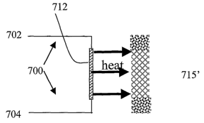
[0085] Figures 7A and 7B illustrate an exemplary phase-changing heat emitter.
The
nanofabric electrical input electrodes 702 and 704 activate electrical input
700 of
nanofabric emitting element 712 sending a current through nanofabric emitting
element
712. Nanofabric emitting element 712 having a resistance R (R is a function of
temperature and increases at high temperatures) receives electrical power
(I2R) from
electric current I and is heated to the point heat (radiation) outputs. Those
skilled in the
art will appreciate that metallic nanotubes generally dominate the
aforementioned
behavior. Heating efficiency of the nanofabric emitting element 712 is
enhanced by
reducing thermal conduction from the film to adjacent material that may act as
a heat
sink, but which changes phase. By way of example of reduced thermal
conduction, the
nanofabric emitting element 712 is that portion of the nanofabric element in a
gap (void)
region. Alternatively, nanofabric emitting element 712 is that portion of the
nanofabric
element supported by (in physical contact with) a layer of low thermal
conductivity such
as polyimide or epoxy glass, or other materials such as those previously
described.
[0086] Common materials whose phase is changed upon moderate heating include
chalcogenides such as Ge2Sb2Te5, where heating produces a phase change from
poly-
crystalline to amorphous; and such phase changes can be read and stored as
bits of
memory. The current, I, may be adjusted to control the input power I2R to
nanofabric
emitting element 712 to emit more (or less) heat (radiation) energy in order
to change the
phase of the adjacent material 715 to crystalline material 715'and back again,
as
illustrated by Figures 7A and 7B.
[0087] In general, nanotube heating elements may also be used to change the
phase of
a wide range of materials, not just chalcogenide materials. For example,
metals may have
one or more crystal structures, each of which constitutes a "phase" which may
be
selectively changed by one or more nanotube heating elements. Other materials
whose
"phase" can be changed include ceramics (structural change), glasses (above or
below
glass transition temperature), polyrners (above or below glass transition or
other transition
16
CA 02621397 2008-03-05
WO 2007/030483 PCT/US2006/034626
temperature) and silicides. It is also possible to produce other types of
phase changes
such as crystalline (poly and single) to amorphous, amorphous to crystalline
(poly and
single), above and below glass transition temperatures, between eutectoid
phases-such
as ferrite to austenite as an example-and from solid to liquid to gas.
Suspended Nanotube Heaters
[0088] Figures 8A-8D illustrate exemplary structures according to certain
embodiments of the invention. Figure 8A illustrates a single, horizontally-
suspended
heating element structure 800 having a silicon substrate 802, a source 804'
and drain 804,
a gate electrode 806, a gate dielectric 807, a first set of conductive
electrodes 808, a
chalcogenide layer 810, a nanotube fabric layer 812 and second conductive
electrodes
814.
[0089] Silicon substrate layer 802 underlies source 804' and drain 804.
Silicon
substrate layer 802 may be n-type or p-type. A gate electrode 806 is disposed
above a
gate dielectric region 807. First conductive electrodes 808 contact source
804' and drain
804. One of the first conductive electrodes 808 is in electrical communication
with
chalcogenide layer 810. A dielectric layer 813 is disposed above the first
conductive
electrode 808 what is in electrical communication with chalcogenide layer 810.
Chalcogenide layer 810 is disposed below a gap 818; gap 818 is disposed below
a
nanotube fabric (heat emitting) layer 812. In other words, gap 818 separates
chalcogenide layer 810 from nanotube layer 812. A second set of conductive
electrodes
814 contacts nanotube fabric layer 812 such that current may flow from one of
the second
electrodes 814 to the other of the second electrodes 814 through the fabric
layer 812.
[0090] An exploded view of the chalcogenide active region 809 is illustrated
in figure
8B. Heat emitted by the nanofabric 812, illustrated as the set of downward-
facing arrows
within gap 818, changes amorphous chalcogenide 810 to crystalline chalcogenide
816.
The conductive electrodes 808 and 808' are used to gauge the resistance of the
chalcogenide, and thus to deduce its phase. Control and memory
output/READ/WRITE
electrodes are not shown, but one skilled in the art will understand that they
are
interconnected within the memory system. Figure 8C illustrates a different
embodiment,
which includes ahorizontally-suspended heating element structure 817. In this
alternate
17
CA 02621397 2008-03-05
WO 2007/030483 PCT/US2006/034626
embodiment, the placement of electrodes and insulating regions is slightly
changed. As
can be seen in figure 8C, a first conductive electrode 808 contacts a lower
section of the
chalcogenide layer 810.
[0091] Figure 8D illustrates a chalcogenide memory element structure 822
having
two suspended heating elements 812. The structure 822 shares most of the same
features
as structure 800. Gaps 824 and second conductive electrodes 826 are shown. The
presence of a second heating element lends itself to advantages over a single-
element
heating systein, including increased speed of heating and redundancy within
the structure
and more uniform heating of the chalcogenide material. Since the chalcogenide
is heated
from both sides, it should be expected that the phase change rate should also
be increased,
compared to a single heater (power density on the chalcogenide is doubled).
[0092] Figure 9 illustrates an alternate embodiment of the invention having a
horizontal, suspended fabric heating element and chalcogenide layer contacted
by metal.
Structure 900 includes a silicon substrate 902, a source 904 and drain 904, a
gate
electrode 906, a gate dielectric 907 a first set of conductive electrodes 908,
a
chalcogenide layer 910, a nanotube fabric layer 912 and second conductive
electrodes
914. Structure 900 has many of the features of structure 800, illustrated in
figure 8A with
the addition of an extended metal-chalcogenide contact 908' in contact with
chalcogenide
layer 910. Therefore, nanotube fabric will heat both the metal extension 908'
and the
chalcogenide layer 910. Figure 9 is an additional design of a CRAM memory
element
that may simplify the fabrication of the memory cell.
Non-Suspended Nanotube Heaters
[0093] Figures 10A-10 E illustrate various other embodiments of the invention.
For
these figures, the in-line transistor has been eliminated from the schematics;
however, one
knowledgeable in the art understands that the lower electrodes 1008 may be
connected to
the source-drain region of a CMOS transistor or other control eleinent(s).
[0094] Figure l0A illustrates a chalcogenide memory element having two
nanotube
nanofabric heating elements 1012 and 1012' in contact with a chalcogenide
region 1010.
Lower electrode 1008 connects to nanofabric 1012; while, upper electrode 1008'
connects
to upper nanotube fabric 1012'. The nanotube fabrics 1012 and 1012' are
separated by
18
CA 02621397 2008-03-05
WO 2007/030483 PCT/US2006/034626
insulating layer 1013, which also substantially encapsulates chalcogenide
1010. Note that
nanotube fabrics 1012 and 1012' may extend beyond chalcogenide material 1010
as
shown in Figure 10A or nanofabrics 1012 and 1012' may terminate within or at
the outer
edges (away from electrodes 1008 and 1008') of chalcogenide 1010 (not shown).
[0095] This structure operates by passing a current through lower electrode
1008 and
lower nanotube fabric 1012, which produces heat and causes a phase change in
1010 and
the interface between 1012 and 1010. The state of the chalcogenide 1010 is
then probed
by passing a voltage pulse through the device from lower electrode 1008, to
nanotube
fabric 1012, chalcogenide 1010, upper nanotube fabric 1012' and upper
electrode 1008',
measuring a change in the resistance of chalcogenide 1010. Since this is a
double
nanotube heater design, the current may also be passed through upper electrode
1008' and
nanotube fabric 1012' to change the phase of the chalcogenide 1010.
[0096] Figure 10B illustrates another embodiment of a two-heating-element
chalcogenide memory element structure 1002 having many of the same elements as
structure 1000 but the fabric heating elements 1012 and 1012', chalcogenide
region 1010
and dielectric regions 1013 are disposed between conductive electrodes 1008
and 1008'.
This design does not require the creation of vias and gaps in the CRAM cell,
and thus
may be fabricated more simply than the embodiments illustrated in Figures 8A-
8D.
However, the non-suspended fabrics may not heat as readily as the suspended
fabrics due
to the loss of heat to the relatively larger substrate.
[0097] Figure 10C illustrates structure 1002, an embodiment of a chalcogenide
memory element having a single fabric heating element 1012 in contact with a
chalcogenide region 1010 having a conductive electrode 1008 and 1008' and
dielectric
regions 1013. This design includesonly one nanotube fabric 1012 to be
deposited and
patterned.
[0098] Figure 10D shows another embodiment of a non-suspended device, in
whichnanotube fabric 1012 is deposited on top of electrode 1008, which makes
contact to
additional circuitry. The nanotube fabric is also contacted to chalcogenide
material 1010
by the deposition of chalcogenide onto one end of nanotube fabric 1012. The
chalcogenide material may be completely deposited on top of the nanotube
fabric or may
19
CA 02621397 2008-03-05
WO 2007/030483 PCT/US2006/034626
be off-set so that only a small portion of the chalcogenide material is
contacting the
nanotube fabric. An over-lap of 10 nm up to the critical dimension (i.e. 150
mn for 150
nm dimensional node) of the chalcogenide is envisioned. The non-nanotube
contacted
edge of chalcogenide 1010 is further connected to conductive electrode 1008'.
This
simplified design operates by passing a current through nanotube heating
fabric 1012 by
route of electrode 1008. The heating of nanotube fabric 1012 causes the phase
of
chalcogenide 1010 to change from a crystalline phase to an amorphous phase (as
seen in
Figure 8). After changing the phase of chalcogenide 1010, a smaller probe
voltage is
applied through electrode 1008, nanotube fabric 1012, chalcogenide 1010 and
electrode
1008' to sense the high resistance state of chalcogenide 1010.
[0099] Figure l0E shows another embodiment, which is similar to Figure 10D
except
that nanotube fabric 1012 is deposited on top of chalcogenide 1010 with
nanotube over-
lapping region 1012' (region where nanotube is deposited on top of
chalcogenide 1010),
changing the heating profile of chalcogenide 1010 compared to Figure 10D.
Electrode
1008' maybe deposited below (as shown) or on top of chalcogenide 1010 (not
shown). If
electrode 1008' is deposited on top of chalcogenide 1010, then care must be
taken that
nanotube fabric 1012' does not contact electrode 1008'.
Vertically Disposed Suspended Nanotube Heaters
[0100] Figures 11A-11D illustrate embodiments of chalcogenide memory elements
having vertically disposed fabric heating elements. Figures 11A-B show non-
suspended
vertical devices while figures 11 C-D show suspended vertical devices.
[0101] Structure 1100 has silicon substrate layer 1102, source 1104' and drain
1104,
gate 1106, gate dielectric 1107, first conductive (or lower) electrode 1108,
upper
conductive electrode 1108', insulator region 1113, vertically-aligned nanotube
heating
element 1112, chalcogenide region 1110, and second conductive electrodes 1114
as
illustrated in figure 11A. Fabrication of such vertically disposed fabric
layers is fully
described in the incorporated patent references and is not repeated here for
the sake of
brevity.
[0102] Figure 11 B illustrates structure 1117, a chalcogenide memory element
having
two fabric heating elements 1112 and 1112' in contact with a chalcogenide
region 1110.
CA 02621397 2008-03-05
WO 2007/030483 PCT/US2006/034626
Many of the elements in structure 1100 are the same as the elements in
structure 1117,
with the addition of the second heating element (1112'), dielectric regions
1113 insulating
the heating elements from conductive electrodes 1108 and 1108'.
[0103] Figures 11 C and 11 D illustrate chalcogenide memory elements having
suspended, vertically aligned heating elements. Structure 1118 has a gap 1120
separating
fabric heating element 1112 from chalcogenide region 1110, as illustrated in
figure 11 C.
One skilled in the art will understand how to fabricate such suspended regions
as these
elements are analogous to those elements described in incorporated references,
see, e.g.
U.S. Pat. Appl. No. 10/776,572 entitled "Devices Having Vertically-Disposed
Nanofabric
Articles and Methods of Making the Same", filed Feb. 11, 2004. Figure 11D
illustrates
structure 1119 having two fabric heating elements 1112 and 1112' separated
from
chalcogenide region 1110 by gaps 1120 and 1120' and spaced by dielectric
layers 1113
and 1113'.
[0104] Figures 12A-12B show other embodiments of vertically-oriented nanotube
heaters used to change the phase of chalcogenide material. In Figure 12A, the
vertical
nanofabric 1212 contacts one side of the chalcogenide material 1210, while in
Figure
12B, the nanotube fabric 1212 only contacts a minimum amount of chalcogenide
1210 on
the order of the thickness of the nanotube fabric (minimum of 1.5 nm maximum
of
several tens of nanometers for multilayered fabric). The width of the fabric
(dimension
into the page) is tailored through the patterning of the vertically oriented
fabric with a
minimum of several nanometers and a maximum of several microns possible.
Similar to
previous design 1208 and 1208' are upper and lower electrodes, respectively
and 1213 is
an insulating layer.
[0105] Devices such as heat emitting filaments can be constructed using
nanofabrics
that conform to a surface which is substantially perpendicular to a
semiconductor
substrate (i.e., "vertically-oriented"), and that such devices can be used as
vertically
oriented switches in a plethora of applications. Fabrication techniques to
develop such
horizontally- and vertically-disposed fabrics and devices composed of nanotube
fabrics
which comprise redundant conducting nanotubes may be created via CVD, or by
room
temperature operations as described herein and described in the incorporated
patent
references. Such fabrication techniques include the ability to form said
suspended heat
21
CA 02621397 2008-03-05
WO 2007/030483 PCT/US2006/034626
emitters for use in many different articles having relatively short spans of
suspended
nanofabric articles. In some embodiments, this allows smaller device
dimensions and
higher strains in the nanofabric articles, as well as lower electrical
resistances. Such
articles may be adapted or modified to perform function within the electronics
industry
such as heat or heat emission or be part of a scheme involving transmission or
storage
functionality.
[0106] In another embodiment, the heating element is disposed adjacent to or
contacting a material, which need not have crystallizing behavior but could be
a
conductor, insulator or have some other property that is affected by the
transfer of heat.
[0107] Figures 13A-13B show another embodiment of this invention where an
initially amorphous chalcogenide material 1311 is employed rather than an
initially
crystalline chalcogenide 1310. For this device, structure 1300 shows a
nanotube fabric
1312, which shows a fabric with individual nanotubes, deposited on top of a
lower
electrode 1308 and insulator 1313. Instead of crystalline chalcogenide
material,
amorphous chalcogenide material 1311 is then deposited on top of nanotubes
1312. A
crystalline chalcogenide material 1310 is then deposited on top of the
amorphous
chalcogenide 1311 followed by an upper electrode 1308'. It is also possible to
remove
the crystalline chalcogenide layer 1310 and have the upper electrode 1308'
deposited
directly on top of amorphous chalcogenide layer 1311.
[0108] Figure 13B shows the operation of this device in that as the nanotube
fabric is
heated, conductive channels 1310' are formed around the nanotubes, bridging
the
conductive nanotubes to the crystalline chalcogenide 1310 or upper electrode
1308'.
Other designs, e.g., designs similar to those presented in Figures 8A-8D, 9,
10A-10E,
11A-11D, and -12A-12B, are also possible. In this embodiment, the chalcogenide
device
is normally in the high resistance position and thinner chalcogenide layers
would be
required as long as a conductive channel can be formed to the upper electrode.
It may be
possible to deposit a thin layer of amorphous chalcogenide of the same order
of thickness
as the nanotube fabric to make this type of device.
[0109] Although the main route for probing the change of phase for a
chalcogenide
device such as those presented in Figures 8-13 is by the measuring of a
resistance change,
22
CA 02621397 2008-03-05
WO 2007/030483 PCT/US2006/034626
the inventors also envision the ability to measure a phase change in the
chalcogenide
material by measuring a change in wavelength of a laser that is impinged on
the
chalcogenide material. This technique is readily known in the art and is
similar to the
operation of CD-RWs and recordable DVDs.
[0110] Figure 14 illustrates a nanotube apparatus 1400 under another
embodiment of
the nanotube heating element. A drive circuit 1401 controls the application of
electrical
stimulus to the nanotube element. Dependent upon the particular application,
the drive
circuit is capable of providing a predefined current through contact
electrodes to the
nanotube element. In a preferred embodiment, the nanotube element 1402 is a
heat-
emitting portion of nanotube fabric of a predefined geometry. The current from
the drive
circuit controls the amount of heat emitted from the nanotube element and the
time period
over which heat is emitted. Element 1403 is an article to be heated by the
nanotube
element positioned in proximity to nanotube element 1402. In a preferred
embodiment
the article is a material capable of changing its physical state in response
to temperature
changes. The application of heat by the nanotube element induces in the
article a
predetermined temperature change capable of inducing a phase change in the
article.
[0111] As is described above, the nanotube apparatus may be used, in preferred
embodiments, as a CRAM circuit. For CRAM applications, the article to be
heated 1403
is a chalcogenide material in which phase change correlates with a change of
memory
state. By varying the geometry of the nanotube element 1402 and the electrical
stimulus
applied to it by the drive circuit 1401, the amount of heat emitted by the
nanotube
element can be adjusted to suit the various applications. The electrical
stimulus applied
by the drive circuit 1401 to control heat emission from the nanotube element
1402 is
determined from variables including: resistance of the nanotube element,
resistance of the
contact electrodes, whether the nanotube element is in direct contact with the
article to be
heated or suspended over a gap, and the electrical and thermal properties of
supporting
structure materials. As described above, it was found that temperature changes
of, e.g.,
several hundred Kelvin in the nanotube element can be induced on a very short
timescale
(e.g., down to sub-picosecond) by passing through the nanotube element very
small
currents (e.g., less than about 100 A). This method of emitting heat from a
nanotube
element provided in Figure 14 may be useful in CRAM applications.
23
CA 02621397 2008-03-05
WO 2007/030483 PCT/US2006/034626
[0112] The following commonly-owned patent references, referred to herein as
"incorporated patent references," describe various techniques for creating
nanotube
elements (nanotube fabric articles, which may be used asheat emitters), e.g.,
creating and
patterning nanotube fabrics, and are incorporated herein by reference in their
entireties:
U.S. Patent Application No. 09/915,093, Electromechanical Memory Array Using
Nanotube Ribbons and Method for Making Same, filed July 25, 2001, now U.S.
Pat. NO. 6,919,592;
U.S. Patent Application No. 09/915,095, Hybrid Circuit Having Nanotube
Electromechanical Memory, filed July 25, 2001, now U.S. Patent No. 6,574,130;
U.S. Patent Application No. 09/915,173, Electromechanical Memory Having Cell
Selection Circuitry Constructed with Nanotube Technology, filed July 25, 2001,
now U.S. Patent No. 6,643,165;
U.S. Patent Application No. 10/03 3,032, Methods ofMaking Electromechanical
Three-Trace Junction Devices, filed December 28, 2001, now U.S. Patent No.
6,784,028;
U.S. Patent Application No. 10/033,323, Electromechanical Tlaree-Trace
Junction
Devices, filed December 28, 2001 now U.S. Patentb No. 6,911,682;
U.S. Patent Application No. 10/128,117, Methods ofNanotube Films andArticles,
filed April 23, 2002, now U.S. Patent No. 6,835,591;
U.S. Patent Application No. 10/128,118, Nanotube Films and Articles, filed
April
23, 2002, now U.S. Patent No. 6,706,402;
U.S. Patent Application No. 10/341,005, Methods of Making Carbon Nanotube
Films, Layers, Fabrics, Ribbons, Elements and Articles, filed on January 13,
2003;
U.S. Patent Application No. 10/341,054, Methods of Using Pre formed Nanotubes
to Make Carbon Nanotube Films, Layers, Fabrics, Ribbons, Elements and
Articles, filed January 13, 2003;
24
CA 02621397 2008-03-05
WO 2007/030483 PCT/US2006/034626
U.S. Patent Application No. 10/341,055, Methods of Using Thin Metal Layers to
Make Carbon Nanotube Films, Layers, Fabrics, Ribbons, Elements and Articles,
filed January 13, 2003;
U.S. Pat. Application No. 10/341,130, Carbon Nanotube Films, Layers, Fabrics,
Ribbons, Elements and Articles, filed January 13, 2003;
U.S. Patent Application No. 10/776,059, Electromechanical Switches and
Memory Cells Using Horizontally-Disposed Nanofabric Articles and Methods of
Making Same, filed February 11, 2004;
U.S. Patent Application No. 10/776,572, Electromechanical Switches and
Memoyy Cells Using Vertically-Disposed Nanofabric Articles and Methods of
Making the Same, filed February 11, 2004, now U.S. Pat. No. 6,924,538;
U.S. Patent Application No. 10/936119, Patterning of Nanoscopic Articles and
Methods of Making Same, filed on Sep. 8, 2003, now Publication No.
2005/0128788; and
W.O. No. 01/03,208, Nanoscopic Wire-Based Devices, Arrays and Metlaods of
Tlaeir Manufacture, filed Jan. 11, 2001 now Publication No. US0018138.
[0113] It will be further appreciated that the scope of the present invention
is not
limited to the above-described embodiments but rather is defined by the
appended claims,
and that these claims will encompass modifications of and improvements to what
has
been described.
[0114] What is claimed is: