Note: Descriptions are shown in the official language in which they were submitted.
CA 02621411 2008-03-05
1
DESCRIPTION
ADHESIVE STRUCTURE AND MANUFACTURING METHOD THEREOF
TECHNICAL FIELD
[00011
The present invention relates to an adhesive structure and a
manufacturing method thereof. More specifically, the present invention relates
to an adhesive structure that forms a minute structure on a surface of a base
thereof, thus being capable of adhering onto an adhesion target without using
welding, an adhesive, or the like, and relates to a manufacturing method of
the
adhesive structure.
BACKGROUND ART
[0002]
Heretofore, adhesion using welding or an adhesive, adhesion using an
interposed fastening member such as a hook-and-loop fastener and a bolt, and
the
like have been employed in adhesion of materials.
DISCLOSURE OF INVENTION
[0003]
However, in manufacturing processes of these adhesive structures, for
example, there have existed adhesive materials such as the bolt, the
hook-and-loop fastener body and the adhesive, and fastening apparatuses such
as
a tooling machine for fastening the bolt, an adhesive coating machine and a
spot
welding machine, and accordingly, there have been various problems owing to
restrictions caused therefrom. For example, in the welding, the welding
apparatus and a spark prevention measure have been required, and in the
adhesive,
a countermeasure has been required, which is against a work environment where
a solvent volatilizes and adheres onto clothes of a worker. Moreover, also in
the
CA 02621411 2008-03-05
2
case of the adhesion by the hook-and-loop fastener, the adhesive has been used
for fixing the hook-and-loop fastener itself to an adhesion target.
[0004]
In order to solve these problems, such a countermeasure of changing the
adhesive to a non-solvent adhesive of a hot-melt type has been taken in the
field
of the environment; however, as steps, there have been a coating step and a
heating step, and accordingly, there have been problems such as an increase of
working hours and an increase of cost. Moreover, also in the welding, friction
welding and the like have been developed; however, even in this case,
development and introduction of new equipment have been required, which has
not leaded to reduction of the hours required for the steps and reduction of
the
cost.
[0005]
Meanwhile, there have been proposed a functional board and a functional
device, which include a group of minute protrusions of organic polymer, and
proposed a microbiochip and an optical device, which use these minute
protrusions (refer to Japanese Patent Unexamined Publication No. 2004-170935).
[0006]
The present invention has been made in order to solve the
above-described problems. It is an object of the present invention to provide
an
adhesive structure capable of adhering onto the adhesion target without
requiring
the adhesive materials or the adhesion apparatuses, such as the welding and
the
adhesive, and to provide a manufacturing method of the adhesive structure.
[0007]
An adhesive structure according to a first aspect of the present invention
includes: a base; and a plurality of protrusions, in which tip ends are
spherical
with a radius of 300 nm or less, and a radius of cross sections perpendicular
to a
longitudinal direction is 300 nm or less, the protrusions being provided on a
surface of the base.
[0008]
CA 02621411 2008-03-05
3
A method of manufacturing an adhesive structure according to a second
aspect of the present invention includes the steps of: forming protrusions, in
which tip ends are spherical with a radius of 300 nm or less, and a radius of
cross
sections perpendicular to a longitudinal direction is 300 nm or less; and
providing
the protrusions on a surface of a base.
BRIEF DESCRIPTION OF THE DRAWINGS
[0009]
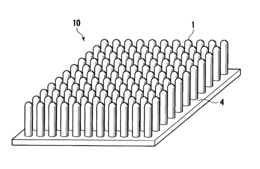
[fig. 1] FIG. 1 is a perspective view showing an example of an adhesive
structure
of the present invention.
[fig. 2] FIG. 2 is a schematic view explaining van der Waals force.
[fig. 3] FIG. 3 is a schematic view showing a mechanism where the adhesive
structure of the present invention exerts adhesive force.
[fig. 4] FIG. 4 is a schematic cross-sectional view showing examples of tip
ends
of protrusions.
[fig. 5] FIG. 5 is a graph showing a relationship between a radius of the tip
ends
of the protrusions and the adhesive force.
[fig. 6] FIG. 6 is a cross-sectional view showing other examples of the
adhesive
structure of the present invention.
[fig. 7] FIG. 7 is a schematic view showing steps of a nanoimprinting method.
[fig. 8] FIG. 8 is a schematic view showing a process of a UV curing method.
[fig. 9] FIG. 9 is a table showing evaluation conditions and evaluation
results of
examples and a comparative example.
[fig. 10] FIG. 10 is a graph showing relationships between the radii of the
tip ends
and the adhesive forces in a case where the protrusions are made of
polystyrene.
[fig. 11 ] FIG. 11 is a graph showing relationships between the radii of the
tip ends
and the adhesive forces in a case where the protrusions are made of 6-Nylon.
[fig. 12] FIG. 12 is a graph showing relationships between the radii of the
tip ends
and the adhesive forces in a case where the protrusions are made of
polypropylene.
CA 02621411 2008-03-05
4
BEST MODE FOR CARRYING OUT THE INVENTION
[0010]
A description will be made below in detail of embodiments of an
adhesive structure of the present invention and a manufacturing method thereof
based on the drawings.
[00111
As shown in FIG. 1, in an adhesive structure 10 of the present invention,
a plurality of protrusions 1 are provided on a surface of a base 4. Then, the
protrusions 1 have a columnar structure in which a radius of cross sections
perpendicular to a longitudinal direction is 500 nm or less. In such a way, by
using van der Waals force acting between the protrusions 1 and an adhesion
target
2, materials can be adhered onto each other without requiring an adhesive
member such as an adhesive or an apparatus for executing the adhesion.
[0012]
Specifically, as shown in FIG. 2, van der Waals force represented by the
following general expression (1) acts among atoms.
[0013]
F oc AlD2 (1)
In the expression (1), algebraic symbol A indicates a constant depending
on a dielectric constant of a material of the protrusions, and algebraic
symbol D
indicates a nearest distance between the protrusions 1 and the adhesion target
2.
[0014]
As shown in FIG. 3, the adhesive structure 10 of the present invention
includes the plurality of protrusions 1 of a nanometer level, and accordingly,
in
comparison with a protrusion 6 of a micrometer level, the protrusions 1 enter
irregularities of a surface of the adhesion target 2 by the nanometer level,
and can
exert strong adhesive force. Note that, in order to exert such adhesive force,
it
is necessary that the protrusions 1 and the adhesion target 2 come close to
each
other at an interatomic bond distance between atoms composing the protrusions
1
CA 02621411 2008-03-05
and atoms composing the adhesion target 2.
[0015]
The protrusions 1 in the adhesive structure 10 of the present invention
have the columnar structure in which the radius of the cross sections of the
protrusions 1, which are perpendicular to the longitudinal direction thereof,
is
500 nm or less. When the radius of the protrusions exceeds 500 nm, the
protrusions 1 are hindered from entering the minute irregularities of the
surface
of the adhesion target 2, and the van der Waals force comes not to act
therebetween. Meanwhile, when the radius is less than 50 nm, the adjacent
protrusions 1 sometimes stick to one another. Hence, the radius of the cross
sections of the protrusions 1 is preferably within a range of 50 to 500 nm,
more
preferably, 50 to 300 nm inclusive.
[0016]
Here, as shown in (a) to (d) of FIG. 4, each of the protrusions 1 can be
formed into a variety of shapes. Specifically, the entirety of the protrusion
may
be columnar as shown in (a), or the protrusion may be semispherical as shown
in
(b). Moreover, only a tip end of the columnar protrusion may be semispherical
as shown in (c), or the tip end of the protrusion may be spherical as shown in
(d).
Among them, it is particularly preferable that the shape of the tip end
portion of
the protrusion 1 be spherical. By the fact that the shape of the tip end is
spherical, it becomes easier for the protrusions to enter the minute irregular
structure of such an adhesion target surface, thus making it possible to
generate
strong van der Waals force between the protrusions and the adhesion target.
Note that, when the shape of the tip ends of the protrusions is spherical or
semispherical, that is, when the tip ends of the protrusions are spherical, it
is
preferable that a radius (curvature radius) R of spheres be 300 nm or less.
Moreover, it is preferable that the radius R of the spheres be within a range
of 50
to 300 nm based on a relationship thereof with the radius of the cross
sections of
the protrusions 1. Note that, in this specification, the term "spherical"
incorporates not only the spherical shape but also an oval shape or a shape
similar
CA 02621411 2008-03-05
6
thereto.
[0017]
Moreover, as shown in FIG. 3, the protrusions 1 may have a shape in
which such a cross-sectional radius is gradually decreased from base portions
to
the tip end portions. However, also in this case, it is preferable that the
tip ends
of the protrusions be spherical or semispherical.
[0018]
FIG. 5 shows a relationship between such a tip end radius of the
protrusions and the adhesive force. In the conventional hook-and-loop
fastener,
adhesion strength thereof is approximately 20 to 40 N/cm2. Meanwhile, in this
embodiment, as a graph in FIG. 5 shows, stronger adhesive force than
heretofore
can be obtained if the tip end radius R of the protrusions is 300 nm or less.
[0019]
Note that a shape of the cross sections of the protrusions 1, which are
with respect to the longitudinal direction thereof, is preferably circular;
however,
without being limited to this, the shape may be polygonal such as tetragonal
and
pentagonal.
[0020]
Moreover, it is preferable that the above-described protrusions be made
of a material with a dielectric constant of 2 or more (ASTMD 150, @ 1 MHz,
20 C). When the dielectric constant is less than 2, the van der Waals force
acting on the tip ends of the protrusions is not sufficient, and the adhesion
strength is prone to be insufficient.
[0021]
Furthermore, from a viewpoint of controlling the dielectric constant of
the material, it is preferable that the protrusions be made of a composite
material
containing a conductive substance. As such a conductive substance, there can
be mentioned: a carbon raw material such as carbon black, graphite, black lead
and carbon nanotube; particles of metal such as copper, silver and nickel;
indium
tin oxide; titanium oxide; metal fiber such as stainless steel fiber; and the
like.
CA 02621411 2008-03-05
7
[0022]
Still further, it is preferable that the material of the above-described
protrusions be resin. In the case where the protrusions are composed of the
resin, when the protrusions contact the surface of the adhesion target, the
protrusions are deformed owing to flexibility/collapsibility of the resin,
whereby
the number of contacts with the minute irregularities of the surface of the
adhesion target is increased, thus making it possible to further ensure the
adhesion strength. As the resin composing the protrusions, there can be
suitably
used: acrylic resin such as polymethacrylate and polyacrylate; polyamide resin
such as 6-Nylon and 6,6-Nylon; polyolefin resin such as polystyrene,
polyethylene and polypropylene; polyvinyl chloride; polyurethane;
polycarbonate; polyacetal; polytetrafluoroethylene; and the like. Moreover, a
composite resin material such as a particle reinforced one, a fiber reinforced
one
and a mineral reinforced one can also be suitably used.
[0023]
Moreover, from a viewpoint of the flexibility/collapsibility of the
protrusions, it is preferable that a bending elastic modulus of the
protrusions be 5
GPa or less. When the bending elastic modulus exceeds 5 GPa, it becomes
difficult to ensure the flexibility for allowing the protrusions to follow the
shape
of the minute irregularities of the adhesion target.
[0024]
Furthermore, it is more preferable that the resin composing the
above-described protrusions be a material of which dielectric constant and
bending elastic modulus belong to the above-described ranges.
[0025]
Moreover, it is preferable that an aspect ratio of the above-described
protrusions be within a range of 1 to 15. When the aspect ratio is less than
1, it
becomes difficult for the protrusions to follow the adhesion target, and the
entire
adhesion strength becomes prone to be decreased. When the aspect ratio
exceeds 15, the protrusions are sometimes broken by a pressing pressure. It is
CA 02621411 2008-03-05
8
more preferable that the aspect ratio be within a range of 1 to 4. In this
case, the
protrusions are less likely to collapse at the time of manufacture thereof,
and a
yield thereof can be improved. Note that, in this specification, as shown in
FIG.
4(a), the aspect ratio is a value obtained by dividing a length L of each
protrusion
by a cross-sectional diameter D thereof. Moreover, the cross-sectional
diameter
D is a cross-sectional diameter of the protrusion at a midpoint of the length
L.
[0026]
In the adhesive structure of the present invention, it is possible to coat,
on the above-described protrusions, a thin film with a thickness of 300 nm or
less.
Specifically, as shown in FIG. 4(e), a thin film 3 can be formed on the
entirety of
each protrusion 1. In this case, when the thickness of the thin film exceeds
300
nm, the tip end radius of the protrusions becomes too large, and the
protrusions
cannot enter the minute irregularities of the surface of the adhesion target,
and
the van der Waals force is prone to be hindered from being exerted. Like the
above-described protrusions, it is preferable that a material composing the
thin
film has a dielectric constant of 2 or more. Moreover, in a similar way, it is
preferable that the material composing the thin film be a composite material
composed by being added with the resin and the conductive substance like the
above-described protrusions.
[0027]
Note that the protrusions may have a hollow shape formed of only the
thin film. Typically, it is possible to form such a thin film by chemical
vapor
deposition (CVD) and physical vapor deposition (PVD), which use a vacuum
state, a plasma state and the like, dipping into a solution, and the like.
[0028]
Moreover, while the adhesive structure of the present invention is
composed by forming the plurality of minute protrusions 1 on the base 4 as
shown in FIG. 1, it is preferable that such protrusions be provided in such a
high
density of approximately 106 to 1011 pieces per 1 cmZ of the base.
[0029]
CA 02621411 2008-03-05
9
Furthermore, the adhesive structure of the present invention can be
provided with a distribution of the adhesion strength. For example, the
protrusions are arrayed while setting a distance among the protrusions at an
unequal pitch, thus making it possible to easily peel the adhesive structure
from
the adhesion target in the case of reusing or tearing down the adhesive
structure
firmly adhered thereonto. Moreover, it is possible to set the unequal pitch of
the
protrusions freely in any of lengthwise, crosswise and oblique directions.
Furthermore, it is also possible to set such an inter-protrusion distance for
each of
the protrusions or for each of units, each of which is formed by combining an
arbitrary number of the protrusions.
[0030]
Moreover, it is possible to form the protrusions integrally with the
surface of the base by a transcription method, an injection molding method,
and
the like. These methods enable the protrusions to be formed also on a surface
of
the composite resin material. In the resin material into which a reinforcement
material (filler) is mixed, in general, the reinforcement material is not
exposed to
the surface of the resin material, but is covered with a resin layer.
Accordingly,
a resin component of the surface is softened and molded, whereby the
protrusions
composed only of the resin component can be obtained.
[0031]
In the adhesive structure of the present invention, the same material as
that of the protrusions 1 can be used as the base 4 on which the protrusions 1
are
formed. Besides the above, a variety of materials can be appropriately
selected
and used according to purposes. For example, a metal oxide such as alumina,
resin such as polyimide resin and epoxy resin, metals such as aluminum,
silicon,
iron, titanium and magnesium, glass, and the like can be used.
[0032]
Moreover, the hook-and-loop fastener can also be obtained by using the
adhesive structure of the present invention. Specifically, in two of the
adhesive
structures, surfaces thereof on which the protrusions are formed are contacted
CA 02621411 2008-03-05
with each other, whereby the hook-and-loop fastener can be obtained. The
surfaces of the adhesive structures, on which the protrusions are formed, are
contacted with each other, whereby the van der Waals force acts between the
protrusions, and the adhesive structures can be firmly adhered onto each
other.
[0033]
Next, a description will be made of the manufacturing method of the
adhesive structure of the present invention.
[0034]
In the manufacturing method of the present invention, the protrusions 1
and the base 4 are integrally formed by the transcription method, whereby the
above-described adhesive structure is obtained. For example, it is possible to
form the protrusions by so-called stamp molding of heating the base, thrusting
a
molding die against the base, and flowing the resin therein (refer to FIG.
6(a)).
[0035]
Moreover, in another manufacturing method of the present invention, the
protrusions 1 and a base 5 are formed separately from each other, and then the
protrusions 1 and the base 5 are integrated with each other, whereby the
above-described adhesive structure can be obtained. Specifically, after the
protrusions 1 are formed on a film or the like in advance, the protrusions 1
are
integrated with the base 5 made of the glass, the metal, the ceramics, the
resin or
the like, whereby the adhesive structure can be obtained (refer to FIG. 6(b)).
Moreover, the protrusions 1 fabricated separately are embedded onto a surface
of
the base 5, thus also making it possible to form the adhesive structure (refer
to
FIG. 6(c)).
[0036]
Here, the transcription method (nanoimprinting method) is a method
capable of producing ultraprecise resin surfaces in quantity at low cost by a
molding die processed minutely to a nanometer size. As the die (stamper) for
use, there are dies in which grooves are formed on silicon, ceramics (SiC) and
the
like by an electron beam lithography method, metal dies formed by inversion of
CA 02621411 2008-03-05
11
these by electroforming, and the like. Moreover, as the transcription method,
there are a heating type (hot-emboss method), an ultraviolet curing type (UV
curing method), and the like.
[0037]
FIG. 7 shows a nanoimprinting process by the hot-emboss method.
First, the base 4 made of the resin or the like is heated up to a glass
transition
temperature (FIG. 7(a)), and thereafter, a molding die 7 processed minutely is
thrust against the base 4 (FIG 7(b)). Then, the base 4 is cooled while the
molding die 7 is keeping on being thrust thereagainst, and the molding die 7
is
released therefrom, thus making it possible to obtain the adhesive structure
on
which the protrusions 1 of the nanometer size are formed (FIG. 7(c)).
[0038]
FIG. 8 shows a nanoimprinting process by the UV curing method. In
the UV curing method, a transparent substance such as quartz is used as the
mold.
Specifically, as shown in FIG. 8, a molding die 8 is thrust against the base 4
made
of ultraviolet curing resin, thereafter, an ultraviolet ray is irradiated onto
the base
through the mold, whereby the resin is cured, and the molding die 8 is
released
from the base, thus making it possible to obtain the adhesive structure on
which
the protrusions 1 of the nanometer size are formed.
[0039]
The present invention will be described below more in detail by
examples and a comparative example; however, the present invention is not
limited to these examples.
[0040]
(Evaluation Method)
In each of the examples, the adhesive force and the dielectric constant
were measured by the following methods.
[0041]
<Adhesive Force>
Glass, iron plates, silicon wafers were used as the adhesion targets.
CA 02621411 2008-03-05
12
Each of the adhesion targets was mounted on the surface having the
protrusions,
and a load of 100 g was applied thereto, and the adhesion target and the
surface
were left standing for 30 minutes. Thereafter, the adhesion strength was
measured by tensile strength.
[0042]
<Dielectric Constant>
The dielectric constant was measured in conformity with ASTMD 150.
Measurement conditions were set at 1 MHz and 20 C.
[0043]
(Example 1)
Polystyrene films (PS films; dielectric constant: 2.5) with a thickness of
200 m were fabricated by a spin casting method. Thereafter, on a surface of
each of the films, a sample with an area of 5 mm square was fabricated by the
nanoimprinting method. On the sample, columnar protrusions with a tip end
radius of 90 nm and a length of 1.2 m were arrayed at an interval of 180 nm.
[0044]
When the adhesive forces were measured by using these samples, the
adhesion strengths became 43.1 N/cm2 in the glass, 68.1 N/cm2 in the iron
plate,
and 74.7 N/cm2 in the silicon wafer.
[0045]
(Example 2)
Polystyrene films (dielectric constant: 2.5) with a thickness of 200 m
were fabricated by the spin casting method. Thereafter, on a surface of each
of
the films, a sample with an area of 5 mm square was fabricated by the
nanoimprinting method. On the sample, columnar protrusions with a tip end
radius of 125 nm and a length of 1.2 m were arrayed at an interval of 250 nm.
[0046]
When the adhesive forces were measured by using these samples, the
adhesion strengths became 31.0 N/cm2 in the glass, 49.0 N/cm2 in the iron
plate,
and 53.8 N/cm2 in the silicon wafer.
CA 02621411 2008-03-05
13
[0047]
(Example 3)
Polystyrene films (dielectric constant: 2.5) with a thickness of 200 m
were fabricated by the spin casting method. Thereafter, on a surface of each
of
the films, a sample with an area of 5 mm square was fabricated by the
nanoimprinting method. On the sample, columnar protrusions with a tip end
radius of 250 nm and a length of 1.2 m were arrayed at an interval of 500 nm.
[0048]
When the adhesive forces were measured by using these samples, the
adhesion strengths became 15.6 N/cm2 in the glass, 24.5 N/cm2 in the iron
plate,
and 26.9 N/cm2 in the silicon wafer.
[0049]
(Example 4)
Polystyrene films (dielectric constant: 2.5) with a thickness of 200 m
were fabricated by the spin casting method. Thereafter, on a surface of each
of
the films, a sample with an area of 5 mm square was fabricated by the
nanoimprinting method. On the sample, columnar protrusions with a tip end
radius of 90 nm and a length of 1.2 m were arrayed at an interval of 270 nm.
[0050]
When the adhesive forces were measured by using these samples, the
adhesion strengths became 19.2 N/cm2 in the glass, 30.2 N/cm2 in the iron
plate,
and 33.3 N/cm2 in the silicon wafer.
[00511
(Example 5)
Polystyrene films (dielectric constant: 2.5) with a thickness of 200 m
were fabricated by the spin casting method. Thereafter, on a surface of each
of
the films, a sample with an area of 5 mm square was fabricated by the
nanoimprinting method. On the sample, columnar protrusions with a tip end
radius of 90 nm and a length of 1.2 m were arrayed at an interval of 360 nm.
[0052]
CA 02621411 2008-03-05
14
When the adhesive forces were measured by using these samples, the
adhesion strengths became 10.8 N/cm2 in the glass, 17.0 N/cm2 in the iron
plate,
and 18.7 N/cm2 in the silicon wafer.
[0053]
(Example 6)
Polytetrafluoroethylene films (PTFE films; dielectric constant: 2.1) with
a thickness of 200 m were fabricated by the spin casting method. Thereafter,
on a surface of each of the films, a sample with an area of 5 mm square was
fabricated by the nanoimprinting method. On the sample, columnar protrusions
with a tip end radius of 90 nm and a length of 1.2 m were arrayed at an
interval
of 180 nm.
[0054]
When the adhesive forces were measured by using these samples, the
adhesion strengths became 33.2 N/cm2 in the glass, 52.3 N/cm2 in the iron
plate,
and 57.4 N/cm2 in the silicon wafer.
[0055]
(Example 7)
6-Nylon films (PA6 films; dielectric constant: 3.3) with a thickness of
200 m were fabricated by the spin casting method. Thereafter, on a surface of
each of the films, a sample with an area of 5 mm square was fabricated by the
nanoimprinting method. On the sample, columnar protrusions with a tip end
radius of 90 nm and a length of 1.2 m were arrayed at an interval of 180 nm.
[0056]
When the adhesive forces were measured by using these samples, the
adhesion strengths became 66.0 N/cm2 in the glass, 103.9 N/cm2 in the iron
plate,
and 114.2 N/cm2 in the silicon wafer.
[0057]
(Example 8)
6-Nylon films (dielectric constant: 3.3) with a thickness of 200 m were
fabricated by the spin casting method. Thereafter, on a surface of each of the
CA 02621411 2008-03-05
films, a sample with an area of 5 mm square was fabricated by the
nanoimprinting method. On the sample, columnar protrusions with a tip end
radius of 90 nm and a length of 1.2 m were arrayed at an interval of 270 nm.
[0058]
When the adhesive forces were measured by using these samples, the
adhesion strengths became 25.6 N/cm2 in the glass, 46.2 N/cm2 in the iron
plate,
and 50.7 N/cm2 in the silicon wafer.
[0059]
(Example 9)
6-Nylon films (dielectric constant: 3.3) with a thickness of 200 m were
fabricated by the spin casting method. Thereafter, on a surface of each of the
films, a sample with an area of 5 mm square was fabricated by the
nanoimprinting method. On the sample, columnar protrusions with a tip end
radius of 90 nm and a length of 1.2 m were arrayed at an interval of 360 nm.
[0060]
When the adhesive forces were measured by using these samples, the
adhesion strengths became 14.4 N/cm2 in the glass, 26.0 N/cm2 in the iron
plate,
and 28.5 N/cm2 in the silicon wafer.
[0061]
(Example 10)
Vinyl chloride films (dielectric constant: 3.2) with a thickness of 200 m
were fabricated by the spin casting method. Thereafter, on a surface of each
of
the films, a sample with an area of 5 mm square was fabricated by the
nanoimprinting method. On the sample, columnar protrusions with a tip end
radius of 90 nm and a length of 1.2 m were arrayed at an interval of 180 nm.
[0062]
When the adhesive forces were measured by using these samples, the
adhesion strengths became 46.4 N/cm2 in the glass, 73.0 N/cm2 in the iron
plate,
and 80.3 N/cm2 in the silicon wafer.
[0063]
CA 02621411 2008-03-05
= 16
(Example 11)
Polypropylene films (PP films; dielectric constant: 2.3) with a thickness
of 200 m were fabricated by the spin casting method. Thereafter, on a surface
of each of the films, a sample with an area of 5 mm square was fabricated by
the
nanoimprinting method. On the sample, columnar protrusions with a tip end
radius of 90 nm and a length of 1.2 m were arrayed at an interval of 180 nm.
[0064]
When the adhesive forces were measured by using these samples, the
adhesion strengths became 43.5 N/cm2 in the glass, 68.5 N/cm2 in the iron
plate,
and 75.3 N/cm2 in the silicon wafer.
[0065]
(Example 12)
Polypropylene films (dielectric constant: 2.3) with a thickness of 200 m
were fabricated by the spin casting method. Thereafter, on a surface of each
of
the films, a sample with an area of 5 mm square was fabricated by the
nanoimprinting method. On the sample, columnar protrusions with a tip end
radius of 90 nm and a length of 1.2 m were arrayed at an interval of 270 nm.
[0066]
When the adhesive forces were measured by using these samples, the
adhesion strengths became 16.9 N/cm2 in the glass, 30.5 N/cm2 in the iron
plate,
and 33.5 N/cm2 in the silicon wafer.
[0067]
(Example 13)
Polypropylene films (dielectric constant: 2.3) with a thickness of 200 m
were fabricated by the spin casting method. Thereafter, on a surface of each
of
the films, a sample with an area of 5 mm square was fabricated by the
nanoimprinting method. On the sample, columnar protrusions with a tip end
radius of 90 nm and a length of 1.2 m were arrayed at an interval of 360 nm.
[0068]
When the adhesive forces were measured by using these samples, the
CA 02621411 2008-03-05
= 17
adhesion strengths became 9.5 N/cm2 in the glass, 17.1 N/cm2 in the iron
plate,
and 18.8 N/cm 2 in the silicon wafer.
[0069]
(Example 14)
Polystyrene films (dielectric constant: 2.5) with a thickness of 200 m
were fabricated by the spin casting method. Thereafter, on a surface of each
of
the films, a sample with an area of 5 mm square was fabricated by the
nanoimprinting method. On the sample, columnar protrusions with a tip end
radius of 90 nm and a length of 1.2 m were arrayed at an interval of 180 nm.
[0070]
When the adhesive force in the case where two of the samples were used
and the protrusions thereof were contacted with each other was measured, the
adhesion strength became 37.6 N/cm2.
[0071]
(Example 15)
6-Nylon films (dielectric constant: 3.3) with a thickness of 200 m were
fabricated by the spin casting method. Thereafter, on a surface of each of the
films, a sample with an area of 5 mm square was fabricated by the
nanoimprinting method. On the sample, columnar protrusions with a tip end
radius of 90 nm and a length of 1.2 m were arrayed at an interval of 180 nm.
[0072]
When the adhesive force in the case where two of the samples were used
and the protrusions thereof were contacted with each other was measured, the
adhesion strength became 88.0 N/cm2.
[0073]
(Example 16)
Polypropylene films (dielectric constant: 2.3) with a thickness of 200 m
were fabricated by the spin casting method. Thereafter, on a surface of each
of
the films, a sample with an area of 5 mm square was fabricated by the
nanoimprinting method. On the sample, columnar protrusions with a tip end
CA 02621411 2008-03-05
18
radius of 90 nm and a length of 1.2 gm were arrayed at an interval of 180 nm.
[0074]
When the adhesive force in the case where two of the samples were used
and the protrusions thereof were contacted with each other was measured, the
adhesion strength became 38.2 N/cm2.
[0075]
(Example 17)
Polystyrene films with a thickness of 200 m were fabricated by the spin
casting method. Thereafter, on a surface of each of the films, carbon
nanotubes
(dielectric constant: 3.3) with a diameter of 1 to 10 nm and a length of 1 m
were
implanted in a density of 4x1010 cm2, and a sample with an area of 5 mm square
was fabricated.
[0076]
When the adhesive forces were measured by using these samples, the
adhesion strengths became 54.7 N/cm2 in the glass, 98.7 N/cm2 in the iron
plate,
and 108.4 N/cm2 in the silicon wafer.
[0077]
(Comparative example 1)
Polystyrene films (dielectric constant: 2.5) with a thickness of 200 m
were fabricated by the spin casting method. Thereafter, on a surface of each
of
the films, a sample with an area of 5 mm square was fabricated by the
nanoimprinting method. On the sample, columnar protrusions with a tip end
radius of 600 nm and a length of 1.2 m were arrayed at an interval of 1.2 m.
[0078]
When the adhesive forces were measured by using these samples, the
adhesion strengths became 2.9 N/cm2 in the glass, 4.5 N/cm2 in the iron plate,
and 5.0 N/cm2 in the silicon wafer.
[0079]
FIG. 9 shows evaluation conditions and evaluation results of Examples 1
to 13 and Comparative example 1. Moreover, FIG. 10 shows relationships
CA 02621411 2008-03-05
19
between the tip end radii and the adhesion strengths in the case where the
material of the protrusions is polystyrene, FIG. 11 shows relationships
between
the tip end radii and the adhesion strengths in the case where the material of
the
protrusions is 6-Nylon, and FIG. 12 shows relationships between the tip end
radii
and the adhesion strengths in the case where the material of the protrusions
is
polypropylene.
[0080]
In accordance with the examples and FIGS. 10 to 12, in the case where
the tip end radius of the protrusions is 300 nm or less, strong adhesion
strength
can be obtained whichever of the inorganic material, the metal material and
the
organic material the adhesion target may be made of. Moreover, in accordance
with Examples 1 to 3, as the tip end radius is becoming smaller, the adhesion
strength is enhanced. In addition, in accordance with Examples 1, 4 and 5, as
the interval among the protrusions is becoming narrower, the adhesion strength
is
enhanced. This is because, as contact regions between the adhesive structure
and the adhesion target are being increased, the van der Waals force acts more
strongly between the adhesive structure and the adhesion target.
[0081]
Moreover, in accordance with Examples 1, 6, 7, 10 and 11, as the
dielectric constant of the material composing the protrusions is becoming
higher,
the adhesion strength is enhanced. This is because, from the above-described
expression (1), the van der Waals force rises as the dielectric constant is
becoming higher.
[0082]
Furthermore, from Examples 14 to 16, it is understood that the
hook-and-loop fastener using the adhesive structures of the present invention
has
strong adhesion strength.
[0083]
Still further, from Example 17, it is understood that strong adhesion
strength can be obtained even if the adhesive structure of this application is
CA 02621411 2008-03-05
formed by embedding the separately fabricated protrusions into the surface of
the
base.
[0084]
The entire contents of Japanese Patent Application No. 2005-263762
(filed on September 12, 2005) are incorporated herein by reference.
[0085]
The description has been made above of the contents of the present
invention along the embodiments and the examples; however, it is self-obvious
to
those skilled in the art that the present invention is not limited to the
descriptions
of these, and that various modifications and improvements are possible.
Specifically, it is possible to form the protrusions in the present invention
not
only on the base but also on the surface of the adhesion target. In this case,
there is also an effect that the protrusions are intertwined with each other,
and a
more robust adhesive structure can be obtained.
INDUSTRIAL APPLICABILITY
[0086]
The minute protrusions are formed on the surface of the base of the
structure or the like, thus making it possible for the structure to adhere
onto the
opposite member without requiring the adhesive materials such as the adhesive
or the adhesion apparatuses. In such a way, simplification and cost reduction
of
a manufacturing process of industrial products can be realized.