Language selection

Search

Patent 2621722 Summary

Third-party information liability

Some of the information on this Web page has been provided by external sources. The Government of Canada is not responsible for the accuracy, reliability or currency of the information supplied by external sources. Users wishing to rely upon this information should consult directly with the source of the information. Content provided by external sources is not subject to official languages, privacy and accessibility requirements.

Claims and Abstract availability

Any discrepancies in the text and image of the Claims and Abstract are due to differing posting times. Text of the Claims and Abstract are posted:

  • At the time the application is open to public inspection;
  • At the time of issue of the patent (grant).
(12) Patent: (11) CA 2621722
(54) English Title: ENCODING DEVICE FOR CONNECTORS
(54) French Title: APPAREIL DE CODAGE POUR CONNECTEURS
Status: Granted
Bibliographic Data
(51) International Patent Classification (IPC):
  • H01R 13/645 (2006.01)
(72) Inventors :
  • MERMAZ, ALEXANDRE (France)
  • DE VANSSAY, JEAN-MERRI (France)
(73) Owners :
  • HARTING ELECTRIC GMBH & CO. KG (Germany)
(71) Applicants :
  • HARTING ELECTRIC GMBH & CO. KG (Germany)
(74) Agent: BORDEN LADNER GERVAIS LLP
(74) Associate agent:
(45) Issued: 2012-06-12
(22) Filed Date: 2008-02-15
(41) Open to Public Inspection: 2008-08-15
Examination requested: 2008-02-15
Availability of licence: N/A
(25) Language of filing: English

Patent Cooperation Treaty (PCT): No

(30) Application Priority Data:
Application No. Country/Territory Date
20 2007 002 248.4 Germany 2007-02-15

Abstracts

English Abstract

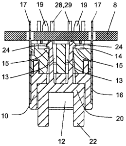
In order to realize a non-interchangeable mating of two connectors (1, 2), an encoding is provided on the mating side which is realized in the form of lami-nar encoding elements (20) that can be inserted into a slot (12) in the con-nector body (10) of the connectors. In this case, an encoding element (20, 20') that features mutually engaging structures (22, 22) for realizing an encodable mating is inserted into each of the connectors (1, 2).


French Abstract

Afin de réaliser l'appariement non interchangeable de deux connecteurs (1, 2), un codage est réalisé du côté appariement, sous la forme d'éléments de codage laminaires (20) insérables dans une fente (12) du corps des connecteurs (10). Dans ce cas, un élément de codage (20, 20') caractérisé par des structures à engagement mutuel (22, 22), qui permettent de réaliser un appariement codable, est inséré dans chacun des connecteurs (1, 2).

Claims

Note: Claims are shown in the official language in which they were submitted.


-8-

CLAIMS:


1. An encoding arrangement for a pair of mating electrical connectors for
achieving a non-interchangeable mating of the connectors, each connector
having a connector body with a mating side with electrical contacts,
comprising:
a slot provided in each of the connector bodies on the mating side, for
respectively receiving one of a pair of encoding elements of laminar design,
and
openings for electric contacts arranged to both each side of each slot, and
wherein the pair of encoding elements each have a tip on the mating side, the
tips
of the encoding elements being provided with complementary encoding structures

for non-interchangeable mating abutment of the encoding elements, the encoding

structures engaging into one another when the connector bodies are in mating
engagement, the encoding structures featuring vertical, horizontal, oblique
and
curve-shaped mating lines.


2. An encoding arrangement for a pair of mating electrical connectors for
achieving a non-interchangeable mating of the connectors, each connector
having a connector body with a mating side with electrical contacts,
comprising:
a slot provided in each of the connector bodies on the mating side, for
respectively receiving one of a pair of encoding elements of laminar design,
and
openings for electric contacts arranged to each side of each slot, and wherein

outer edges of the encoding elements are provided with complementary encoding
structures for non-interchangeable mating abutment of the encoding elements,
and the outer edges abutting one another in a precisely fitted fashion when
the
connector bodies are in mating engagement, the encoding structures featuring
vertical, horizontal, oblique and curve-shaped mating lines.


3. The encoding device according to claim 1 or 2, wherein each encoding
element features snap-in hooks for holding the encoding element in the slot of
the
connector body.


-9-

4. The encoding device according to claim 3 wherein the encoding structures
of the encoding elements respectively protrude from the slot on the mating
side of
the connector body.


5. The encoding device according to claim 1 or 2, wherein the electric
contacts are signaling contacts or current/voltage contacts.

Description

Note: Descriptions are shown in the official language in which they were submitted.


CA 02621722 2008-02-15
-1-

ENCODING DEVICE FOR CONNECTORS
BACKGROUND OF THE INVENTION

1. Field of the Invention

The invention pertains to an encoding device in a connector housing
with electric contacts in order to realize a non-interchangeable mating
of a two-part plug-type connection.

An encoding device of this type is required for preventing an incorrect
mating within a system of identical connectors.

2. Description of the related art

DE 298 23 719 U1 discloses an encoding device for two complemen-
tary connectors, one of which is provided with at least one first encod-
ing element and the other one of which is provided with at least one
complementary second encoding element, wherein at least one of the
connectors comprises a housing with a slip-on coupling ring, on which
at least one of the encoding elements is arranged.

The disadvantage of known encoding devices can be seen in that they
are retrospectively designed for the corresponding connector type and
therefore usually represent supplementary solutions.


CA 02621722 2008-02-15
-2-
SUMMARY OF THE INVENTION

The invention is based on the objective of ensuring the simple, non-
interchangeable and codable mating of a plug-type connection between
hybrid connectors to be mated which features power contacts as well
as signaling contacts.
This objective is attained in that a slot is provided in each of the con-
nector bodies on the mating side, wherein an encoding element of
laminar design is inserted into said slot, and in that additional openings
for electric contacts are arranged to both sides of the slot.
The advantages attained with the invention can be seen, in particular,
in that an essentially arbitrary number of encoding structures for mutu-
ally matible encoding elements inserted into the connector body of two
connectors to be mated can be realized with a relatively simple design
that features straight, vertical, horizontal, oblique and curved lines.

For this purpose, the connector body accommodating the electric con-
tacts is provided with a slot on the mating side, wherein the encoding
elements of laminar design are inserted and engaged in said slots. In
this case, the outer edges of the encoding elements preferably abut
one another in a precisely fitted fashion during the mating process.
Electric contacts arranged above and underneath the slot are sepa-
rated in accordance with signaling contacts and current/voltage con-
tacts.

The increased distance with the additional air gap contributes to an ad-
vantageous signal separation in this case.

The slots are only insignificantly larger than the disk-shaped encoding
elements and provided with passageways, through which snap-in hooks


CA 02621722 2008-02-15
-3-

are guided which are molded onto the encoding elements and can be
engaged on retaining edges on the cable connection side of the respec-
tive connector body.

In this case, engaged encoding elements can also be removed again
from the slots or exchanged.

The protection of the contacts and the encoding structures of the en-
coding elements, which protrude from the connector body, is realized in
the form of a correspondingly designed metallic shielding sleeve that
surrounds the connector body.

In this case, a V-shaped polarization moulded into the shielding sleeve
initially ensures a correct mating position of both connectors during the
mating process while the complementary encoding elements ensure
that exactly these two connectors can be correctly mated if a multitude
of possible plug-type connections can be realized.

BRIEF DESCRIPTION OF THE DRAWINGS

One embodiment of the invention is illustrated in the figures and descri-
bed in greater detail below. The figures show:

Fig. 1 is a connector in the form of a side view;

Fig. 2 is a connector realized in the form of a flanged housing;
Fig. 3 is a section through the connector in the flanged housing;

Fig. 4 is a section through a mated connection between the two con-
nectors shown in Fig. 1 and Fig. 2, and


CA 02621722 2008-02-15
-4-

Fig. 5 are several variations of encoding elements.
DESCRIPTION OF THE PREFERRED EMBODYMENTS

Figure 1 shows a side view of a connector 1 that is realized in accor-
dance with the so-called push-pull principle.

In this case, part of a shielding sleeve 16 that surrounds the electric
contacts 28, 29 is illustrated in a sectioned fashion such that the tip of
an inventive encoding element 20 is still visible. The signaling contact
29 is not visible in this figure.

The shielding sleeve 16 is arranged on a connector body 10 that ac-
commodates the electric contacts within a displaceable outer sleeve 2.
Figure 2 shows an isometric representation of a mating connector 5
that is realized complementary to the connector 1 and the connector
body 10 of which is arranged in a flanged housing 6.

Three adjacently positioned electric contacts 28 for a current/voltage
transmission, as well as four additional signaling contacts 29 that are
separated from one another by a larger average distance in a paired
fashion, are illustrated in the connector body 10. The contacts are ar-
ranged within the openings 28' and 29' in the connector body 10, 10'.
A slot 12 is provided between the differently designed electric contacts
on the mating side, wherein this slot is provided for accommodating a
laminar encoding element 20.


CA 02621722 2008-02-15
-5-

The rectangular insulating connector body 10 is surrounded by a shield-
ing sleeve 16, the seam of which extends in a V-shaped central groove
18 between the pairs of signaling contacts 29.

In this case, the groove is provided as a polarization for ensuring the
correct mating of the two connectors 1, 5.

On the rear side, the electric contacts are connected to a circuit board
8. The encoding element 20 may have different geometrical shapes on
its mating side. It would be possible to realize simple horizontal and
vertical outer edges, as well as oblique and curve-like shapes.

It is merely important that the outer edges provided for the encoding
abut one another in a precisely fitted fashion during the mating process
so as to prevent the incorrect mating of two connectors 1 and 5.

The sectional representation of the connector body 10 in Figure 3
through the plane of the encoding element shows the position and the
fixing of the encoding element 20 on the example of the connector 5
without the surrounding flanged housing 6.

The encoding element 20 is respectively inserted into the slot 12 on the
mating side and engaged in the connector body 10 by means of snap-in
hooks 24, wherein the encoding structures 22 partially protrude from
the connector body.

For this purpose, one respective passageway 13 for the two snap-in
hooks 24 in provided in the connector body 10 adjacent to the slot 12
for the encoding element 20.

On the connection side with the circuit board 8 and, in general, also on
an electric cable to be connected to the connector 1, the ends of the


CA 02621722 2008-02-15
-6-

passageways 13 respectively feature a retaining age 15, on which the
snap-in box 24 of the encoding element 20 engage.

In this case, the retaining edges 15 are molded into a sunk recess 14 in
the rear side of the connecting body in such a way that the snap-in
hooks only protrude minimally over the end of the housing.

As long as the connector is not yet soldered to the circuit board 8, the
encoding element 20 can be exchanged by pressing together the snap-
in hooks 24 and pulling the encoding element out of the passageways
13 and the slot 12.

The rear side of the connector 2 that is usually realized with the flanged
housing 6 is provided with a circuit board 8, to which the current/voltage
contacts 28, the signaling contacts 29 and the connecting pins 17 of the
shielding sleeve 16 are soldered.

In order to realize the mounting on the circuit board 8, the connector
body 10 is provided with additional mounting pin 19 that are inserted
into corresponding bores and hold the connector body together until it is
soldered to the circuit board.

Figure 4 shows the plug-type connection between the push-pull con-
nector 1 and the mating connector 5 in the flanged housing 6, wherein
this figure only shows the encoding of both encoding elements 20 and
20' in the connector 2 and the connector 1.

This figure also shows that the encoding structures 22, 22' protrude
from each of the connector bodies 10, 10' about centrally and into the
respective oppositely arranged part.


CA 02621722 2008-02-15
-7-

Figure 5 shows a few laminar embodiments of encoding elements 20,
20' that can be connected in a paired fashion and feature snap-in
hooks 24, 24', wherein said encoding elements may, in principle, have
any number of matching encoding structures 22, 22' with straight, verti-
cal, horizontal, oblique and curved lines.

Representative Drawing
A single figure which represents the drawing illustrating the invention.
Administrative Status

For a clearer understanding of the status of the application/patent presented on this page, the site Disclaimer , as well as the definitions for Patent , Administrative Status , Maintenance Fee  and Payment History  should be consulted.

Administrative Status

Title Date
Forecasted Issue Date 2012-06-12
(22) Filed 2008-02-15
Examination Requested 2008-02-15
(41) Open to Public Inspection 2008-08-15
(45) Issued 2012-06-12

Abandonment History

There is no abandonment history.

Maintenance Fee

Last Payment of $624.00 was received on 2024-02-06


 Upcoming maintenance fee amounts

Description Date Amount
Next Payment if standard fee 2025-02-17 $624.00
Next Payment if small entity fee 2025-02-17 $253.00

Note : If the full payment has not been received on or before the date indicated, a further fee may be required which may be one of the following

  • the reinstatement fee;
  • the late payment fee; or
  • additional fee to reverse deemed expiry.

Patent fees are adjusted on the 1st of January every year. The amounts above are the current amounts if received by December 31 of the current year.
Please refer to the CIPO Patent Fees web page to see all current fee amounts.

Payment History

Fee Type Anniversary Year Due Date Amount Paid Paid Date
Request for Examination $800.00 2008-02-15
Application Fee $400.00 2008-02-15
Section 8 Correction $200.00 2008-08-20
Maintenance Fee - Application - New Act 2 2010-02-15 $100.00 2010-01-08
Maintenance Fee - Application - New Act 3 2011-02-15 $100.00 2010-12-16
Maintenance Fee - Application - New Act 4 2012-02-15 $100.00 2011-12-13
Final Fee $300.00 2012-03-30
Maintenance Fee - Patent - New Act 5 2013-02-15 $200.00 2013-01-25
Maintenance Fee - Patent - New Act 6 2014-02-17 $200.00 2014-01-08
Maintenance Fee - Patent - New Act 7 2015-02-16 $200.00 2015-01-21
Maintenance Fee - Patent - New Act 8 2016-02-15 $200.00 2016-01-20
Maintenance Fee - Patent - New Act 9 2017-02-15 $200.00 2017-01-25
Maintenance Fee - Patent - New Act 10 2018-02-15 $250.00 2018-02-02
Maintenance Fee - Patent - New Act 11 2019-02-15 $250.00 2019-02-01
Maintenance Fee - Patent - New Act 12 2020-02-17 $250.00 2020-02-07
Maintenance Fee - Patent - New Act 13 2021-02-15 $255.00 2021-02-01
Maintenance Fee - Patent - New Act 14 2022-02-15 $254.49 2022-02-01
Maintenance Fee - Patent - New Act 15 2023-02-15 $473.65 2023-02-01
Maintenance Fee - Patent - New Act 16 2024-02-15 $624.00 2024-02-06
Owners on Record

Note: Records showing the ownership history in alphabetical order.

Current Owners on Record
HARTING ELECTRIC GMBH & CO. KG
Past Owners on Record
DE VANSSAY, JEAN-MERRI
MERMAZ, ALEXANDRE
Past Owners that do not appear in the "Owners on Record" listing will appear in other documentation within the application.
Documents

To view selected files, please enter reCAPTCHA code :


To view images, click a link in the Document Description column. To download the documents, select one or more checkboxes in the first column and then click the "Download Selected in PDF format (Zip Archive)" or the "Download Selected as Single PDF" button.

List of published and non-published patent-specific documents on the CPD .

If you have any difficulty accessing content, you can call the Client Service Centre at 1-866-997-1936 or send them an e-mail at CIPO Client Service Centre.


Document
Description 
Date
(yyyy-mm-dd) 
Number of pages   Size of Image (KB) 
Claims 2010-02-17 1 30
Cover Page 2008-08-08 1 40
Claims 2010-07-22 1 32
Abstract 2008-02-15 1 12
Description 2008-02-15 7 209
Claims 2008-02-15 1 34
Drawings 2008-02-15 5 57
Representative Drawing 2008-07-29 1 13
Cover Page 2010-06-07 2 69
Claims 2011-08-16 2 56
Claims 2011-03-28 2 55
Cover Page 2012-05-15 1 40
Prosecution-Amendment 2010-02-17 3 126
Prosecution-Amendment 2011-06-09 2 85
Correspondence 2008-10-06 1 12
Prosecution-Amendment 2010-07-22 4 173
Assignment 2008-02-15 4 104
Correspondence 2008-08-20 4 92
Prosecution-Amendment 2009-08-26 2 73
Correspondence 2010-02-17 3 81
Prosecution-Amendment 2011-08-16 4 150
Prosecution-Amendment 2010-05-28 2 60
Prosecution-Amendment 2010-06-07 2 48
Prosecution-Amendment 2010-12-09 2 71
Prosecution-Amendment 2011-03-28 4 178
Correspondence 2012-03-30 1 29