Note: Descriptions are shown in the official language in which they were submitted.
CA 02621924 2008-03-05
Express Mail Label No. EV696282616US
Date of Deposit: 05 September 2006
Atty. Docket No. 0112020.00211 WOI (NAN-75)
Carbon Nanotubes for the Selective Transfer of Ileat froni Electronics
Cross-Reference to Related Applications
[0001] This application claims the benefit under 35 U.S.C. 119(e) of U.S.
Provisional Patent Application No. 60/714,386, filed September 6, 2005 and
entitled
"Carbon Nanotubes for the Selective Transfer of Heat from Electronics," the
entire
contents of which are incorporated herein by reference.
Background
Technical Field
(0002] The present application relates generally to nanotube fabrics and
methods of
malcing saine.
Discussion of Related Art
[0003] As ultra-large-scale-integration of integrated circuits,
microelectronic
components and devices are becoming increasingly more dense and compact, there
exists
an increasing need for smaller and more potent heat transfer devices due to
the excessive
on-chip heat generatioii. Current integrated circuits used in microprocessors
operated at
liigh freduencies use power densities on the order of 50 W/cmZ: in
coinparison, a 60 W
light bulb generates 0.5 W/cm2. Such power densities lead to highly localized
heating of
integrated circuits in areas known as "liot spots".
(0004] As the rise in power density increases, the number of hot spots" on
the
surface of high power chips increases as observed in microprocessors. Cooling
microprocessors is generally necessary to prevent device degradation and to
achieve the
best possible device performance. A maximum safe temperature for integrated
circuit
(IC) operation is typically between 100-120 C.
l
CA 02621924 2008-03-05
Express Mail Label No. EV696282616US
Date of Deposit: 05 September 2006
Atty. Docket No. 0112020.0021 1 WQ1 (NAN-75)
100051 Solving the problems that "hot spots" present is imperative for the
next-
generation IC packages, as there is an ever-increasing need for smaller-scale
devices.
Carbon nanotubes (CNTs) are being used in many different applications in the
field of
electronics and are found to be extremely useful due to their electrical,
mechanical,
optical, chemical and thermal properties.
100061 Carbon nanotubes, with tube diameters around 1-2 nm, are electricai
conductors that are able to carry extremely high current densities. They also
have the
highest known thermal conductivity, and are also generally thermally and
chemically
stable. Further details on characteristics of carbon nanotubes may be found in
the
following references, the entire contents of which are incorporated herein by
reference: Z.
Yao, C.L. Kane, C. Dekker, Phys_ Rev. Lett. 84, 2941 (2000); P.M. Ajayan, T.W.
Ebbesen, Rep. Prog. Phys. 60, 1025 (1997); Savas Berber, Young-Kyun Kwon and
David
Tomanek, "Unusually High Thennal Conductivity of Carbon Nanotubes," Phys. Rev.
Lett. 84(20), 4613-4616 (2000); Jianwei Che, Tahir Cagin and William A Goddard
III,
"Thermal conductivity of carbon nanotubes," Nanotechnology, 11, 65-69, 2000;
J. Hone,
M. Whitney and A Zettl, "Thermal conductivity of single-walled carbon
nanotubes,"
Synthetic Metals, 103-2498-2499, 1999 and Mohamed A Osman and Deepak
Srivastava,
"Temperature dependence of the thermal conductivity of single-wall carbon
nanotubes,"
Nanotechnology, 12, 21-24, 2001.
(0007) Using individual nanotubes for heat transfer, however, can be
problematic
because of difficulties in growing them with suitably controlled orientation,
lengtli, and
the like.
10008) There is a need in the art for very effcient, very small, even
submicron-sized,
heat transfer elements which are easily fabricated and are compatible with
electronics
applications and fabrication techniques. There is likewise a need in the art
for large scale
fabrication methods of heat transfer devices used for electronic applications
in the
semiconductor industry which can be monolithically integrated into a CMOS or
similar
2
CA 02621924 2008-03-05
Express Mail Label No. EV696282616US
Date of Deposit: 05 September 2006
Atty. Docket No. 01 12020.0021 I W OI (NAN-75)
process flow to fabricate integated circuits. Naturally, the uses of such
elements extend
to most types of consumer electronics where heat transfer in integrated
elements is
beneficial.
Summary
100091 The present invention provides carbon nanotubes for the selective
transfer of
heat from electronics.
[0010] Under one aspect, a method of cooling a circuit element includes
providing a
thermal reservoir liaving a temperature lower than an operating temperature of
the circuit
element; and providing a nanotube article in thennal contact with the circuit
element and
with the reservoir, the nanotube article including a non-woven fabric of
nanotubes in
contact with other nanotubes to define a plurality of thermal pathways along
the article,
the nanotube article having a nanotube density and a shape selected such that
the
nanotube article is capable of transferring heat from the circuit element to
the thennal
reservoir.
[0011] One or more embodiments include one or more of the following features.
Providing the nanotube article includes depositing pre-formed nanotubes on a
surface so
as to form the non-woven fabric of nanotubes. Depositing pre-foirned nanotubes
includes
at least one of spin-coating pre-formed nanotubes and spray-coating pre-formed
nanotubes. Providing the nanotube article includes growing nanotubes on a
surface so as
to form the non-woven fabric of nanotubes.
(0012) Further including defining the shape of the nanotube article
lithographically.
Defining the shape of the nanotube article lithographically includes forn-ting
a non-woven
fabric of nanotubes and subsequently removing selected portions of that non-
woven
fabric of rianotubes in accordance with the shape. Providing the nanotube
article includes
conformally fonning a non-woven nanotube fabric over the circuit element. The
nanotube article has a substantially planar shape. Further including providing
a substrate
3
CA 02621924 2008-03-05
Express Mail Label No. EV696282616US
Date of Deposit: 05 September 2006
Atty. Docket No. 0112020.00211 WO 1(NAN-75)
having a substantially planar major surface and a feature not in the plane of
the major
surface, and wherein the nanotube article substantially conforms to said
feature. Further
including providing supports under the nanotube article, the supports defining
a gap over
which the nanotube article is suspended. The nanotube density and shape are
selected
such that the nanotube article is capable of transferring lieat from the
circuit element to
the thermal reservoir at a pre-defined rate selected to maintain the circuit
element below a
pre-specified temperature. The pre-specified temperature includes an upper
limit of a
nornial operating temperature. The nanotube article further has a pre-defined
composition. The pre-defined composition includes single-walled nanotubes. The
pre-
defined composition includes multi-walled nanotubes. The circuit element
includes at
least a portion of an integrated circuit. The circuit element includes an
encapsulation
material. The thennal reservoir includes a heat sink. The heat sink includes a
plurality of
fins that radiate heat. Further including a thermally conductive material
between and in
thermal contact with each of the nanotube article and the circuit element.
10013] Under another aspect, a naethod of forming a thennal management
structure
for an integrated circuit includes depositing a layer of pre-formed nanotubes
on a defined
region of the integrated circuit, the layer substantially confonning to the
defined region of
the integrated circuit and including a plurality of nanotubes; and providing a
thermal
reservoir in thermal contact with at least a portion of the layer of
nanotubes, wherein the
layer of pre-formed nanotubes has a nanotube density selected such that the
nanotube
article is capable of transferring heat from the integrated circuit to the
thermal reservoir_
(0014) One or more embodiments includes one or more of the following features.
Depositing the layer of pre-fonned nanotubes includes at least one of spin-
coating and
spray-coating pre-fonned nanotubes onto the defined region of the integrated
circuit.
Further including patterning the layer of pre-formed nanotubes to provide
defined regions
of nanotubes over pre-selected portions of the integrated circuit. T1ie
defined regions of
nanotubes are each in tliermal contact with the tliermal reservoir. The pre-
selected
portions of the integrated circuit include portions of the circuit needing
cooling during
4
CA 02621924 2008-03-05
Express Mail Label No. EV696282616US
Date of Deposit: 05 September 2006
Atty. Docket No. 0112020.0021 l WO1 (NAN-75)
operation. The pre-selected portions of the integrated circuit include
individual devices
within the integrated circuit. The pre-selected portions of the integrated
circuit include
active regions of the integrated circuit. The layer of pre-formed nanotubes
includes
providing a patterned mask over the layer of pre-formed nanotubes and removing
a
portion of the layer of pre-formed nanotubes in accordance with the patterned
mask.
Patterning the layer of pre-formed nanotubes further includes defining at
least one of a
memory element, a heat emitter, a channel in a field effect transistor, a gate
in a field
effect'transistor, a relay, a conductor, and a sensor within the layer of pre-
formed
nanotubes. Further including patterning the layer of pre-formed nanotubes to
define
regions of modified thermal conductivity. Further including functionalizing at
least a
portion of the nanotubes of the layer of pre-formed nanotubes. The integrated
circuit is
substantially encapsulated. The integrated circuit is substantially complete
before
depositing the nanotube layer thereon. Further including providing a second
integrated
circuit over the previously mentioned integrated circuit with the layer of pre-
formed
nanotubes there between, the layer of pre-formed nanotubes being in thermal
contact with
the second integrated circuit. The nanotubes of the layer of pre-formed
nanotubes
includes define a plurality of thermal pathways within the layer of pre-fonned
nanotubes.
The layer of pre-formed nanotubes includes a non-woven fabric of entangled
nanotubes.
At least some of the nanotubes of the layer of pre-formed nanotubes I-iave a
length of at
least 100 nm. The layer of pre-formed nanotubes has a thickness between about
I nm and
about 100 nm. The layer of pre-formed nanotubes is substantially a monolayer
of
nanotubes. The defined region of the integrated circuit includes the top
surface of the
integrated circuit.
Brief Description of the Drawings
[00151 In the Drawing:
Figure 1 illustrates an embodiment of a lateral heat transfer structure;
CA 02621924 2008-03-05
Express Mail Label No. EV696282616US
Date of Deposit: 05 September 2006
Atty. Docket No. 01 12020.00211 W0] (NAN-75)
Figures 2A and B are micrographs of nanotube fabrics and pattcrning thereof;
Figure 3 illustrates an embodiment of a vertical heat transfer structure;
Figures 4A-4C are micrographs of conformal nanotube fabrics;
Figure 5 illustrates an embodiment of a partially suspended heat transfer
structure;
Figure 6 illustrates an embodiment of an array heat transfer structure;
Figure 7 illustrates a conventional heat sink on an integrated circuit;
Figures 8A and 8B illustrate embodiments of heat transfer structures used to
transfer heat from an integrated circuit; and
Figure 9 illustrates an embodiment of a heat transfer structure used to
transfer heat
from a stack of wafers.
Detailed Description
10016J Non-woven fabrics of carbon nanotubes (CNTs) can help manage the
problein of thermal "hot spots" and heat transfer in high power devices. CNT
fabrics
have superior thennal conductance relative to single nanotube as well as to
conventional
conductive materials such as metals, and therefore the CNT fabrics have a
tremcndous
potential for providing extremely efficient heat transfer. CNTs exhibit a very
lligh "axial"
thermal conductivity. For a discrete multiwalled nanotube (MWNT), the thermal
conductivity is expected to surpass 3000 W/m-k along the tube axis, while
theoretical
studies of single walled nanotubes (SWNTs) have shown that thermal
conductivities of
6600 W/m-K are possible. CNT fabrics can be used as effective heat-sinks,
which are
able to remove large ainounts of heat away from critical "hot spots".
[0017) Preferred embodiments of this invention use CNT fabrics for the
transfer of
heat away from heat sensitive areas in an electronic circuit or from an entire
electronic
6
CA 02621924 2008-03-05
Express Mail Label No. EV696282616US
Date of Deposit: 05 September 2006
Atty. Docket No. 0112020.00211 W01 (NAN-75)
chip. Similar to other carbon allotropes, CNTs have a high thermal
conductivity, where
thermal conductivity is defined as the ability of a material to remove heat by
a
relationship between the negative teniperature gradient and the ratio of the
heat flow rate
per unit area. Thermal conductivity is defined by the equation ~Q ~=-K ~X ,
where tc is
the thermal conductivity of the material, Q is the quantity of heat in Joules,
t is time in
seconds, A is area-m2, temperature (T) is measured in degrees K, and x is
measured in
meters. The thermal conductivity of a material is dictated by electronic
and/or phonon
propagation and the thermal conductivity of materials will add in parallel;
therefore, for
multiple metal lines in parallel, the heat transfer rate can be calculated by
using equation:
dQ k'A' +kzAZ+...+k"A" xVz-'l,)
dt d, d2 dõ )
(0018] Unlike the other forms of carbon, the thermal conductivity of nanotubes
is
confined along the axis of the nanotube due to its l-D structure. The thermal
conductivity
of CNTs is theoretically predicted to be greater than about 2000 W/m-K, with
values of
6600 W/m-K possible, while experimental measurements have demonstrated thermal
conductivity of greater than about 200 W/m-K at room temperature comparable to
bulk
Cu (about 400 W/m-K) and bulk A] (about 300 W/m-K) at room temperature. The
disparity between theoretical and experimental results is typically attributed
to
deformations along the structure of the CNTs and the effects of non-ideal
contacts and
test set-up for the measuring of thermal conductivity. Unlike high thermal
conductivity
metals, CNTs are easily deposited and patterned to nanometer dimensions, the
thermal
conductivity of the nanotubes do not decrease with increased temperature
(typically up to
about 500 K) and CNTs have a high melting point (typically over about 3000 K).
SWNTs
also typically possess the ability to carry a high current density (e.g., over
about I09
A/cmz) and the nanotubes do not readily react/diffuse with their sun-oundings,
unlike
conventional higl>ly thermally conductive materials such as metals. The
combination of
these unique properties makes CNT fabrics useful for the thermal management of
heat
7
CA 02621924 2008-03-05
Express Mail Label No_ EV696282616US
Date of Deposit: 05 September 2006
Atty. Docket No. 0112020.0021 1 WO1 (NAN-75)
sensitive areas on a semiconductor chip, 3-D stacked wafers and other
applications where
removal of heat is required.
100191 CNT fabrics have several features that can be useful for heat transfer
and are
not generally available with conventional heat transfer technologies. First,
the very layer
of fabric used to make the heat transfer element can also be used to make
other electronic
elements on the same substrate. For example, a single CNT fabric can be
pattemed to
produce different regions that may be utilized, e.g., as heat transfer media,
memory
elements, heat emitters, channels or gates in field effect transistors,
relays, conductors,
electrical insulators, and/or sensors, or a plethora of other types of
elements depending on
how the sections of the fabric are patterned and processed. Examples of
nanotube fabric
devices and methods of making same may be found in the incorporated patent
references,
given below. Second, VLSI arrays of these CNT heat transfer fabrics can be
formed
using patterning technology at minimum dimensions of the lithography node
used, e.g.,
giga-sized CNT heat emitter arrays can be fabricated at 180 nm or smaller
critical feature
size. Such methods are more fully described in the incorporated patent
references. Third,
such nanofabric-based heat transfer fabrics devices scale directly with the
lithographic
ground rule used, such that, e.g., 180 nm, 130 nm, 90 nm and 65 nm sized
emitters can be
produced.
100201 Under certain embodiments of the invention, the heat transfer articles
may be
made from a nanotube non-woven fabric, layer or film, typically of entangled
or matted
nanotubes, which in some cases may be pattemed into ribbons or belts. Creating
ribbons
or belts (more generally referred to as "traces") of pattemed nanotube fabrics
overcomes
many of the difficulties that inay arise in attempting to grow "aligned" CNTs
with
controlled orientation, length, and the like. Creating traces from nanotube
fabrics allows
the traces to retain many if not all of the benefits of individual nanotubes.
Moreover,
traces made from nanotube fabric have benefits not found in individual
nanotubes. For
example, since the traces include many nanotubes in aggregation, the traces
will generally
not fail as the result of a failure or break of an individual nanotube.
Instead, there are
8
CA 02621924 2008-03-05
Express Mail Label No. EV696282616US
Date of Deposit: 05 September 2006
Atty. Docket No. 0112020.0021 I W O 1(NAN-75)
many alternate paths tlu-ough which heat (e.g., phonons) may travel within a
given trace.
In effect, a trace made from nanotube fabric defines a heat transfer network
of individual
nanotubes, each of which conducts heat. Moreover, by using nanotube fabrics,
layers or
films, current technology may be used to create such traces.
[0021) The nanotube fabric may be disposed on the substrate and may be created
by
spin coating, spray coating, direct growth, or any other appropriate method.
After the
CNT fabric is deposited, the fabric can be pattemed to make heat transfer
ribbons, e.g.,
using standard CMOS lithographic and etching processes. For example, Fig. 2
shows a
CNT fabric that has been pattemed to have nanometer sized dimensioiis, here a
250 nm
ivide CNT pattern (more on this below). Unlike more conventional techniques
which
typically rely on directed growth or chemical self-assembly of individual
nanotubes,
preferred embodiments utilize fabrication techniques involving thin films and
in most
cases, lithography, which allow fabrication over large surface-i.e. >6"
silicon based
substrates used for electronic circuits. (In contrast, growing individual
nanotubes over a
distance beyond sub niillimeter distances is typically unfeasible.) Exemplary
methods of
malcing and patterning nanotube fabrics may be found in the incorporated
patent
references.
[0022] Once the CNT fabric has been pattemed, further processing can then be
performed, typically without damaging the properties and characteristics of
the pattemed
CNT fabric. For example, the CNT fabric can be exposed to various metal
deposition
methods, various etching methods and various corrosive and reductive
atmospheres,
generally without any degradation of the CNT fabnc's properties.
[0023J CNT fabrics are generally easily manufactured and fabricated using
standard
front-end and back-end CMOS integration equipment and techniques. Highly
conductive
metals such as copper, on the other hand, require electro-deposition and
Chemical-
Mechanical-Planarization (CMP) techniques to create damascene structures to
use on the
chip; such techniques require large areas of chips. CNTs do not typically
require large
9
CA 02621924 2008-03-05
Express Mail Label No. EV696282616US
Date of Deposit: 05 September 2006
Atty. Docket No. 0112020.00211 WO1 (NAN-75)
amounts of surface space and may be easily patterned, e.g., with oxygen
plasmas. The
thermal conductivity of copper generally decreases with shrinking feature
size. In
contrast, as the size of CNT fabric-based heat transfer devices decrease, the
number of
conductive tubes decreases, so the overall thermal conductance (generally the
thermal
conductivity times cross-sectional area divided by length) decreases, however
the
individual CNT thermal conductivity remains the same.
[0024) The themnal conductivity of a monolayer fabric is generally greater
than that
of a single carbon nanotube due to the additive effects of the multiple heat
conducting
tubes. The thermal conductivity of a monolayer fabric is also generally
greater than a
layer of copper with the same geometry, due to the greater thermal
conductivity per cross
sectional area of carbon nanotubes as compared to copper. CNTs also do not
typically
interact with surrounding materials, as copper does. For example, CNTs will
not
generally diffuse through various material layers and alter/destroy active
regions of
electronic devices (i.e. the active conductive channel of Si MOS devices),
therefore, there
is no need to take precautions against this when using CNTs as would be
necessary when
using copper (which is a deep level trap for silicon).
100251 The ability to deposit and pattem the CNT fabric allows for the
creation of
CNT heat pipes/channels on-chip that can transfer large amounts of thermal
power away
from sensitive active regions on semiconductor electronics. Figure 3
illustrates a cross
section of an exemplary device.
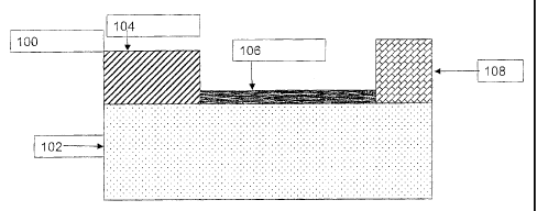
(0026) An embodiment of a simple heat transfer structure 100 is illustrated in
figure
1. Structure 100 includes a substrate 102, a heat load 104, a heat transfer
fabric 106 and a
heat reservoir 108. Fabric 106 is in thermal contact with heat load 104 and
with heat
reservoir 108, and transfers heat from heat load 104 to heat reservoir 108.
This structure
is shown only as an example, any architecture may be used in which the
geometry is
arranged so that the nanotube fabric can transfer heat from a(hatter) thermal
load to a
(cooler) thermal reservoir, and the nanotube fabric has a size, shape, and
nanotube density
CA 02621924 2008-03-05
Express Mail Label No. EV696282616US
Date of Deposit: 05 September 2006
Atty. Docket No. 0112020.00211 W O 1(NAN-75)
(e.g., thickness) selected to transfer a sufficient amount of heat from the
thermal load to
the thermal reservoir. For example, a fabric used to cool a conventional
integrated circuit
would generally have a size and shape sufficient to cover the parts of the
integrated
circuit that need cooling, and the fabric would have enough nanotubes (of the
correct
type) to transfer heat from the integrated circuit to a thermal reservoir at a
rate sufficient
that the integrated circuit would remain at a safe operating temperature,
e.g., 100-120 C.
100271 In some embodiments a nanotube fabric is fabricated over an entire
wafer
surface, and then portions of the fabric are removed by patterning, thereby
leaving heat-
transferring portions only in desired locations. Such patterning may be
accomplished by
using methods such as those in the incorporated patent references. Figure 2A
illustrates
patterned photoresist 202 disposed on a section of nanotube fabric 204
overlying a
substrate 206. According to one method of nanotube patteming, the exposed
fabric 204
and the resist 202 are exposed to an ashing procedure thereby removing the
exposed
nanotube fabric. The resist 202 is subsequently removed, and the patterned
fabric 208
remains, as shown in figure 2B. Figure 2B illustrates a patterned, relatively
sparse
nanotube fabric 208. In a configuration such as that shown in Fig. I, such a
fabric is
capable of conducting heat away from a "hot spot" such as heat load 104, to a
thermaI
reservoir (in some cases referred to as a"heat sink," such as thermal
reservoir 106.
[0028) A second exemplary device 300 that could be used for on-chip thermal
management of high heat load active regions is illustrated in figure 3. Device
300 has a
higli heat load active region 302, a low-thermal conductivity region 304 (such
as silicon
or silicon dioxide), a moderate to high thermal conductivity region 306 (such
as an
interconiiect metallization layer), a nanotube fabric 308 and a thermal
reservoir region
310. Fabric 308 is in thennal contact with lleat load active region 302 via
moderate to
high thermal conductivity region 306, and with thertnal reservoir region 310.
In
operation, heat flows from heat load 302, through moderate to higli thermal
conductivity
region 306, through nanotube fabric 308, and into reservoir 310. The geometry
and exact
relative placement of the elements of structure 300 need not be as described;
orte skilled
ll
CA 02621924 2008-03-05
Express Mail Label No. EV696282616US
Date of Deposit: 05 September 2006
Atty. Docket No. 0112020.00211 WO1 (NAN-75)
in the art will understand that as long as the geometry and composition of
fabric 308 is
configured to lead heat away from the lieat load active region 302 then the
thermal
transfer properties of the fabric 308 may be utilized.
100291 Nanotube fabrics and ribbons thereof have also been shown to
substantially
conform to a surface, such as a surface of an article on a semiconductor
substrate. For
example, the fabric is generally horizontally oriented when the surface of the
substrate
that receives the fabric is horizontally oriented, and the fabric is generally
vertically
oriented on a vertical surface of a suitable substrate. Fabrication techniques
to develop
such horizontally- and vertically-disposed fabrics and devices using such
nanottibe
fabrics, inay be created via CVD or by room temperature operations; further
details may
be found in the incorporated patent references. This feature allows nanotube
fabrics to
be used as heat transfer media on a wide variety of semiconductor substrates
and features.
Figures 4A-4C illustrate typical conformal properties of carbon nanotube
fabrics. Figure
4A is a micrograph of a patterned nanotube fabric 400 disposed upon a
substrate 402 with
raised features 404. Figures 4B and 4C are detailed micrographs of a nanotube
fabric 400
conforming to a substantially vertical substrate feature 404.
[0030] CNT fabrics can also be suspended by supports above the surface of the
substrate. Suspending heat transfer fabrics can enhance the ability of the
fabrics to
conduct heat while not being significantly influenced by the
surrounding/underlying
substrate since the suspension of the fabric will prevent any interaction
between the
substrate and the CNTs that may perturb the transfer of heat along the axis of
the CNTs
due to defon-nation caused in the tube because of the van der Waals forces
present on the
surface. Suspending the CNT fabric may also reduce or eliminate the
possibility of the
large surface area of the substrate retaining heat, which may prevent the CNT
fabric from
adequately transfetring the heat away from the active device.
100311 Figure 5 illustrates an exemplary structure 500 utilizing heat transfer
fabric
portions that are suspended over air/vacuum gaps. Structure 500 includes a
substrate 502,
12
CA 02621924 2008-03-05
Express Mail Label No. EV696282616US
Date of Deposit: 05 September 2006
Atty. Docket No_ 0112020_00211WO1 (NAN-75)
an active region 504, a low thermal conductivity layer 506, a moderate to high
thermal
conductivity region 508, air gaps 510, a suspended nanotube fabric 512 and a
thermal
reservoir 516. Gaps 510 are defined by supports in low thermal conductivity
layer 506,
beneath the nanotube fabric 512. Fabric 512 is in thermal contact with active
region 504
via moderate to high thermal conductivity region 508, and with thennal
reservoir region
516. In operation, heat flows from active region 504, through moderate to high
thermal
conductivity region 508, through nanotube fabric 512, and into reservoir 516_
[0032] As mentioned above, CNT fabrics can be applied to an entire wafer,
patterned,
and selected sections can be removed. Thus, heat-transfer sections can be left
in desired
locations to remove heat from selected sites. Therefore, any location on the
chip that is
highly sensitive to heat loads can have a patterned CNT heat transfer fabric
applied
adjacent to it in order to remove the excess heat load. Because the entire
wafer surface
may be covered with CNT fabric and selected portions of fabric can be removed
(or even
used as other electronic elements as described above), large arrays of CNT
heat pipes can
be fabricated in parallel. The lithography technology node used generally
dictates
minimum array spacing and size array size.
100331 Figure 6 is a plan view of an exemplary heat transfer fabric that has
been
pattemed to remove heat from many selected heat sensitive sites on a wafer
substrate.
Structure 600 has a substrate 602, heat sensitive active regions 604,
patterned CNT heat
transfer fabric regions 606, non-heat sensitive active regions 608 and a
thermal reservoir
610. Heat transfer fabric regions 606 are each in thermal contact with a
corresponding
heat sensitive active region 604, and with thermal reservoir 610. In
operation, heat flows
from active regions 604, through patterned CNT heat transfer fabric regions
606, and into
reservoir 610.
(0034] The substrate 602 is created and heat sensitive active regions 604, non-
heat
sensitive active regions 608 and a therrrmal reservoir 610 may be deposited on
or created
on the substrate 602. A carbon nanotube based fabric is then created, e.g. by
spin coating
13
CA 02621924 2008-03-05
Express Mail Labe] No. EV696282616US
Date of Deposit: 05 September 2006
Atty. Docket No. 0112020.0021 I WO1 (NAN-75)
or by aerosol application or dipping. The fabric is then patterned, and
selected regions of
the fabric are removed to create patterned CNT heat transfer fabric regions
606.
Nanotube fabric fabrication, patterning, and removal techniques may be found
in the
incorporated patent references.
100351 CNT fabrics can also be employed to transfer heat from entire chips to
external heat reservoirs. Figure 7 illustrates a prior art structure used for
the removal of
heat from an encapsulated cliip. Structure 700 includes an encapsulation
material 702,
terminals 704, contacts 706, a semiconductor chip 708, and a heat sink 710.
Typically,
"thermal grease" or another thermally conductive material is used to conduct
heat
between the encapsulated semiconductor chip 708 and the heat sirilc 710.
[00361 According to certain embodiments, nanotube fabrics, e.g., multilayered
(e.g.,
10-500 nm) nanotube fabrics can be used to transfer the heat from heat
sensitive
encapsulated areas on an electronic chip. Multilayered nanotube fabrics can be
formed,
e.g., by employing a spray coating process, or with other methods such as
those described
in the incorporated patent references. Two exemplary architectures for using a
nanotube
fabric to transfer heat fi-oin an encapsulated chip, e.g., an IC, are
illustrated in figures 8A
and 8B.
(0037) Figure 8A illustrates a structure 800 which includes encapsulation
matenal
802, terminals 804, contacts 806, a semiconductor chip 808, a heat sink 810,
and a heat-
conducting layer of nanotubes 812. The heat-conducting layer of nanotubes 812
is
disposed between the semiconductor chip 808 and the heat sink 810 so that it
can carry
heat from the chip to the heat sink.
100381 Figure 8B illustrates another exemplary heat transfer structure 850.
Structure
850 has encapsulation material 802, terminals 804, contacts 806, a
semiconductor chip
808, a thermal reservoir 852, (a metal cover may be used as a thermal
reservoir, for
example), and a heat-conducting layer of nanotubes 854; the layer of nanotube
fabric may
14
CA 02621924 2008-03-05
Express Mail Label No. EV696282616US
Date of Deposit: 05 September 2006
Atty. Docket No. 0112020.00211wO1 (NAN-75)
include a supporting layer. (The supporting layer is used to support the CNT
fabric until
it reaches the thermal sink. The substrate (not shown in the schematic) is
typically not
important to the design and operation of the chip.) Note that the nanotube
fabric layer in
the embodiment shown in Figure 8B has a non-planar configuration.
f 0039] Nanotube fabrics can also be used to remove licat from 3-D stacked
wafers.
Figure 9 illustrates a structure 900 that includes stacked chips (wafers) 902,
heat transfer
fabcic layers 904 and a thennal reservoir 906. As can be seen in figure 9, the
fabric layers
904 are disposed between, and preferably in thermal contact with, overlying
and
underlying (where applicable) stacked chips 902. The stacked chips 902 are
shown in
contact with a thennal reservoir 906, however the chips 902 need not be in
such contact.
The fabric heat transfer layers 904 are in thennal contact with the thermal
reservoir 906,
and conduct heat from the stack of wafers into the tliermal reservoir 906.
100401 When the heat transfer fabric is used with 3-D stacked wafers, the CNT
fabric
may be deposited in-between the wafers for example by spin-coating or spray-
coating.
The CNT fabric will then transfer any excess heat away from the mid-regions of
the stack
to an external thermal reservoir. The use of CNTs is advantageous over other
thennal
management technologies such as Cu in that the CNTs typically do not react
with the
surrounding substrates and therefore will not contaminate the sensitive
electronics, are
easily deposited, and have adjustable thickness that can be quite thin, e.g.,
a few
nanometers.
Other Embodiments
100411 The heat conduction properties of the nanotube fabrics may be altered
by
tailoring the composition, size, shape, andlor geometry of the CNT fabric. For
example,
thicker and denser fabrics will generally conduct more total heat than sparser
fabrics, and
wider fabrics will generally conduct more heat than narrower fabrics of the
same density.
Three-dimensional parameters of the fabrics may affect their thermal transport
properties
CA 02621924 2008-03-05
Express Mail Label No. EV696282676US
Date of Deposit: 05 September 2006
Atty. Docket No. 0112020.00211 WOI (NAN-75)
as well. The materials that contact the nanotube fabrics will also have an
effect on heat
transfer and/or dissipation. The heat conduction properties are also
controllable and
therefore tailorable by altering the coniposition of the nanotubes (i.e. SWNTs
and
MWNTs), etc_ The heat conduction properties of individual CNTs can be altered
by
functionalization, e.g., to restrict or enhance the transport of heat from the
thermal load.
Investigators have shown that functionalization of single-walled carbon
nanotubes
drastically reduces their thermal conductivities, see Padgett et al.,
"Influence of
Chemisorption on the Thermal Conductivity of Single-Wall Carbon Nanotubes,"
Nano
Letters, 4 (6), 1051-1053, 2004, the entire contents of which are incorporated
herein by
reference. This can be a useful feature in cases where there are some areas on
a given
wafer that do not require rapid transport of heat away from an active region.
[0042] There are several possible commercial applications for this product.
One such
application would be to regulate the amount of heat that is stored at
selective regions on
the chip. A second application involves the removal of large amounts of
therrnal power
from encapsulated chips and a third possible product would involve the removal
of heat
from 3-D stacked wafers.
(0043] Thougli rnost of the disclosure above is written as if the fabric were
made of
nanotubes of the same type, e.g., all single-walled, the fabrics may be
composed of all
multi-walled nanotubes or of a combination of single- and multi-walled
nanotubes.
[0044) The above-described embodiments of nanotube-based lieat transfer
elements
use traces of electrically conductive articles made from naiiotube layers 106,
such as
those shown in figures 1 and 2. The layers may have a minimum thickness of
about 10
nm or less, i.e., the thickness of a given nanotube, and a typical thickness
of about 50 nm.
Thicknesses greater than 50 nm are useful and the thickness is detennined
based on the
end use of the given transfer fabric. The fabrics may be patterned to a
minimum
dimension of 150 nni with a maximum width of several microns. 11ie wider
fabrics will
give a higher heat transfer rate due to the expected higher tliermal
conductivity of the
16
CA 02621924 2008-03-05
Express Mail Label No. EV696282616US
Date of Deposit: 05 September 2006
Atty. Docket No. 0112020.00211 WOI (NAN-75)
redundant tubes. Another important parameter includes the number of nanotubes
in the
fabric. Higher nanotube densities will give a higher overall thermal
conductivity of the
system due to the combined effect of the individual nanotubes. The thennal
transfer
length is also important. Minimum lengths of several hundred nanometers may
provide
superior heat transfer properties, while the thermal conductivity of the
system may be
expected to decrease with lengths up to several microns, due to serial
connection of
nanotubes, causing perturbations in the transport of heat. Heat transfer may
depend on
the thickness of the nanotube fabric as well, with thicknesses in the range of
10-100 nm
being envisioned for various applications. The nanotube matte is grown or
deposited on a
surface, such as that of a silicon wafer, to form a contiguous film of a given
density. The
same two dimensional film that may be patterned into discrete heat transfer
elements can
also be patterned to generate conductively interconnecting traces ranging in
width from I
nm (the intrinsic minimum size of a nanotube) to hundreds of microns or
greater,
depending on the application and context, as well as other electronic elements
as
described in incorporated references, including, but not limited to:
transistors, triodes and
memory elements.
Heat Transfer Ele ients with Dielectric Patterning
[0045] Heat transfer elements may be formed from a single layer of conducting
nanotube fabric where certain portions of the fabric are caused to become
insulating while
leaving other portions conductive. Further details on patteming dielectric
features into
nanotube fabrics may be found in U.S. Patent Applieation No. 11/398,126.
[0046] The following commonly-owned patent references, referred to herein as
"incorporated patent references," describe various techniques for creating
nanotube
elements (nanotube fabric articles and switches), e.g., creating and
patterning nanotube
fabrics, and are incorporated herein by reference in their entireties:
17
CA 02621924 2008-03-05
Express Mail Label No. EV696282616US
Date of Deposit: 05 September 2006
Attv. Docket No. 0112020.0021 I WO1 (NAN-75)
[0047) U.S. Patent Application No. 09/915,093, Electromechanical Meniory Array
Using Nanotube Ribbons and Method for Malang Sante, filed July 25, 2001, now
U.S.
Pat. NO. 6,919,592;
[00481 U.S. Patent Application No. 09/915,173, Electroniechanical Memory
Having
Cell Selection Circuilry Constructed tivith Nanotube 7eclznology, filed July
25, 2001, now
U.S. Patent No. 6,643,165;
(00491 U.S. Patent Application No. 09/915,095, Hybrid Circuit Having Nanotube
Electromechanical Memory, filed July 25, 2001, now U.S. Patent No. 6,574,130;
100501 U.S. Patent Application No. 10/033,323, Electr-omechanical Three-Ti=ace
Junction Devices, filed December 28, 2001 now U.S. Pat. No. 6,911,682;
[00511 U.S. Patent Application No. 10/802,900, Electromechanical Three-Ti-ace
Jiuzction Devices, filed March 17, 2004;
(00521 U.S. Patent Application No. 10/033,032, Methods ofMaking
Electromechanical Three-Trace.lurtction Devices, filed December 28, 2001, now
U.S.
Patent No. 6,784,028;
10053] U.S. Patent Application No. 10/128,118, Nanotube Filnts arid Articles,
filed
Apri123, 2002, now U.S. Patent No. 6,706,402;
100541 U.S. Patent Application No. 10/128,117, Methods ofNanolube Filnis and
Articles, filed April 23, 2002 now U.S. Pat. No. 6,835,591;
[0055] U.S. Patent Application No. 10/864,186, Non-1%latile Electroniechanical
Field Effect Devices and Circuits Using Sante and Methods ofForming Same,
filed June
9, 2004, now U.S. Patent Publication No. 2005/0062035;
18
CA 02621924 2008-03-05
Express Mail Label No. EV696282616US
Date of Deposit: 05 September 2006
Atty. Docket No. 0112020.00211 WOI (NAN-75)
10056] U.S. Patent Application No. 10/341,005, Methods ofMaking Carbon
Nanotube Films, Layers, Fabrics, Ribbons, Elements andArticles, filed January
13, 2003;
10057] U.S. Patent Application No. 10/341,055, Methods of Usiizg Tltin Metal
Layers
To Make Carbon Nanotube Films, Layers, Fabrics, Ribbons, Elements and
Articles, filed
January 13, 2003;
[0058] U.S. Patent Application No. 10/341,054, Methods of Using Pr-e formed
Nanotube Films, Layers, Fabrics, Ribbons, Elements and Articles, filed January
13, 2003;
10059) U.S. Patent Application No. 10/341,130, Carbon Nanotube Filnts, Layers,
Fabrics, Ribbons, Elements and Articles, filed January 13, 2003;
100601 U.S. Patent Application No. 10/776,059, Electromechanical Switches and
Metnory Cells Using Horizontally-Disposed Nanofabric Articles and Methods
ofMaking
San:e, filed February 11, 2004;
(0061) U.S. Patent Application No. 10/776,572, Electroniechanical Switclzes
and
Memory Cells Using Vertically-Disposed Nanofabric Articles and Methods
ofMaking the
Same, filed February 11, 2004 now U.S. Pat. No. 6,924,538;
(0062] U.S. Patent Application No. 10/917,794, Nanotube-Based Switching
Elernent,
filed August 13, 2004;
(0063] U.S. Patent Application No. 10/918,085, Nanotube-Based Switching
Eleinents
lVith Multiple Controls, filed August 13, 2004;
10064] U.S. Patent Application No. 10/936,119, Patterned Nanoscopic Articles
and
Methods ofMaking the Same, filed September 8, 2004, now U.S. Patent
Publication No.
2005/0128788; and
19
CA 02621924 2008-03-05
Express Mail Label No. EV696282616US
Date of Deposit: 05 September 2006
Atty. Docket No. 0112020.00211wO] (NAN-75)
100651 U.S.1'atent Application No. 11/398,126, NanotzibeArticles with
Adjustable
Conductivity and Methods of Malcing the Sante, filed April 5, 2006.
100661 It will be further appreciated that the scope of the present invention
is not
limited to the above-described embodiments, but rather is defined by the
appended
claims, and that these claims will encompass modifications of and improvements
to what
has been described.
[0067] What is claimed is: