Note: Descriptions are shown in the official language in which they were submitted.
CA 02622099 2008-01-24
WO 2007/018778 PCT/US2006/024660
STORAGE CONTROLLER SUPER CAPACITOR DYNAMIC
VOLTAGE THROTTLING
by
Victor Key Pecone
Yuanru Frank Wang
CROSS REFERENCE TO RELATED APPLICATION(S)
[0001] This application claims priority to U.S. Provisional Application No.
60/705,997, filed 8/4/2005, which is hereby incorporated by reference.
[0002] This application is related to the following U.S. non-provisional
applications.
Serial No. Filing Date Title
(Docket No.)
STORAGE CONTROLLER SUPER
(CHAP.0132) CAPACITOR ADAPTIVE LIFE MONITOR
STORAGE CONTROLLER DYNAMIC
(DH.0136) WRITE CACHE SIZE ADJ[JSTMENT
BASED ON SUPER CAPACITOR
CAPACITY
FIELD OF THE INVENTION
[0003] The present invention relates in general to the field of using a
capacitor pack
as a re-chargeable backup energy supply in storage controllers, and
particularly to
increasing the likelihood of providing a warranted lifetime of the capacitor
pack.
BACKGROUND OF THE INVENTION
[0004] Redundant Array of Inexpensive Disk (RAID) systems have become the
predominant form of mass storage systems in most computer systems today that
are
used in applications that require high performance, large amounts of storage,
and/or
high data availability, such as transaction processing, banking, medical
applications,
database servers, internet servers, mail servers, scientific computing, and a
host of
other applications. A RAID controller controls a group of multiple physical
disk
CA 02622099 2008-01-24
WO 2007/018778 PCT/US2006/024660
2
drives in such a manner as to present a single logical disk drive (or multiple
logical
disk drives) to a computer operating system. RAID controllers employ the
techniques of data striping and data redundancy to increase performance and
data
availability.
[0005] An important characteristic of RAID controllers, particularly in
certain
applications such as transaction processing or real-time data capture of large
data
streams, is to provide fast write performance. In particular, the overall
performance
of the computer system may be greatly improved if the write latency of the
RAID
controller is relatively small. The write latency is the time the RAID
controller takes
to complete a write request from the computer system.
[0006] Many RAID controllers include a relatively large cache memory for
caching
user data from the disk drives. Caching the data enables the RAID controller
to
quickly return data to the computer system if the requested data is in the
cache
memory since the RAID controller does not have to perform the lengthy
operation of
reading the data from the disk drives. The cache memory may also be employed
to
reduce write request latency by enabling what is commonly referred to as
posted-
write operations. In a posted-write operation, the RAID controller reads the
data
specified by the computer system from the computer system into the RAID
controller's cache memory and then immediately notifies the computer system
that
the write request is complete, even though the RAID controller has not yet
written
the data to the disk drives. Posted-writes are particularly useful in RAID
controllers,
since in some redundant RAID levels a read-modify-write operation to the disk
drives must be performed in order to accomplish the system write request. That
is,
not only must the specified system data be written to the disk drives, but
some of the
disk drives may also have to be read before the user data and redundant data
can be
written to the disks, which, without the benefit of posted-writes, may make
the write
latency of a RAID controller even longer than a non-RAID controller.
[0007] However, posted-write operations make the system vulnerable to data
loss in
the event of a power failure. This is because the cache memory is a volatile
memory
that loses the user data when power is lost and the data has not yet been
written to the
disk drives.
CA 02622099 2008-01-24
WO 2007/018778 PCT/US2006/024660
3
[0008] To solve this problem, some RAID controllers include a battery to
continue to
provide power to the cache memory in the event of a loss of main power.
Although
the battery greatly reduces the likelihood that user data will be lost,
because the
energy stored in the battery is finite, the possibility still exists that the
battery energy
will run out before main power can be restored, in which case the user data
will be
lost. The minimum length of time the battery must supply power to the cache
memory varies among users of RAID systems; however, many consumers require at
least 72 hours in the event a power failure occurs on a weekend.
[0009] However, there are some well-known limitations associated with the use
of
batteries in this application. First, batteries are a relatively expensive
component of
the RAID controller. Second, for many of the relevant battery technologies the
ability of the battery to hold a charge begins to degrade within two or three
years,
which is typically less than the expected lifetime of the RAID controller.
Consequently, the RAID controller must be designed with the battery as a field-
replaceable unit, and in many cases, as a hot-pluggable field-replaceable
unit. This
adds further cost to the RAID controller. Third, the operating temperature
range of
batteries outside of which their lifetime and performance degrade
significantly is
relatively small. Fourth, after the battery has been drained due to a main
power
outage, the RAID controller must operate in lower performance write-through
cache
mode until the battery is re-charged, and the re-charge time of batteries is
relatively
long. Fifth, as the size of cache memories increases, so does the amount of
energy
the battery must provide during the main power outage; given contemporary
battery
energy densities, the size of the battery required to provide the required
amount of
energy may exceed the available space within the RAID controller.
[0010] To solve this problem, U.S. Patent Application No. 11/226, 825, filed
9/14/2005 describes a storage controller that includes a capacitor pack or
battery, and
a non-volatile memory, such as a FLASH memory. When main power is lost, the
capacitor pack or battery supplies power from its stored energy for the
controller to
backup, or flush, the write cache data to the non-volatile memory. Thus,
advantageously, even if the capacitor pack or battery is drained and no longer
able to
supply power before main power is restored, the write cache data is retained
in the
non-volatile memory so that when main power is restored and the controller is
CA 02622099 2008-01-24
WO 2007/018778 PCT/US2006/024660
4
rebooted, the write cache data is restored to the write cache and subsequently
flushed
to the disk drives.
[0011] Whether using a battery or a capacitor pack as the rechargeable energy
source
to supply backup power, it is important to monitor the energy source to insure
that
the energy source continues to have the capacity to store enough energy to
perform
the backup operation; otherwise, write cache data may be lost. When the energy
source no longer has the capacity to store enough energy to perform its
intended
function, such as to supply power to perform a backup operation, it is said to
have
reached its end of life, or its lifetime has expired. If the energy source is
a battery,
monitoring the lifetime of the battery is relatively simple, since the typical
lifetime of
a battery is relatively constant for a given battery technology. For example,
the
lifetime of a Lithium-ion battery commonly used for applications such as a
write-
caching storage controller is approximately 3 years. Consequently, the
remaining
lifetime of a battery can be monitored simply by keeping the actual real time,
or
calendar time, the battery is in existence, such as via a real-time clock
circuit.
[0012] In contrast to a battery, the lifetime of a capacitor is largely a non-
linear
function of its temperature, operating voltage, polarity changes, and
excessive
current draw, and the lifetime may vary widely based on these factors. For
example,
in a given application at a given operating voltage, a capacitor may have a
lifetime as
large as one million hours at an operating temperature of 10 degrees Celsius,
whereas
the same capacitor may have a lifetime as small as one thousand hours at an
operating temperature of 80 degrees Celsius. Similarly, at a given
temperature, a
capacitor may have a lifetime at an operating voltage of 1.8 Volts that is
almost three
times its lifetime at an operating voltage of 2.5 Volts. Therefore, the simple
real-
time clock technique used to monitor battery lifetime is inadequate for
capacitors in
many applications because the variability in capacitor lifetime may pose an
unacceptable risk of data loss for write-caching storage controllers.
[0013] The recommended method by capacitor manufacturers for measuring the
capacitance of a capacitor (which is effectively a measure of its lifetime
because its
capacitance determines the amount of energy it can store) is to discharge and
then
recharge the capacitor, measure the current draw and time required to
recharge, and
calculate the capacitance from the measured values. However, this method is
CA 02622099 2008-01-24
WO 2007/018778 PCT/US2006/024660
undesirable for write-caching storage controller applications, since it would
require
the write cache to be placed into write-through mode during the
discharging/recharging process in order to avoid the potential loss of write
cache data
due to the inability to perform the backup operation in the event of a main
power
loss.
[0014] Therefore, what is needed is an alternate method for determining the
lifetime
of a capacitor pack other than monitoring the capacitor pack's real time
existence or
measuring its capacitance by discharging and recharging it.
[0015] Furthermore, unlike a battery, the capacitor pack may not be field-
replaceable, and the storage controller manufacturer may warrant a lifetime of
the
capacitor pack to the consumer, or user, of the storage controller. Therefore,
given
the large variability of a capacitor pack lifetime, what is needed is a way to
increase
the likelihood that the capacitor pack reaches the lifetime that the storage
controller
manufacturer warranted to the user.
BRIEF SUMMARY OF INVENTION
[0016] The present invention throttles the operating voltage of a capacitor
pack in a
storage controller when necessary in order to increase the likelihood that the
capacitor pack will live its warranted lifetime. In one embodiment, the
storage
controller calculates a projected lifetime of the capacitor pack based on a
history of
sampled operating temperature and voltage values of the capacitor pack and
empirically determined lifetime values for various temperature and voltage
combinations, and then compares the projected lifetime with the warranted
lifetime
to determine when the voltage needs throttling. In another embodiment, the
storage
controller calculates an accumulated normalized running time of the capacitor
pack
and compares it with an accumulated calendar running time of the capacitor
pack to
determine when the voltage needs throttling. In another enlbodiment, the
storage
controller calculates a percentage capacitance drop of the capacitor pack and
compares it to an end of life percentage capacitance drop to determine when
the
voltage needs throttling. In one embodiment, the storage controller detects
that the
voltage needs throttling in response to detecting that the capacitor pack
temperature
has exceeded a predetermined threshold.
CA 02622099 2008-01-24
WO 2007/018778 PCT/US2006/024660
6
[0017] In one aspect, the present invention provides a method for increasing
the
likelihood of providing a warranted lifetime of a capacitor pack in a storage
controller. The method includes detecting that a temperature of the capacitor
pack
has risen above a predetermined threshold while operating at a first voltage
value and
determining whether a projected lifetime of the capacitor pack is less than
the
warranted lifetime. The method also includes reducing the operating voltage of
the
capacitor pack to a second value, if the projected lifetime of the capacitor
pack is less
than the warranted lifetime, in order to increase the projected lifetime of
the
capacitor pack.
[0018] In another aspect, the present invention provides a method for
providing a
warranted lifetime of a capacitor pack in a storage controller. The method
includes
detecting that a temperature of the capacitor pack has risen above a
predetermined
threshold while operating at a first voltage value and determining whether an
accumulated normalized running time of the capacitor pack is greater than an
accumulated calendar running time of the capacitor pack. The method also
includes
reducing the operating voltage of the capacitor pack to a second value, if the
accumulated normalized running time is greater than the accumulated calendar
running time, in order to increase the projected lifetime of the capacitor
pack.
[0019] In another aspect, the present invention provides a method for
providing a
warranted lifetime of a capacitor pack in a storage controller. The method
includes
detecting that a temperature of the capacitor pack has risen above a
predetermined
threshold while at an operating voltage of a first value and determining
whether a
percentage capacitance drop of the capacitor pack is greater than a calendar
time
percentage capacitance drop of the capacitor pack. The method also includes
reducing the operating voltage of the capacitor pack to a second value, if the
percentage capacitance drop is greater than the calendar time percentage
capacitance
drop, in order to increase the projected lifetime of the capacitor pack.
[0020] In another aspect, the present invention provides a storage controller.
The
controller includes a capacitor pack that stores energy to supply to the
storage
controller during loss of main power to the storage controller. The controller
also
includes a temperature sensor, coupled to the capacitor pack, that senses a
temperature of the capacitor pack. The controller also includes a CPU, coupled
to
CA 02622099 2008-01-24
WO 2007/018778 PCT/US2006/024660
7
the temperature sensor. The CPU detects that the temperature of the capacitor
pack
has risen above a predetermined threshold while operating at a first voltage
value and
determines whether a projected lifetime of the capacitor pack is less than the
warranted lifetime. The CPU also reduces the operating voltage of the
capacitor
pack to a second value, if the projected lifetime of the capacitor pack is
less than the
warranted lifetime, in order to increase the projected lifetime of the
capacitor pack.
[0021] In another aspect, the present invention provides a storage controller.
The
controller includes a capacitor pack that stores energy to supply to the
storage
controller during loss of main power to the storage controller. The controller
also
includes a temperature sensor, coupled to the capacitor pack that senses a
temperature of the capacitor pack. The controller also includes a CPU, coupled
to
the temperature sensor. The CPU detects that the temperature of the capacitor
pack
has risen above a predetermined threshold while operating at a first voltage
value and
determines whether an accumulated normalized running time of the capacitor
pack is
greater than an accumulated calendar n,nning time of the capacitor pack. The
CPU
also reduces the operating voltage of the capacitor pack to a second value, if
the
accumulated normalized running time is greater than the accumulated calendar
running time, in order to increase the projected lifetime of the capacitor
pack
[0022] In another aspect, the present invention provides a storage controller.
The
controller includes a capacitor pack that stores energy to supply to the
storage
controller during loss of main power to the storage controller. The controller
also
includes a temperature sensor, coupled to the capacitor pack that senses a
temperature of the capacitor pack. The controller also includes a CPU, coupled
to
the temperature sensor. The CPU detects that the temperature of the capacitor
pack
has risen above a predetermined threshold while operating at a first voltage
value and
determines whether a percentage capacitance drop of the capacitor pack is
greater
than a calendar time percentage capacitance drop of the capacitor pack. The
CPU
also reduces the operating voltage of the capacitor pack to a second value, if
the
percentage capacitance drop is greater than the calendar time percentage
capacitance
drop, in order to increase the projected lifetime of the capacitor pack.
CA 02622099 2008-01-24
WO 2007/018778 PCT/US2006/024660
8
BRIEF DESCRIPTION OF THE DRAWINGS
[0023] FIGURE 1 is a block diagram illustrating a RAID controller according to
the
present invention.
[0024] FIGURE 2 is a block diagram illustrating in more detail the memory
controller of Figure 1 according to the present invention.
[0025] FIGURE 3 is a block diagram illustrating the CSRs of Figure 2 according
to
the present invention.
[0026] FIGURE 4 is a flowchart illustrating operation of the RAID controller
of
Figure 1 to perform a flush operation according to the present invention.
[0027] FIGURE 5 is a flowchart illustrating operation of the RAID controller
of
Figure 1 in response to main power being restored after a failure of main
power
according to the present invention.
[0028] FIGURE 6 is a block diagram illustrating a RAID controller according to
an
alternate embodiment of the present invention.
[0029] FIGURE 7 is a flowchart illustrating operation of the RAID controller
of
Figure 6 to perform a flush operation according to an alternate embodiment of
the
present invention.
[0030] FIGURE 8 is a block diagram illustrating a table, or database, for
storing
lifetimes of the capacitor pack of Figure 1 for various temperature and
voltage
combinations according to the present invention.
[0031] FIGURE 9 is a flowchart illustrating operation of the RAID controller
of
Figure 1 according to the present invention.
[0032] FIGURE 10 is a flowchart illustrating operation of the RAID controller
of
Figure 1 according to the present invention.
[0033] FIGURE 11 is a flowchart illustrating operation of the RAID controller
of
Figure 1 according to the present invention.
[0034] FIGURE 12 is a flowchart illustrating operation of the RAID controller
of
Figure 1 according to the present invention.
[0035] FIGURE 13 is a flowchart illustrating operation of the RAID controller
according to an alternate embodiment of the present invention.
[0036] FIGURE 14 is a flowchart illustrating operation of the RAID controller
according to an alternate embodiment of the present invention.
CA 02622099 2008-01-24
WO 2007/018778 PCT/US2006/024660
9
[0037] FIGURE 15 is a flowchart illustrating operation of the RAID controller
according to an alternate embodiment of the present invention.
DETAILED DESCRIPTION
[0038] Referring now to Figure 1, a block diagram illustrating a RAID
controller 100
according to the present invention is shown. In one embodiment, the RAID
controller 100 may be one of a pair of active-active redundant fault-tolerant
RAID
controllers for providing high data availability. In the event of a failure of
one RAID
controller 100, such as the failure to flush posted-write data from volatile
memory to
non-volatile memory as described herein, the system may failover to the otlier
RAID
controller 100. The RAID controller 100 includes one or more capacitors for
supplying power to selected portions of the RAID controller 100 circuits
during the
loss of main power for enabling a memory controller thereof to quickly and
efficiently flush the posted-write data from a cache memory to a non-volatile
memory. Advantageously, the RAID controller 100 periodically samples the
temperature and voltage of the capacitors and adaptively calculates an
effective age
of the capacitors using lifetime characteristic information to normalize
operating
intervals of the capacitors based on empirically gathered lifetime information
for
each sampled temperature and voltage value combination. Furthermore, the RAID
controller 100 dynamically adjusts the operating voltage of the capacitors,
such as in
response to an increase in temperature, based on the capacitor's effective age
in order
to insure the capacitors reach the lifetime warranted to users. Finally, if
the
controller determines that the capacitance of the capacitors has dropped such
that
they would not be capable of storing enough energy to perform the backup
operation
at the newly adjusted voltage, the controller dynamically reduces the size of
the write
cache to a size for which the capacitors have the capacity to store enough
energy to
perform the backup operation.
[0039] The RAID controller 100 includes a host interface 118 for interfacing
with
host computers. In one embodiment, the RAID controller 100 is a local bus-
based
controller, such as a controller that plugs into, or is integrated into, a
local I/O bus of
the host computer system, such as a PCI, PCI-X, CompactPCI, PCI-Express, PCI-
X2, EISA, VESA, VME, RapidIO, AGP, ISA, 3GI0, HyperTransport, Futurebus,
MultiBus, or any other local bus. In this type of embodiment, the host
interface 118
CA 02622099 2008-01-24
WO 2007/018778 PCT/US2006/024660
comprises a local bus interface of the local bus type. In another embodiment,
the
RAID controller 100 is a standalone controller in a separate enclosure from
the host
computers that issue I/O requests to the RAID controller 100. For example, the
RAID controller 100 may be part of a storage area network (SAN). In this type
of
embodiment, the host interface 118 may comprise various interfaces such as
Fibre
Chaimel, Ethernet, InfiniBand, SCSI, HIPPI, Token Ring, Arcnet, FDDI,
LocalTalk,
ESCON, FICON, ATM, SAS, SATA, iSCSI, and the like.
[0040] The RAID controller 100 also includes a disk interface 116 for
interfacing to
disk drives or otlier mass storage devices, including but not limited to, tape
drives,
solid-state disks (SSD), and optical storage devices, such as CDROM or DVD
drives.
The disk drives store user data. The disk interface 116 may include, but is
not
limited to, the following interfaces: Fibre Channel, Small Computer Systems
Interface (SCSI), Advanced Technology Attachment (ATA), Serial Attached SCSI
(SAS), Serial Advanced Technology Attachment (SATA), Ethernet, Infiniband,
HIPPI, ESCON, iSCSI, or FICON. The RAID controller 100 reads and writes data
from or to the disk drives in response to UO requests received from host
computers.
[0041] The RAID controller 100 also includes a volatile cache memory 104, or
cache
memory 104, or volatile memory 104. The volatile cache memory 104 includes a
write cache 156 and a read cache 158. The volatile cache memory 104 is
volatile
because it ceases to store its data when it is not powered. In one embodiment,
the
volatile cache memory 104 comprises double-data-rate synchronous dynamic
random access memory (DDR SDRAM), which includes a self-refresh mode. When
the SDRAM is placed into self-refresh mode, the SDRAM consumes less power than
when not operating in self-refresh mode. In other embodiments, the volatile
cache
memory 104 may include other types of volatile memory, including but not
limited
to static random access memory (SRAM). The amount of volatile cache memory
104 may be significant. Embodiments in which the volatile cache memory 104
comprises 512MB, 1 GB, and 2GB are contemplated; however, otlier embodiments
are contemplated in which more or less volatile cache memory 104 is included
on the
RAID controller 100.
[0042] The volatile cache memory 104 is employed by the RAID controller 100 to
buffer data transferred between the hosts and disks. When a host requests data
to be
CA 02622099 2008-01-24
WO 2007/018778 PCT/US2006/024660
11
written to the disks, the RAID controller 100 transfers the data from the host
via the
host interface 118 into the write cache 156 of the volatile cache memory 104
and
subsequently transfers the data from the write cache 156 via the disk
interface 116 to
the disks. Conversely, when a host requests data to be read from the disks,
the RAID
controller 100 transfers the data from the disks via the disk interface 116 to
the read
cache 158 of the volatile cache memory 104 and subsequently transfers the data
from
the read cache 158 via the host interface 118 to the host.
[0043] As mentioned above, when a host requests data be written to the disks,
the
RAID controller 100 transfers the data from the host via the host interface
118 into
the volatile cache memory 104 and subsequently transfers the data from the
volatile
cache memory 104 via the disk interface 116 to the disks. Normally, the RAID
controller 100 does not indicate to the host that the write request is
complete until the
data is actually written to disk. However, if configured to do so, the RAID
controller
100 may cache the data in the volatile cache memory 104 and indicate to the
host
that the write request is complete before the data is actually written to the
disk, and
then subsequently write, or flush, the data to disk. This operation is
referred to as
write-caching, or may also be referred to as a posted-write operation. The
data
associated with a posted-write operation is referred to as posted-write data,
or write-
cache data. That is, posted-write data is data stored in the volatile cache
memory 104
that has not yet been written to disk but concerning which the RAID controller
100
has told the host that the write operation has completed. Additionally, the
posted-
write data as referred to herein may comprise metadata, which is used to refer
to
control information required to write the data to disk, including but not
limited to, the
logical block addresses and disk drive unit numbers to which the data niust be
written, and information specifying whether the data is part of a RAID array
with a
RAID level requiring redundant data to be generated based on the posted-write
data
that also must be written to disk.
[0044] The volatile cache memory 104 may also be used by the RAID controller
100
to perform read-caching of data, i.e., to provide requested data to the hosts
from the
volatile cache memory 104, rather than from the disks, if the requested data
is
already present in the volatile cache memory 104 because of a previous read
request
CA 02622099 2008-01-24
WO 2007/018778 PCT/US2006/024660
12
of the same data. Finally, the RAID controller 100 may use the volatile cache
memory 104 for buffering redundant RAID data generated for writing to the
disks.
[0045] The RAID controller 100 also includes a CPU subsystem 112 for fetching
and executing program instructions to control the transfer of data between the
disk
drives and the hosts, such as described above. The CPU subsystem 112 may
include
any processor capable of executing stored programs, including but not limited
to, for
example, a processor and chipset, such as an x86 architecture processor and
what are
commonly referred to as a North Bridge or Memory Control Hub (MCH) and a
South Bridge or I/O Control Hub (ICH), which includes I/O bus interfaces, such
as
an interface to an ISA bus or a PCI-family bus. In one embodiment, the CPU
subsystem 112 comprises a Transmeta TM8800 processor that includes an
integrated
North Bridge and an ALi M1563S South Bridge. In another embodiment, the CPU
subsystem 112 comprises an Intel Celeron M processor and an MCH and ICH. In
another embodiment, the CPU subsystem 112 comprises an AMD Mobile Sempron
processor with an integrated North Bridge and an Ali M1563S South Bridge. In
one
embodiment, the CPU subsystem 112 also includes RAM for storing program
instructions that are fetched and executed by the microprocessor and a FLASH
memory 106, coupled to the CPU subsystem 112, for storing the program
instructions in a non-volatile manner and which is decompressed and written to
the
program RAM for execution by the microprocessor. In one embodiment, the
FLASH memory 106 also stores information, such as a signature, for comparing
with
a signature written to a non-volatile memory 108 (described below) to indicate
a
successful flush of the cache memory 104 to the non-volatile memory 108, as
described below.
[0046] The CPU subsystem 112 receives host computer I/O requests from the host
interface 118 and processes the requests. Processing the requests may include
various functions. For example, the host I/O request specifies a logical block
number
and number of blocks of data to be transferred to or from the redundant array;
however, these logical blocks and number of blocks do not typically correspond
to
the appropriate physical block numbers and number of blocks on the physical
disks
comprising the redundant array. Therefore, the logical block number specified
in the
host I/O request must be translated into the appropriate physical block
number,
CA 02622099 2008-01-24
WO 2007/018778 PCT/US2006/024660
13
number of blocks, and disk to be used in performing one or more data transfers
between the RAID controller 100 and the disks comprising the redundant array.
This
translation function is performed by the CPU subsystem 112. In one embodiment,
the CPU subsystem 112 performs the translation according to well-known RAID
techniques. After performing the translation, the CPU subsystem 112 programs
the
disk interface 116 to perform the data transfers between the disks and the
volatile
cache memory 104. Additionally, the CPU subsystem 112 programs the host
interface 118 to perform data transfers between the host computers and the
volatile
cache memory 104. Thus, when processing a host I/O request to write data from
a
host computer to a redundant array, the CPU subsystem 112 programs the host
interface 118 to transfer data from the host computer to the volatile cache
memory
104; after the data is received into the volatile cache memory 104, the CPU
subsystem 112 programs the disk interface 116 to transfer the data from the
volatile
cache memory 104 to the translated appropriate physical block numbers of the
disks
comprising the redundant array. Conversely, when processing a host I/O request
to
read data from a redundant array to a host computer, the CPU subsystem 112
programs the disk interface 116 to transfer the data to the volatile cache
memory 104
from the translated appropriate physical block numbers of the disks comprising
the
redundant array; after the data is received into the volatile cache memory
104, the
CPU subsystem 112 programs the host interface 118 to transfer the data to the
host
computer from the volatile cache memory 104. The CPU subsystem 112 also
performs the function of managing allocation of portions of the volatile cache
memory 104 for performing the data transfers, and in particular of cache
management, i.e., managing the volatile cache memory 104 as a cache memory for
caching portions of the data buffered in volatile cache memory 104 in order to
improve I/O performance between the redundant arrays and the host' computers
according to well-known caching techniques. In one embodiment, the CPU
subsystem 112 performs exclusive-OR operations of the data required in certain
RAID levels that employ parity data as the redundant data, such as RAID level
5, for
example. In one embodiment, the CPU subsystem 112 programs a dedicated
exclusive-OR circuit comprised within the memory controller 102 to perform the
exclusive-OR operation on the user data to generate the redundant parity data.
CA 02622099 2008-01-24
WO 2007/018778 PCT/US2006/024660
14
[0047] The RAID controller 100 also includes a non-volatile memory 108. The
non-
volatile memory 108 is non-volatile because it continues to store its data
when it is
not powered. In one embodiment, the non-volatile memory 108 comprises a
Compact FLASH memory device comprising NAND Flash devices and a controller
that presents an ATA interface to a memory controller 102 (which is described
below). Embodiments in which the non-volatile memory 108 comprises 256MB,
512MB, and 1GB contemplated; however, other embodiments are contemplated in
which more or less non-volatile memory 108 is included on the RAID controller
100.
In one embodiment, the non-volatile meniory 108 comprises a micro-disk drive.
The
non-volatile memory 108 is used by the RAID controller 100 to backup, or
flush, the
contents of the volatile cache memory 104, particularly the posted-write data,
in
response to a loss of main power so that when main power returns the posted-
write
data may be restored from the non-volatile memory 108 to the volatile cache
memory
104. In one embodiment, the non-volatile memory 108 comprises a NAND Flash
memory array to which the memory controller 102 writes directly. Preferably,
each
NAND Flash memorydevice in the array comprises an 8-bit wide data device and
the devices are arranged such that the memory controller 102 performs 16-bit
or 32-
bit wide write accesses to the non-volatile memory 108 to increase the write
rate,
thereby further decreasing the flush operation time. Software executing on the
CPU
112 stores an accumulated normalized running time 152 and an accumulated
calendar running time 154 in the non-volatile memory 108. In an alternative
embodiment, the software executing on the CPU 112 stores the accumulated
normalized running time 152 and an accuinulated calendar running time 154 in
the
code FLASH memory 106. The use of the accumulated normalized rnmling time
152 and accumulated calendar running time 154 are described in detail below.
[0048] The RAID controller 100 also includes a memory controller 102, coupled
to
the disk interface 116, llost interface 118, cache memory 104, and non-
volatile
memory 108. The memory controller 102 controls accesses by the disk interface
116, host interface 118, and CPU subsystem 112 to the cache memory 104 and non-
volatile memory 108. In one embodiment, the memory controller 102 also
functions
as a bus bridge for bridging communications between the volatile cache memory
104
bus, the non-volatile memory 108 bus, the CPU subsystem 112 bus, and the host
CA 02622099 2008-01-24
WO 2007/018778 PCT/US2006/024660
interface 118 and disk interface 116 buses. In one embodiment, the memory
controller 102 is a custom large scale integrated circuit. In one einbodiment,
the
memory controller 102 comprises a custom programmable logic device. The
memory controller 102 is described in more detail below with respect to Figure
2.
[0049] During normal operation, the RAID controller 100 receives power from a
main power source external to the RAID controller 100, including but not
limited to
a common commercially-supplied A/C power source, as is well known in the art
of
power supplying. However, the RAID controller 100 also includes one or more
capacitors 136, or capacitor pack 136, for supplying power to the RAID
controller
100 in the event of a loss of main power, as described in more detail below.
If some
or all of the charge, or energy store, on the capacitors 136 is depleted
because of a
main power outage, the capacitors 136 are re-charged from the main power
source
once main power is restored. In one embodiment, the capacitors 136 employ
Aerogel carbon technology as an active material and are configured as an array
of
parallel capacitors in a single package. In one embodiment, the capacitors 136
comprise four model B1860-2R5107 PowerStor B Series Aerogel Supercapacitors
manufactured by Cooper Bussman of Boynton Beach, Florida, a division of Cooper
Industries. However, other embodiments are contemplated, and the present
invention
is not limited to a particular capacitor model or capacitor technology.
[0050] The RAID controller 100 also includes a power regulator 134, coupled to
receive power from both the capacitors 136 and the main power source. The
power
regulator 134 senses whether the main power source is supplying power, and if
so,
regulates the main power source to provide power to the various RAID
controller
100 circuits. If the main power source is not supplying adequate power, the
power
regulator 134 regulates the capacitors 136 to provide power to a subset of the
RAID
controller 100 circuits, as described in more detail below.
[0051] The RAID controller 100 also includes a power manager 132, coupled to
the
power regulator 134 and to the memory controller 102. The power manager 132
also
senses whether the main power source is supplying power. If the power manager
132 senses a loss of main power, the power manager 132 selectively instructs
the
memory controller 102 to flush the posted-write data from the cache memory 104
to
the non-volatile memory 108, as described in detail below. In one embodiment,
the
CA 02622099 2008-01-24
WO 2007/018778 PCT/US2006/024660
16
power manager 132 comprises a micro-complex programmable logic device (CPLD)
that consumes very low power. Additionally, other circuits may be employed to
perform the functions described herein that are performed by the power manager
132, such as custom integrated circuits or discrete components.
[0052] In the embodiment of Figure 1, when main power is lost, the capacitors
136
supply power only to the cache memory 104, the non-volatile memory 108, the
memory controller 102, and power manager 132, and other circuits required to
keep
those circuits operational, such as bus terminators of the high-speed memory
bus
coupling the memory controller 102 to the cache memory 104. That is, the
capacitors 136 supply power only to the circuits required to perform the flush
operation of the posted-write data from the cache memory 104 to the non-
volatile
memory 108. Advantageously, the capacitors 136 do not supply power to the
circuits
not required to perform the flush, namely the CPU subsystem 112, disk
interface
116, host interface 118, and unneeded portions of the memory controller 102,
such as
the portions for interfacing with the CPU subsystem 112, disk interface 116,
and host
interface 118.
[0053] In the present disclosure, a flush operation refers to a copying of
data from
the cache memory 104 to the non-volatile memory 108 in response to a loss of
main
power, whereas a restore operation refers to a copying of data from the non-
volatile
memory 108 to the cache memory 104 after main power is restored. The RAID
controller 100 selectively performs a restore operation when main power is
restored,
as described below.
[0054] The RAID controller 100 also includes temperature sensors 142 that
sense the
ambient temperature of the capacitor pack 136 and provide the sampled
temperature
to the CPU 112. Additionally, the RAID controller 100 also includes voltage
sensors
144 that sense the voltage of the capacitor pack 136 and provide the sampled
voltage
to the CPU 112. Furthermore, the RAID controller 100 also includes current
sensors
146 that sense the current drawn by the capacitor pack 136 when charging and
provide the sampled current to the CPU 112. In one embodiment, the CPU 112
reads
the sampled temperature, voltage, and current values via the memory controller
102
and/or power manager 132. In one embodiment, the temperature sensors 142,
voltage sensors 144, and current sensors 146 comprise an IZC slave device that
CA 02622099 2008-01-24
WO 2007/018778 PCT/US2006/024660
17
includes an analog-to-digital converter. The CPU 112 uses the sampled
temperature,
voltage, and current values to monitor and maintain the lifetime of the
capacitor pack
136, as described below in detail.
[0055] Referring now to Figure 2, a block diagram illustrating in more detail
the
memory controller 102 of Figure 1 according to the present invention is shown.
The
memory controller 102 includes control logic 214 for controlling various
portions of
the memory controller 102. In one embodiment, the control logic 214 includes a
direct memory access controller (DMAC) that copies the data from the volatile
cache
memory 104 to the non-volatile memory 108 during the flush operation.
[0056] The control logic 214 receives a reset signa1226 from the power manager
132
of Figure 1. When the power manager 132 asserts the reset signa1226, the
inemory
controller 102 is reset. The power manager 132 is configured to selectively
reset the
cache memory 104 in such a manner that when the RAID controller 100 is reset
or
when main power is restored, if the contents of the cache memory 104 are still
valid,
the memory controller 102 does not invalidate the contents of the cache memory
104.
For example, if the cache memory 104 is in the process of performing a flush
operation, the power manager 132 does not reset the memory controller 102,
thereby
enabling the CPU subsystem 112 to gracefully abort the flush operation, as
described
below.
[0057] The control logic 214 also receives a pwr state signal 222 from the
power
manager 132. The power manager 132 instructs the memory controller 102 to
perform actions via the pwr state signal 222 as described in Table 1 below. In
particular, the power manager 132 instructs the memory controller 102 to flush
the
cache memory 104 contents to the non-volatile memory 108 with one value of the
pwr state signal 222 and instructs the memory controller 102 to place the
cache
memory 104 into self-refresh mode with another value of the pwr state
signa1222, in
response to different events, such as a loss of main power or completion of a
flush
operation, as discussed below.
CA 02622099 2008-01-24
WO 2007/018778 PCT/US2006/024660
18
00 Reserved.
01 Flush cache memory to non-volatile memory.
Complete transactions on PCI-X buses then disable PCI-X operation.
Flush internal FIFOs to cache memory. Initiate DMA operation to
flush cache memory data specified in CSRs to non-volatile memory
via ATA interface.
Place cache memory into self-refresh mode.
Complete transactions on PCI-X buses then disable PCI-X operation.
Flush internal FIFOs to cache memory then place the cache memory
into self-refresh mode.
11 Normal operation.
Allow normal data transfers on all buses.
Table 1- PWR STATE Signal
[0058] The control logic 214 also provides a flush status signal 224 to the
power
manager 132. The memory controller 102 provides the power manager 132 with the
current cache memory 104 to non-volatile memory 108 flush state via the
flush status signal 224 as described in Table 2 below. In particular, the
memory
controller 102 indicates to the power manager 132 via the flush status signal
224
whether or not a flush operation is in progress, and whether or not a flush
operation
has completed with or without errors.
00 Non-Flush Operation. Normal memory controller operation.
01 Flush In-Progress.
10 Flush Completed With Errors (ECC, ATA, or Aborted).
11 Flush Completed Successfully.
Table 2 - FLUSH STATUS Signal
[0059] The memory controller 102 also includes a local bus interface 216 (such
as a
PCI-X interface) for interfacing the memory controller 102 to the disk
interface 116;
another local bus interface 218 (such as a PCI-X interface) for interfacing
the
memory controller 102 to the host interface 118; a memory bus interface 204
(such
as a DDR SDRAM interface) for interfacing the memory controller 102 to the
cache
memory 104; and an ATA interface 208 for interfacing the memory controller 102
to
the non-volatile memory 108. The local bus interfaces 216 and 218, memory bus
interface 204, and ATA interface 208 are all coupled to the control logic 214
and are
also coupled to buffers 206 (such as first-in-first-out (FIFO) buffers) that
buffer data
transfers between the various interfaces and provide parallel high-speed data
paths
CA 02622099 2008-01-24
WO 2007/018778 PCT/US2006/024660
19
therebetween. In one embodiment, the ATA interface 208 supports ATA PIO Mode-
4 and a data transfer rate of up to 16.7 MB/second.
[0060] The memory controller 102 also includes a local bus interface 212, such
as a
PCI interface, coupled to the control logic 214, for interfacing the memory
controller
102 to the CPU subsystem 112. The CPU subsystem 112 accesses the cache memory
104, non-volatile memory 108, disk interface 116, and host interface 118 via
the PCI
interface 212.
[0061] The memory controller 102 also includes control and status registers
(CSRs)
202, coupled to the local bus interface 212 and to the control logic 214. The
CSRs
202 are programmable by the CPU subsystem 112 of Figure 1 to control the
memory
controller 102 and are readable by the CPU subsystem 112 for the memory
controller
102 to provide status to the CPU subsystem 112. Among the CSRs 202 are control
registers that enable the CPU subsystem 112 to specify the location and size
of one
or more regions of data, such as posted-write data, in the cache memory 104
which
the memory controller 102 is to flush to the non-volatile memory 108 when main
power is lost. The CSRs 202 are described in detail below with respect to
Figure 3.
[0062] Referring now to Figure 3, a block diagram illustrating the CSRs 202 of
Figure 2 according to the present invention is shown. The various CSRs 202 and
their contents are described in the text and Tables below.
[0063] The NVB FLUSH CTRL Register 302 provides the CPU subsystem 112 the
ability to initiate a flush operation similar to the ability of the power
manager 132 to
initiate a flush operation via the pwr state signal 222, and provides the CPU
subsystem 112 the ability to read the status of a flush operation similar to
the ability
of the power manager 132 to read the flush operation status via the flush
status
signal 224. Wlien main power is restored and the CPU subsystem 112 software
boots, a flush operation may still be in progress and the cache memory 104
contents
may still be valid. Consequently, in one embodiment, the CPU subsystem 112 may
command the memory controller 102 to abort an in-progress flush operation
(since
the cache memory 104 contents may still be valid) by writing a 0 to the
FLUSH START bit in the NVB FLUSH CTRL Register 302 as described in Table
3.
CA 02622099 2008-01-24
WO 2007/018778 PCT/US2006/024660
Bits R/W Reset Name Descrition
31:4 RO 0 Reserved
3 RO AUTO_START 0 if Flush operation initiated by SW
I if Flush operation initiated by HW (pin)
This bit is set when a flush is started and will remain set
until a new flush is initiated.
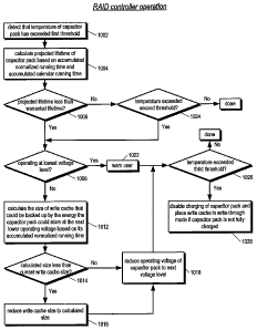
2:1 RO 0 FLUSH_STATUS Provides status of data flush operation.
00 - No Data Flush
01 - Data Flush in-progress
10 - Data Flush Completed with Errors (ECC, ATA, or
Aborted)
11 - Data Flush Completed Successfully
0 RW 0 FLUSH_START Writing "1" to this register initiates data flush
operation.
The external PWR STATE pins will also set this bit.
When the flush is complete, this bit will reset back to 0.
Writing "0" while the flush is going aborts the operation
(aborts on next 512 byte boundary). After an abort the
ATA device may need to be reset as it is left in an
unknown state.
Table 3- NV.B_FLUSH CTRL Register
[0064] The NVB RESTORE CTRL Register 304 provides the CPU subsystem 112
the ability to initiate a restore operation from non-volatile memory 108 to
cache
memory 104, and provides the CPU subsystem 112 the ability to read the status
of a
restore operation.
Bits R/W Reset Name Description
31:3 RO 0 Reserved
2:1 RO 0 RESTORE_STATUS Provides status of data restore operation.
00 - No Restore in progress
01 - Data Restore in progress
10 - Data Restore Completed with Errors (ECC,
ATA, or Aborted)
11 - Data Restore Completed without Errors
0 RW 0 RESTORE_START Writing "1" to this register initiates data restore
operation. When the restore is complete, this bit
will reset back to 0. Writing "0" while the restore
is going aborts the operation (aborts on next 512
byte boundary). After an abort the ATA device
may need to be reset as it is left in an unknown
state.
Table 4- NVB RESTORE_CTRL Register
[0065] The NVB RAM START ADDR1 Register 306 specifies the starting address
in the cache memory 104 of a first region of data that is the source or sink
of a flush
or restore operation, respectively.
Bits R/W Reset Name Description
31 RO 0 Reserved
30:9 RW 0 NVB_RAM_START_ADDRI Starting cache memory address used
for a flush or restore operation for
Region 1.
8:0 RO 0 Reserved
Table 5- NVB_RAM START ADDRl Register
CA 02622099 2008-01-24
WO 2007/018778 PCT/US2006/024660
21
[0066] The NVB ATA START ADDR1 Register 308 specifies the starting address
in the non-volatile memory 108 of the first region of data that is the sink or
source of
a flush or restore operation, respectively. In one embodiment, the memory
controller
102 converts the non-volatile memory 108 address specified in the
NVB ATA START ADDR1 Register 308 to a sector number if the non-volatile
memory 108 is a sectored ATA device.
Bits R/W Reset Name Description
31 RO 0 Reserved
30:9 RW 0 NVB_ATA_START_ADDRl Starting non-volatile memory address
used for a flush or restore operation for
Region 1.
8:0 RO 0 Reserved
Table 6- NVB ATA START ADDR1 Register
[0067] The NVB_SIZE1 Register 312 specifies the total size, or length, of the
first
region of data that is to be copied by a flush or restore operation.
Bits R/W Reset Name Description
31 RO 0 Reserved
30:9 RW 0 NVB_SIZEI Total size (length) of a flush or restore operation of
Region 1.
8:0 RO 0 Reserved
Table 7- NVB SIZE1 Register
[0068] The NVB RAM START ADDR2 Register 314 specifies the starting address
in the cache memory 104 of a second region of data that is the source or sink
of a
flush or restore operation, respectively.
Bits R/W Reset Name Description
31 RO 0 Reserved
30:9 RW 0 NVB_RAM_START_ADDR2 Starting cache memory address used
for flush or restore operation for
Region 2.
8:0 RO 0 Reserved
Table 8- NVB-RAM START ADDR2 Register
[0069] The NVB ATA START ADDR2 Register 316 specifies the starting address
in the non-volatile memory 108 of the second region of data that is the sink
or source
of a flush or restore operation, respectively. In one embodiment, the memory
controller 102 converts the non-volatile memory 108 address specified in the
NVB ATA START ADDR2 Register 316 to a sector number if the non-volatile
memory 108 is a sectored ATA device.
CA 02622099 2008-01-24
WO 2007/018778 PCT/US2006/024660
22
Bits R/W Reset Name Description
31 RO 0 Reserved
30:9 RW 0 NVB_ATA_START_ADDR2 Starting non-volatile memory address
used for a flush or restore operation
for Region 2.
8:0 RO 0 Reserved
Table 9- NVB ATA START ADDR2 Register
[0070] The NVB_SIZE2 Register 318 specifies the total size, or length, of the
second region of data that is to be copied by a flush or restore operation.
Bits R/W Reset Name Description
31 RO 0 Reserved
30:9 RW 0 NVB_SIZE2 Total size (length) of a flush or restore operation of
Region 2.
8:0 RO 0 Reserved
Table 10 - NVB_SIZE2 Register
[0071] The NVB_SECTOR COUNT Register 322 specifies the number of sectors to
use for each write/read command issued by the memory controller 102 to the non-
volatile memory 108 ATA device. The NVB_SECTOR COUNT Register 322 may
be used to optimize the speed of the flush and restore operations to and from
the non-
volatile memory 108 ATA device. The NVB_SECTOR COUNT Register 322 is
used in conjunction with the NVB_SIZE Register 312/318. For example, the CPU
subsystem 112 may program the NVB_SIZE Register 312/318 with a value of
256KB and the NVB_SECTOR COUNT Register 322 with a value of 32, resulting
in the 256KB of data being written as 16 write commands of 32 sectors (16KB)
each.
The NVB-SIZE Register 312/318 must be programmed with a value that is a
multiple of the NVB_SECTOR COUNT Register 322 value.
Bits R/W Reset Name Description
31:9 RO 0 Reserved
8:0 RW 1 NVB_SECTOR_COLJNT Non-volatile memory Sector Count.
Number of sectors to use for each
Write/Read command issued to ATA
device. The allowable values are:
Ox000 1 sector
Ox001 1 sector
0x002 2 sectors
0x004 4 sectors
0x008 8 sectors
Ox010 16 sectors
0x020 32 sectors
0x040 64 sectors
0x080 128 sectors
Ox100 256 sectors
Table 11- NVB SECTOR COUNT Register
CA 02622099 2008-01-24
WO 2007/018778 PCT/US2006/024660
23
[0072] The NVB PROGRESS Register 324 specifies the current address in the
cache memory 104 being read from or written to during a flush operation or
restore
operation, respectively. The NVB PROGRESS Register 324 is valid only when a
flush or restore operation is in progress. The NVB PROGRESS Register 324
enables the CPU subsystem 112 to assess the progress of a flush or restore
operation.
If the flush or restore operation generates an error, the NVB PROGRESS
Register
324 value specifies the approximate address where the error occurred. If a
flush or
restore operation is aborted, the NVB PROGRESS Register 324 will have
incremented to the next sector after the abort occurs.
Bits R/W Reset Name Description
31 RO 0 Reserved
30:4 RO 0 NVB_PROGRESS Current non-volatile memory flush or Restore
Address. This value is only valid during a flush
or restore operation.
3:0 RO 0 Reserved
Table 12 - NVB PROGRESS Register
[0073] The ATA INT STATUS Register 326 may be read by the CPU subsystem
112 to determine whether the non-volatile memory 108 ATA device has generated
an
interrupt, such as upon the successful read or write of one or more sectors of
data
during a flush or restore operation, and to determine whether a flush or
restore
operation has completed. The ATA INT STATUS Register 326 also enables the
CPU subsystem 112 to clear the interrupt source.
Bits R/W Reset Name Description
31:3 RO 0 Reserved
2 RO 0 ATA_DEVICE_INT ATA Device Interrupt. This bit reflects the
status of the non-volatile memory ATA
device interrupt line 1= asserted).
1 RW 1 C 0 RESTORE_DONE_INT Restore Operation Done. This bit will be set
to one when a Restore operation completes.
If the corresponding bit in the
ATA_INT_ENABLE register is also set,
then an ATA_IRQ will be generated.
Writing a one to this bit location will clear
the bit (and interrupt) as will starting a new
Restore operation.
0 RW I C 0 FLUSH_DONE_INT Flush Operation Done. This bit will be set to
one when a flush operation completes. If the
corresponding bit in the
ATA_INT_ENABLE register is also set,
then an ATA_IRQ will be generated.
Writing a one to this bit location will clear
the bit (and interrupt) as will starting a new
flush operation.
Table 13 - ATA_INT_STATUS Register
CA 02622099 2008-01-24
WO 2007/018778 PCT/US2006/024660
24
[00741 The ATA INT ENABLE Register 328 enables the CPU subsystem 112 to
enable or disable interntpt sources specified by the ATA INT STATUS Register
326.
Bits R/W Reset Name Description
31:3 RO 0 Reserved
2 RW 0 ATA_DEVICE_INT EN ATA Device Interrupt Enable. When
set to one, the ATA Device interrupt
will generate an ATA IRQ interrupt.
1 RW 0 RESTORE_DONE_INT_EN Restore Operation Done Interrupt
Enable. When set to one, the Restore
Done interrupt will generate an
ATA IR interru t
0 RW 0 FLUSH_DONE_INT_EN Flush Operation Done Interrupt Enable.
When set to one, the Flush Done
interrupt will generate an ATA_IRQ
interrupt
Table 14 - ATA INT ENABLE Register
[0075] The NVB ERROR CODE Register 332 specifies the error type when a flush
or restore operation completes if the NVB FLUSH CTRL Register 302 or
NVB RESTORE CTRL Register 304 indicates a failure. When an ECC error is
detected, the operation terminates at the next sector boundary. Consequently,
up to
512 bytes may be transferred after the error occurs. In one embodiment, the
CPU
subsystem 112 has the ability to cause ECC errors to be ignored. Hardware
detection
of ATA device errors is performed by checking the contents of the ATA Device
Status register, which is a Task File register in the ATA Direct Access
Registers 342
discussed below. The memory controller 102 reads the ATA Device Status
register
after issuing the ATA command and after the transfer of each sector completes.
Consequently, ATA device errors are detected and reported at the sector
boundary
where the error occurs, i.e., up to 512 bytes may transfer after the ATA error
actually
occurs. Likewise, ATA operations terminate only at a sector boundary.
CA 02622099 2008-01-24
WO 2007/018778 PCT/US2006/024660
Bits R/W Reset Name Description
31:9 RO 0 Reserved
8 RO 0 NVB_ERROR TYPE 0= ATA Device Error (or no error if no
failure)
1= DDR SDRAM uncorrectable error
7:0 RO 0 ATA_ERROR_CODE ATA device status register
Bit 7: BUSY
Bit 6: RDY
Bit 5: DWF - Write Fault occurred
Bit 4: DSC
Bit 3: DRQ
Bit 2: CORR
Bit 1: IDX (always 0)
Bit 0: ERR - Command ended in error
specified in ATA Device Error Task
File register
Table 15 - NVB ERROR CODE Register
[0076] The NVB_CONFIG Register 334 enables the CPU subsystem 112 to
configure aspects of a flush operation. In particular, the CPU subsystem 112
may
enable the memory controller 102 to automatically perform a flush operation or
may
disable the memory controller 102 from automatically perfonning a flush
operation.
Additionally, the CPU subsystem 112 may selectively instruct the memory
controller
102 via the NVB CONFIG Register 334 to write to the non-volatile memory 108
information specifying the results of a flush operation when the flush
operation ends,
whether the flush was successful or was aborted or an error occurred, as
described
below. The memory controller 102 writes the flush results information to a
predetermined flush results sector of the non-volatile memory 108 ATA device.
In
one embodiment, the flush results sector is the first sector of the non-
volatile
memory 108.
Bits R/W Reset Name Description
31:2 RO 0 Reserved
1 R/W 0 WR_FLUSH_RESULTS_EN Enable bit to allow the results of the
Flush Operation to be written back to
the first sector of the NVB memory.
See below for format.
0 R/W 0 AUTO_FLUSH_EN Enable bit for the Automatic Flush on
power-down. I = enabled. 0 =
disabled. If enabled, when an auto
flush operation completes (success, fail
or aborted), this bit will be cleared.
Table 16 - NVB_CONFIG Register
[0077] The ATA RESET Register 336 enables the CPU subsystem 112 to reset the
non-volatile memory 108 ATA device.
CA 02622099 2008-01-24
WO 2007/018778 PCT/US2006/024660
26
Bits R/W Reset Name Description
31:1 RO 0 Reserved
0 R/W 0 ATA_RESET When this bit is I the ATA device will be
held in reset. 0 allows normal operation.
Table 17 - ATA RESET Register
[0078] The ATA CRC Register 338 contains the 32-bit CRC for the data when a
flush or restore operation is completed. The CRC data is automatically written
to the
write results sector if the option is enabled. In one embodiment, a flush
operation
writes the CRC value to the write results sector and when a restore operation
is
performed, the CRC value is compared to the ATA CRC Register 338 value to
determine if any data corruption occurred during the flush or restore
operation,
indicated by a mismatch.
Bits R/W Reset Name Description
31:0 RO OxFFFFFFFF ATA_CRC CRC of the last Flush or Restore operation. The
CRC is a 32 bit CRC using 16 bit input. The
starting value is OxFFFFFFFF (preset). The
polynomial is:
x~32 + x~26 + x~23 + x~22 + x~ 16 + x~ 12 + x~ 11
+x~10+x~8+x~7+x~5+ x~4+x~2+x+ 1
(IEEE 802.3 CRC-32 polynomial) however, the
final result is not complemented.
Table 18 - ATA CRC Register
[0079] The format of the flush results information written to the non-volatile
memory 108 ATA device flush results sector is described in Table 19 below.
Byte Name Value
Offset
0 Completion Signature Ox13AC
2 Completion Status 0x0002 (if completion with errors or aborted)
Ox0003 (if successful com letion
4 Completion Error Code Same value as NVB ERROR CODE Register
6 High Half of CRC OxXXXX
8 Low Half of CRC OxXXXX
Reserved Ox00000000
14 Sector Pad Bytes OxFF (remainder of sector has this value)
Table 19 - Flush Results Sector Format
[0080] The Completion Signature value is also stored in the code FLASH 106 so
that
the CPU subsystem 112 can compare it with the Completion Signature in the non-
volatile memory 108 flush results sector to determine whether a flush
operation was
successful. Additionally, in one embodiment, the memory controller 102
computes a
running cyclic redundancy code (CRC) of the data as it flushes the data to the
non-
volatile memory 108, and writes the final CRC value to the flush results
sector at the
offset shown in Table 19. This enables the CPU subsystem 112 to generate a CRC
CA 02622099 2008-01-24
WO 2007/018778 PCT/US2006/024660
27
when reading the data during a restore operation to verify that the data is
valid, i.e.,
that the data was accurately written to the non-volatile memory 108 by the
flush
operation, by comparing with the ATA CRC Register 338 value.
[0081] The ATA Direct Access Registers 342 comprise control and status
registers
used by the CPU subsystem 112 to communicate with the non-volatile memory 108
ATA device. In one embodiment, the ATA Direct Access Registers 342 comprise a
standard ATA register file, commonly known as a Task File, which is well-known
in
the art of disk drives. The memory controller 102 reads and writes the ATA
Direct
Access Registers 342 to perfonn ATA commands with the non-volatile memory 108
ATA device, such as writes of posted-write data during a flush operation and
reads of
the data during a restore operation. The CPU subsystem 112 may also directly
access the ATA Direct Access Registers 342.
[0082] Referring now to Figure 4, a flowcliart illustrating operation of the
RAID
controller 100 of Figure 1 to perform a flush operation according to the
present
invention is shown. Flow begins at block 402.
[0083] At block 402, the CPU subsystem 112 programs the memory controller 102
CSRs 202 of Figure 3 with the information needed by the memory controller 102
to
perform an automatic flush operation. Preferably, the CPU subsystem 112
software
performs this function as part of its initialization sequence during boot up.
However,
in conjunction with the dynamic write cache size embodiments described herein,
the
CPU 112 may also program the memory controller 102 CSRs 202 after boot time
during normal operation of the RAID controller 100 with updated information in
response to a write cache size adjustment. In particular, the CPU subsystem
112
programs the NVB FLUSH CTRL Register 302, the NVB RAM START ADDR1
Register 306, the NVB ATA START ADDR1 Register 308, the NVB_SIZE1
Register 312, the NVB RAM START ADDR2 Register 314, the
NVB ATA START ADDR2 Register 316, the NVB_SIZE2 Register 318, the
NVB_SECTOR COUNT Register 322, the ATA INT ENABLE Register 328, and
the NVB_CONFIG Register 334 with the desired values to provide the memory
controller 102 with the necessary information to perform a flush operation. In
one
embodiment, the CPU subsystem 112 programs the memory controller 102 to flush
all cached data, i.e., posted-write data and read-cached data; however, in
another
CA 02622099 2008-01-24
WO 2007/018778 PCT/US2006/024660
28
embodiment, the CPU subsystem 112 programs the memory controller 102 to
include only posted-write data, thereby reducing the amount of energy and time
required to perform the flush operation. In addition, the CPU subsystem 112
may
initialize the flush results sector to a predetermined value in order to
enable the CPU
subsystem 112 to detennine whether the memory controller 102 successfully
wrote
the flush operation results information to the flush results sector at the end
of a flush
operation. For example, in one embodiment, the CPU subsystem 112 writes or
erases the flush results sector with a value of OxFF for each byte in the
sector. The
CPU subsystem 112 subsequently begins normal operation while the main power
source supplies power to the RAII) controller 100. Normal operation includes
performing posted write operations, causing posted-write data to be stored
into the
volatile cache memory 104. Flow proceeds to block 404.
[0084] At block 404, the main power source fails to supply power to the RAID
controller 100. In response, the capacitors 136 begin supplying power to the
predetermined portions of the RAID controller 100, namely to the cache memory
104, the non-volatile memory 108, the memory controller 102, the power manager
132, and power regulator 134 and related circuitry. In particular, the
capacitors 136
do not supply power to the CPU subsystem 112, disk interface 116, or host
interface
118. Additionally, the PCI-X interfaces 216 and 218 and FIFOs 206 that are not
needed because they are used only to interface with the disk interface 116 and
host
interface 118 are not powered by the capacitors 136. Consequently,
advantageously,
the CPU subsystem 112, disk interface 116, host interface 118 and unneeded
portions
of the memory controller 102 do not consume energy during the flush operation,
thereby enabling the RAID controller 100 to employ capacitors 136 capable of
storing less energy, which typically implies capacitors 136 that are less
expensive
and/or require less space. Additionally, the fact that the CPU subsystem 112,
disk
interface 116, and host interface 118 do not consume energy stored in the
capacitors
136 leaves more energy stored in the capacitors 136 once the flush operation
is
complete, which increases the likelihood that the capacitors 136 will continue
to
supply power to the cache memory 104 after the flush is complete thereby
keeping
the posted-write data intact, which may alleviate the need for a restore
operation
when the main power is restored, as described below. Flow proceeds to block
406.
CA 02622099 2008-01-24
WO 2007/018778 PCT/US2006/024660
29
[0085] At block 406, the power manager 132 detects the loss of main power and
commands the memory controller 102 via the pwr state signa1222 to begin a
flush
operation of data from the cache memory 104 to the non-volatile memory 108.
Flow
proceeds to block 408.
[0086] At block 408, if the AUTO FLUSH EN bit in the NVB_CONFIG Register
334 is set, then the memory controller 102 performs a flush operation based on
the
information previously programmed into the CSRs 202 at block 402. In
particular,
the memory controller 102 copies the data in the two regions specified by the
NVB RAM_START ADDR1 Register 306/NVB_SIZE1 Register 312 and
NVB RAM START ADDR2 Register 314/NVB_SIZE2 Register 318 to the two
locations in the non-volatile memory 108 specified by the
NVB ATA START ADDR1 Register 308 and NVB ATA START ADDR2
Register 316, respectively, in a manner specified by the NVB_SECTOR COUNT
Register 322 and the ATA INT ENABLE Register 328. In one embodiment, the
first region includes the portion of the posted-write data that includes the
actual user
data, and the second region includes the portion of the posted-write data that
is
metadata. In another embodiment, the first region includes the posted-write
user data
and associated metadata, and the second region includes read-cached user data
and
associated metadata. However, the use of the two regions is not limited to
these
embodiments. Furthermore, embodiments are contemplated in which the CSRs 202
include registers for specifying more or less than two data regions. Flow
proceeds to
block 412.
[0087] At block 412, if the WR FLUSH RESULTS_EN bit in the NVI3_CONFIG
Register 334 is set, then the memory controller 102 writes the flush results
information specified in Table 19 above to the flush results sector of the non-
volatile
memory 108 at the end of the flush operation, whether the flush operation was
successful, was aborted, or was terminated due to an error. If the CPU
subsystem
112 aborts a flush (or restore) operation, or if the memory controller 102
detects an
ECC or ATA error during the flush (or restore) operation, then the memory
controller 102 will terminate the flush (or restore) operation at the next
sector
boundary. If the WR FLUSH_RESULTS EN bit in the NVB CONFIG Register
334 is set, the memory controller 102 will write the flush results sector and
post a
CA 02622099 2008-01-24
WO 2007/018778 PCT/US2006/024660
Boolean 10 on the flush status signal 224 and in the FLUSH STATUS bits of the
NVB FLUSH CTRL Register 302. If, while the memory controller 102 is writing
the flush operation results to the flush results sector itself, the CPU
subsystem 112
commands an abort or the memory controller 102 detects an error, the flush
operation results may or may not be written successfully to the flush results
sector,
and if they are written, the flush results information may be unreliable. Flow
proceeds to block 414.
[0088] At block 414, after the power manager 132 commands the memory
controller
102 to initiate the flush operation, the power manager 132 monitors the
progress of
the flush operation via the flush status signal 224. When the flush operation
completes, the power manager 132 commands the memory controller 102 via the
pwr state signa1222 to place the cache memory 104 into self-refresh mode, in
order
to reduce the amount of energy stored in the capacitors 136 that is consumed
by the
cache memory 104. Flow proceeds to block 416.
[0089] At block 416, the memory controller 102 places the cache memory 104
into
self-refresh mode in response to the command performed by the power manager
132
at block 414. Flow proceeds to block 418.
[0090] At block 418, the power manager 132 causes the capacitors 136 to supply
power to the cache memory 104 only. That is, the power manager 132 causes the
capacitors 136 to no longer supply power to the non-volatile memory 108 and
the
memory controller 102, in order to reduce the amount of energy stored in the
capacitors 136 that is consumed while waiting until main power is restored.
Flow
ends at block 418.
[0091] Referring now to Figure 5, a flowchart illustrating operation of the
RAID
controller 100 of Figure 1 in response to main power being restored after a
failure of
main power according to the present invention is shown. Flow begins at block
502.
[0092] At block 502, the main power source resumes supplying power to the RAID
controller 100. Consequently, the CPU subsystem 112 software boots up and
begins
its initialization sequence. Flow proceeds to decision block 504.
[0093] At decision block 504, the CPU subsystem 112 determines whether the
cache
memory 104 contents is still valid. In one embodiment, the CPU subsystem 112
determines whether the cache memory 104 contents is still valid by examining a
data
CA 02622099 2008-01-24
WO 2007/018778 PCT/US2006/024660
31
good indicator in the power manager 132 that may be written by the memory
controller 102. The power manager 132 is configured such that when it is
powered
up, the data good indicator resets to a predetermined value, such as a Boolean
value
of zero. Furthermore, the power-off threshold of the power manager 132 is at
least
as high as the power threshold at which the cache memory 104 begins to lose
its data.
When main power is lost, the memory controller 102 writes a value into the
data
good indicator different from the power-up reset value. Thus, if the
capacitors 136
fail to supply power to the cache memory 104 (and therefore also fail to
supply
power to the data good indicator), when main power is restored, the CPU
subsystem
112 will read the power-up reset value from the data good indicator rather
than the
value written by the memory controller 102. Consequently, the CPU subsystem
112
will determine that the cache memory 104 must be restored from the non-
volatile
memory 108, if the flush operation was successful. However, if the CPU
subsystem
112 reads from the data good indicator the value written by the memory
controller
102, then the CPU subsystem 112 will determine that it can forego restoring
the
cache memory 104 thereby making the user data available to the host computers
sooner. If the cache memory 104 contents is still valid, flow proceeds to
decision
block 516; otherwise, flow proceeds to decision block 506.
[0094] At decision block 506, the CPU subsystem 112 determines whether a flush
operation performed according to Figure 4 was successfully completed by
examining
the FLUSH STATUS bits of the NVB FLUSH CTRL Register 302. In one
embodiment, the CPU subsystem 112 additionally determines whether the flush
operation completed successfully by examining the Completion Status in the
flush
results sector. In one embodiment, the CPU subsystem 112 additionally
determines
whether the flush operation completed successfully by comparing the Completion
Signature in the flush results sector with the Completion Signature in the
code
FLASH 106. In one embodiment, the CPU subsystem 112 additionally determines
whether the flush operation completed successfully by comparing the CRC in the
flush results sector with the CRC computed by reading the data from the non-
volatile
memory 108. If the flush operation completed successfully, flow proceeds to
block
512; otherwise, flow proceeds to block 508.
CA 02622099 2008-01-24
WO 2007/018778 PCT/US2006/024660
32
[0095] At block 508, since the posted-write data has been lost, the RAID
controller
100 fails over to the partner, i.e., redundant, RAID controller 100 in the
system. In
one embodiment, during normal operation when a host issues a write I/O request
to
the RAID controller 100, the posted write data is also written to the partner
RAID
controller 100. Consequently, if one of the RAID controllers 100 fails, in
particular
if a flush operation fails on one RAID controller 100, there is a high
probability that
the flush operation succeeded on the partner RAID controller 100. If so, the
partner
RAID controller 100 can perform a restore of the posted-write data from its
non-
volatile memory 108 to the cache memory 104 and subsequently flush the posted-
write data to disk. Flow ends at block 508.
[0096] At block 512, the CPU subsystem 112 commands the memory controller 102
to perform a restore operation to restore the data flushed from the cache
memory 104
to the non-volatile memory 108 during the flush operation described in Figure
4 back
to the cache memory 104. Prior to commanding the memory controller 102 to
perform the restore operation, the CPU subsystem 112 programs the appropriate
values into the various CSRs 202 of the memory contro]ler 102 needed to
perform
the restore operation. In one embodiment, the CPU subsystem 112 performs the
restore operation, rather than commanding the memory controller 102 to perform
the
restore operation, by simply reading data from the non-volatile memory 108 and
writing the data to the cache memory 104. Because the restore operation is
performed while the main power source is supplying power, it is not as crucial
that
the memory controller 102 perform the restore operation at a lower power
consumption level. However, this embodiment has the disadvantage that the CPU
subsystem 112 may take longer than the memory controller 102 to complete the
restore operation. Flow proceeds to block 514.
[0097] At block 514, the CPU subsystem 112'flushes the posted-write data from
the
cache memory 104 to disk. Flow ends at block 514.
[0098] At decision block 516, the CPU subsystem 112 determines whether a flush
operation is in progress by reading the FLUSH STATUS bits of the
N'VB FLUSH CTRL Register 302. If a flush operation is in progress, flow
proceeds to decision block 518; otherwise, flow proceeds to block 514.
CA 02622099 2008-01-24
WO 2007/018778 PCT/US2006/024660
33
[0099] At decision block 518, the CPU subsystem 112 examines the capacitors
136
voltage level to determine whether the voltage level is above a minimum
threshold.
In one embodiment, the minimum voltage threshold value is programmed into the
CPU subsystem 112 software. In another embodiment, the minimum voltage
threshold value is user-programmable via a user configuration program. If the
capacitors 136 voltage level is above the minimum threshold, flow returns to
decision block 516 to wait until either the flush operation completes or the
capacitors
136 voltage reaches the minimum threshold; otherwise, flow proceeds to block
522.
[00100] At block 522, the CPU subsystem 112 aborts the flush operation by
writing a Boolean 0 to the FLUSH START bit in the NVB FLUSH CTRL Register
302. Flow proceeds to block 514.
[00101] The process of waiting to boot the RAID controller 100 and resume
normal operations if the cache memory 104 is still good and a flush operation
is in
progress until either the flush completes or the capacitors 136 voltage level
reaches
the minimum threshold solves the problem which might exist without the benefit
of
the additional test at decision block 518, as exemplified by the following
sequence of
events. Assume the power manager 132 senses the loss of main power and
commands the memory controller 102 to perform a flush operation. A significant
amount of the capacitors 136 stored energy is consumed by the flush operation.
Before the flush operation completes, main power is restored; consequently,
the CPU
subsystem 112 aborts the flush operation. T'he CPU subsystem 112 boots up and
enables another flush operation in the event of another main power loss.
Shortly
thereafter, and significantly, while the capacitors 136 are less than fully re-
charged,
the power manager 132 senses another loss of main power and commands the
memory controller 102 to perform another flush operation. The second flush
operation consumes again a significant amount of the capacitors 136 stored
energy,
which began with less than a full charge. If this sequence continues,
eventually the
capacitors 136 will not have enough energy to complete a successful flush
operation,
resulting in potential loss of user data. The scenario described above may be
induced
by periodic brown-outs of the main power supply or possibly by a noisy power
supply that cause the power manager 132 to sense that main power is being lost
in a
relatively periodic fashion in which the period is on the order of the flush
operation
CA 02622099 2008-01-24
WO 2007/018778 PCT/US2006/024660
34
time. However, advantageously, the additional test at decision block 518
potentially
avoids this problem. In an alternate embodiment, the write cache 156 is placed
in
write-through mode since the capacitor pack 136 is not fully charged thereby
avoiding the undesirable scenario. In another alternate embodiment, at block
518 the
CPU 112 determines whether the flush operation is complete and if so flow
proceeds
to block 514; otherwise, flow returns to block 516.
[00102] Although embodiments have been described in which the memory
controller is employed to perform the posted-write data flush from volatile
memory
to non-volatile memory, embodiments are contemplated in which the CPU performs
the flush from volatile memory to non-volatile memory, as illustrated in
Figures 6
and 7. The embodiment of Figures 6 and 7 which use the CPU subsystem 112 to
perform the flush operation may be a viable embodiment if one or more of the
following in combination is true: the energy density of the capacitors 136 is
sufficiently high to store the energy needed by the RAID controller 100,
including
the CPU subsystem 112, to perform the flush operation; the available space
allocated
for the capacitors 136 on the RAID controller 100 is sufficiently great to use
enough
capacitors 136 to store the energy needed by the RAID controller 100,
including the
CPU subsystem 112, to perform the flush operation; the CPU subsystem 112
consumes a small enough amount of power such that the capacitors 136 can store
the
energy needed by the RAID controller 100, including the CPU subsystem 112, to
perform the flush operation. Although this embodiment may consume more energy
than the embodiments described in Figures 1 through 5, if the capacitors 136
are able
to supply the required energy, then the RAID controller 100 would enjoy the
benefits
of capacitor technology over battery technology described herein, such as
lower cost,
higher reliability, less maintenance, and shorter re-charge time.
[00103] Referring now to Figure 6, a block diagram illustrating a RAID
controller 600 according to an alternate embodiment of the present invention
is
shown. The RAID controller 600 of Figure 6 is similar to the RAID controller
100
of Figure 1; however, the power manager 132 is coupled to communicate with the
CPU subsystem 112 with respect to flush operations rather than to the memory
controller 102, as shown, and as described with respect to Figure 7.
CA 02622099 2008-01-24
WO 2007/018778 PCT/US2006/024660
[00104] Referring now to Figure 7, a flowchart illustrating operation of the
RAID controller 600 of Figure 6 to perform a flush operation according to an
alternate embodiment of the present invention is shown. Flow begins at block
704.
[00105] At block 704, the main power source fails to supply power to the
RAID controller 600. In response, the capacitors 136 begin supplying power to
the
predetermined portions of the RAID controller 600, namely to the cache memory
104, the non-volatile memory 108, the memory controller 102, the power manager
132, power regulator 134, CPU subsystem 112, and related circuitry. In
particular,
the capacitors 136 do not supply power to the disk interface 116, or host
interface
118. Additionally, the PCI-X interfaces 216 and 218 and FIFOs 206 that are not
needed because they are used only to interface with the disk interface 116 and
host
interface 118 are not powered by the capacitors 136. Consequently,
advantageously,
the disk interface 116, host interface 118 and unneeded portions of the memory
controller 102 do not consume energy during the flush operation, thereby
enabling
the RAID controller 100 to employ capacitors 136 capable of storing less
energy,
which typically implies capacitors 136 that are less expensive and/or require
less
space. Additionally, the fact that the disk interface 116 and host interface
118 do not
consume energy stored in the capacitors 136 leaves more energy stored in the
capacitors 136 once the flush operation is complete, which increases the
likelihood
that the capacitors 136 will continue to supply power to the cache memory 104
after
the flush is complete thereby keeping the posted-write data intact, which may
alleviate the need for a restore operation when the main power is restored, as
described below. Flow proceeds to block 706.
[00106] At block 706, the power manager 132 detects the loss of main power
and notifies the CPU subsystem 112 that a flush operation of data from the
caclie
memory 104 to the non-volatile memory 108 is needed. Flow proceeds to block
708.
[00107] At block 708, the CPU subsystem 112 performs a flush operation by
copying the data from the cache memory 104 to the non-volatile memory 108.
Flow
proceeds to block 712.
[00108] At block 712, the CPU subsystem 112 writes the flush results
information specified in Table 19 above to the flush results sector of the non-
volatile
memory 108 upon completion of the flush operation, whether the flush operation
was
CA 02622099 2008-01-24
WO 2007/018778 PCT/US2006/024660
36
successful, was aborted, or was tenninated due to an error. Flow proceeds to
block
716.
[00109] At block 716, the CPU subsystem 112 places the cache memory 104
into self-refresh mode. Flow proceeds to block 718.
[00110] At block 718, the CPU subsystem 112 commands the power manager
132 to cause the capacitors 136 to supply power to the cache memory 104 only.
That
is, the power manager 132 causes the capacitors 136 to no longer supply power
to the
CPU subsystem 112, non-volatile memory 108 and the memory controller 102, in
order to reduce the amount of energy stored in the capacitors 136 that is
consumed
while waiting until main power is restored. Flow ends at block 718.
[00111] Referring now to Figure 8, a block diagram illustrating a table 800,
or
database 800, for storing lifetimes of the capacitor pack 136 of Figure 1 for
various
temperature and voltage combinations according to the present invention is
shown.
The values indicated in Figure 8 are hypothetical values provided for
illustration
purposes, and do not represent actual known values of a particular capacitor
product,
which may be obtained from the capacitor manufacturer. Furthermore, the range
of
temperatures shown is a hypothetical range selected for illustration purposes.
[00112] As explained above, the purpose of the capacitor pack 136 is to store
energy to supply power for backing up, or flushing, the write cache data from
the
write cache 156 to the non-volatile memory 108 in response to a main power
loss.
When the capacitor pack 136 no longer has the capacity to store sufficient
energy to
backup the write cache 156 to the non-volatile memory 108, the capacitor pack
136
has reached its end of life, i.e., its lifetime has expired. The capacitance
of the
capacitor pack 136 drops over time as the capacitor pack 136 is used in
operation of
the RAID controller 100. Various factors affect the capacitance drop of the
capacitor
pack 136, including the temperature, the operating voltage, excessive current
draws,
and changes in polarity of the capacitor pack 136. In one embodiment, the
current
draw of the capacitor pack 136 is monitored also, and if the current draw
exceeds a
predetermined amount, charging of the capacitor pack 136 is temporarily
disabled to
avoid prematurely reducing the lifetime of the capacitor pack 136, as
discussed
below. The polarity of the capacitor pack 136 is kept the same during
operation of
the RAID controller 100 to avoid prematurely reducing the lifetime of the
capacitor
CA 02622099 2008-01-24
WO 2007/018778 PCT/US2006/024660
37
pack 136. Thus, the primary factors affecting the capacitor pack 136
capacitance,
and thus lifetime, are the temperature and operating voltage.
[00113] In one embodiment of the RAID controller 100, the warranted lifetime
of the capacitor pack 136 is 5 years. That is, the RAID controller 100
manufacturer
warrants that the capacitor pack 136 will have sufficient capacitance for at
least 5
years to store sufficient energy to backup the write cache 156 to the non-
volatile
memory 108. The amount of energy each capacitor in the capacitor pack 136 is
capable of storing is given by equation (1), where E is the energy stored by
the
capacitor, C is the capacitance of the capacitor, Vop is the operating voltage
of the
capacitor and VIõin is the cut-off voltage of the capacitor:
E = 1/2 * C * (Vop2 - Vmin2) (1)
In one embodiment, the capacitor pack 136 is arranged as four capacitors in
series,
each capacitor being of the same type. Thus, the total energy stored by the
capacitor
pack 136 is the sum of the energy stored by each of the four capacitors in the
capacitor pack 136, or approximately four times the energy stored by a single
capacitor in the pack. Furthermore, the operating voltage of the capacitor
pack 136
is the sum of the operating voltage of the four capacitors in the capacitor
pack 136, or
approximately four times the operating voltage of a single capacitor in the
pack. The
RAID controller 100 includes an active balance equalizer circuit that employs
a quad
operational amplifier circuit to balance the voltage across each capacitor of
the
capacitor pack 136 to be approximately one-fourth of the total capacitor pack
136
voltage. In one embodiment, it is assumed that the ambient temperature and
operating voltage of each of the individual capacitors in the capacitor pack
136 is
approximately the same; consequently, the lifetime of each of the individual
capacitors is approximately the same. Another embodiment is contemplated in
which the lifetime of each individual capacitor in the capacitor pack 136 is
calculated
based on the temperature and individual voltage readings, and the lifetime of
the
capacitor with the lowest computed lifetime limits the lifetime of the
capacitor pack
136 as a whole.
[00114] In one embodiment, the end of life for the capacitor pack 136 is
chosen to be the condition when the individual capacitors of the capacitor
pack 136
have suffered a 30% capacitance drop from their original capacitance value. In
one
CA 02622099 2008-01-24
WO 2007/018778 PCT/US2006/024660
38
embodiment, once the 30% capacitance drop is reached, the capacitor pack 136
is no
longer capable of storing sufficient energy to perform the backup at the
normal
operating voltage. In another embodiment, the 30% capacitance drop end of life
value is chosen to provide some margin for error; that is, the capacitors in
the
capacitor pack 136 may actually have to suffer more than the 30% capacitance
drop
in order to no longer be capable of storing sufficient energy to perform the
backup at
the normal operating voltage. The 30% capacitance drop value is used herein to
illustrate the invention. However, it should be understood that the invention
is not
limited to a particular capacitance drop value; rather, the invention may be
practiced
with other capacitance drop values depending upon the amount of energy
required to
perform the backup and the characteristics of the particular capacitors
employed.
The lifetime values specified in the table 800 of Figure 8 indicate the number
of
hours that an individual capacitor of the capacitor pack 136 may operate at
the
specified temperature and voltage before reaching its end of life percentage
capacitance drop from its original capacitance value. Thus, each lifetime
value
stored in the table 800 may be understood as specifying a lifetime over wliich
the
capacitor pack 136 would have a capacity to store at least a predetermined
amount of
energy if the capacitor pack 136 were operated at the indexed temperature and
voltage during the lifetime specified. In one embodiment, the predetermined
amount
of energy is the calculated amount of energy required to supply sufficient
energy to
backup the full size write cache 156 to the non-volatile memory 108.
[00115] In one embodiment, the table 800 of Figure 8 is stored as a two-
dimensional array in the code FLASH 106 and copied to the program RAM of the
CPU subsystem 112 when the RAID controller 100 is booted so that the CPU 112
can lookup lifetimes in the table 800 using sampled temperature and voltage
values.
In the embodiment of Figure 8, the RAID controller 100 supports operating the
capacitor pack 136 at two different voltages, 8.2V and 7.2V, as shown in the
table
800. In the table 800, the 8.2V operating voltage occupies index 0 of the
array, and
the 7.2V operating voltage occupies index 1 of the array. Advantageously,
described
herein is a method for dynamically reducing, or throttling, the operating
voltage of
the capacitor pack 136 to the lower voltage level if necessary, in order to
increase the
lifetime of the capacitor pack 136. Although the embodiment of Figure 8
illustrates
CA 02622099 2008-01-24
WO 2007/018778 PCT/US2006/024660
39
only two possible operating voltages, the invention is not limited to two
operating
voltages; rather, embodiments with a larger number of operating voltages are
contemplated. Furthermore, embodiments with operating voltage values other
than
those illustrated are contemplated. In the exemplary embodiment, four
capacitors
136 are arranged in series, and each capacitor 136 operates at approximately
2.05V
or 1.8V, depending upon the capacitor pack 136 operating voltage controlled by
the
CPU 112. The array 800 comprises two columns corresponding to the two
voltages.
The rows of the array 800 are indexed by the temperature value. Each row
corresponds to a different integer degree Celsius value. The table 800 of the
embodiment of Figure 8 includes ambient temperature values from 10 degrees
Celsius to 40 degrees Celsius. For example, the lifetime at 40 degrees Celsius
and
8.2V (or 2.05V per capacitor) is 800 hours and at 7.2V (or 1.8V per capacitor)
is 820
hours, as shown in Figure 8. In one embodiment, assuming a fixed operating
voltage
value, the characteristics of the capacitors in the capacitor pack 136 are
such that the
lifetime values approximate a logarithmic function of the temperature. The CPU
112
uses the sampled temperature and voltage values to index the table 800 to
obtain the
specified lifetime in order to calculate the accumulated normalized running
time 152
and related values, as described below with respect to the remaining Figures.
[00116] As discussed above, in one embodiment, the warranted lifetime is 5
years. However, for the sake of discussion with respect to the hypothetical
values of
table 800, assume a warranted lifetime of 1000 hours. As may be observed from
table 800, if the capacitor pack 136 were continuously operated at 8.2V and 25
degrees Celsius, it would have a lifetime of the warranted 1000 hours, i.e.,
it would
reach its end of life percentage capacitance drop (e.g., 30%) after 1000
hours. In
contrast, if the capacitor pack 136 was continuously operated at 7.2V and 28
degrees
Celsius, it would have a lifetime of the warranted 1000 hours, i.e., it would
reach its
end of life capacitance drop after 1000 hours. Thus, the "normal" temperature
when
operating the capacitor pack 136 at 8.2V is 25 degrees, and the "normal"
temperature
when operating at 7.2V is 28 degrees. That is, the normal temperature, for a
given
operating voltage, is the temperature at wliich the capacitor pack 136
lifetime meets
the warranted lifetime, or exceeds the warranted lifetime where margin is
desired.
However, whereas the values of the table 800 may be derived experimentally in
CA 02622099 2008-01-24
WO 2007/018778 PCT/US2006/024660
laboratory conditions in which the temperature and voltage of the capacitors
are
maintained at constant values, when the capacitor pack 136 is operating within
the
RAID controller 100 within a computer system, the temperature will vary from
the
normal temperature. Similarly, advantageously the operating voltage of the
capacitor
pack 136 may be purposely dynamically adjusted when necessary in order to
increase the lifetime of the capacitor pack 136 to attempt to provide the
warranted
lifetime, as described below. Thus, advantageously, the present invention
describes
how the RAID controller 100 normalizes the lifetime values obtained from the
table
800 relative to the normal temperature for the particular operating voltage
level, as
described below with respect to Figure 9.
[00117] In one embodiment, the capacitor pack 136 includes four 50 Farad
capacitors in series storing approximately 356 Joules of usable energy when
fully
charged and at full capacitance, assuming a 2.05V operating voltage of each
capacitor and a 0.8V cut-off voltage, which defines the minimum working
voltage
for reliable FET gate thresholds and low drop out regulation; in contrast, at
a 30%
capacitance drop, the capacitor pack 136 is capable of storing only 250
Joules. The
capacitor pack 136 is capable of storing 260 Joules of usable energy assuming
a 1.8V
operating voltage of each capacitor; in contrast, at a 30% capacitance drop,
the
capacitor pack 136 is capable of storing only 182 Joules. In one embodiment,
the
power consumption of the cache memory 104, non-volatile memory 108, meinory
controller 102, power manager 132, DDR-SDRAM bus interface termination
circuitry, a clocking circuit, and other miscellaneous circuitry requiring
power during
the flush operation is approximately 4 Watts. The non-volatile memory 108 is
capable of being written to at a sustained rate of approximately 10MB/second.
In
one embodiment, the size of the cache memory 104 is 1GB, which comprises
approximately 512MB for a full size write cache 156, and the size of the non-
volatile
memory 108 is 512MB. Consequently, the flush operation takes approximately 50
seconds to complete and consumes approximately 200 Joules of energy. Tlius, as
may be observed, when the capacitor pack 136 is operating at the lower 7.2V
level,
even before capacitor pack 136 reaches the 30% capacitance drop end of life,
the
capacitor pack 136 may not be able to store sufficient energy to backup the
entire
write cache 156. Advantageously, described herein is a method for dynamically
CA 02622099 2008-01-24
WO 2007/018778 PCT/US2006/024660
41
reducing the write cache 156 to a size for which the capacitor pack 136 can
supply
enough energy to perform the backup.
[00118] Although embodiments are described herein in which the warranted
lifetime is based on a predetermined amount of energy required to perform the
write
cache 156 to non-volatile memory 108 backup, the capacitor pack 136 lifetime
monitoring and dynamic voltage throttling methods described herein are not
limited
to such an application. Rather other embodiments are conteinplated in which
the
warranted lifetime is based on a predetermined amount of energy required to
perform
other functions. For example, embodiments are contemplated in whicli the RAID
controller 100 does not include a non-volatile memory 108 for backing up the
write
cache 156, and the predetermined amount of energy is an amount of energy
required
to supply power to the volatile memory 104 for a predetermined amount of time,
e.g.,
3 days, during loss of main power in order to retain the integrity of the data
in the
write cache 156 until main power can be restored.
[00119] Referring now to Figure 9, a flowchart illustrating operation of the
RAID controller 100 of Figure 1 according to the present invention is shown.
In
particular, Figure 9 illustrates how the RAID controller 100 calculates the
accumulated normalized running time 152 of the capacitor pack 136. Flow begins
at
block 902.
[00120] At block 902, the CPU 112 initializes the accumulated normalized
running time 152 and accumulated calendar running time 154. In one embodiment,
the accumulated normalized running time 152 and accumulated calendar running
time 154 are initialized when the RAID controller 100 is manufactured. In one
embodiment, the accumulated normalized running time 152 and accumulated
calendar running time 154 are initialized to zero. In another embodiment, the
accumulated normalized running time 152 and accumulated calendar running time
154 are initialized to an amount of time based on the tolerance factor of the
capacitance value of the capacitor pack, such as specified by the manufacturer
of the
capacitor pack. For example, if the capacitor manufacturer specifies a 10%
tolerance, then the accumulated normalized running time 152 and accumulated
calendar running time 154 are initialized to 10% of the end of life value,
e.g., 10% of
years. In another embodiment, the accumulated normalized running time 152 and
CA 02622099 2008-01-24
WO 2007/018778 PCT/US2006/024660
42
accumulated calendar running time 154 are initialized to a calendar age, such
as the
amount of time since the manufacture of the capacitor pack 136. Other
embodiments
are contemplated in which the accumulated normalized running time 152 and
accumulated calendar ranning time 154 are initialized to a value based on a
combination of tolerance value and calendar age. Other embodiments are
contemplated in which the accumulated normalized running time 152 and
accumulated calendar running time 154 are initialized to a value based on a
desired
margin of error. Flow proceeds to block 904.
[00121] At block 904, the CPU 112 periodically samples the temperature and
voltage of the capacitor pack 136 via the temperature sensors 142 and voltage
sensors 144, respectively, of Figure 1 over a larger time interval and
averages the
sampled temperature and voltage. In one embodiment, the sample period is 15
seconds and the averaging interval is one hour. Advantages of averaging the
sampled values over a larger interval and writing the accumulated normalized
running time 152 and accumulated calendar running time 154 to the non-volatile
memory 108 once per the larger interval time, rather than each time the values
are
sampled, are that it reduces the amount of CPU 112 bandwidth consumed and
potentially avoids exceeding the maximum number of write cycles to the non-
volatile
memory 108. Flow proceeds to block 906.
[00122] At block 906, the CPU 112 looks up the lifetime at the averaged
temperature and voltage of block 904 by indexing the table 800 of Figure 8 to
obtain
the lifetime for the averaged temperature and voltage. In one embodiment, the
averaged temperature and voltage values are rounded up to the next highest
value if
necessary. For example, if the average temperature is 30.8 degrees, then the
value is
rounded up to 31 degrees for use as ati index into the table 800 of Figure 8.
Similarly, if the average sampled voltage is 7.8V, then the value is rounded
up to
8.2V and the voltage index into the table 800 is 0. It is noted that in an
altexnate
embodiment, if the lifetime values are susceptible to being expressed by a
function of
temperature and voltage, the lifetime values may be calculated from the
function
rather than looked up in the table 800. A potential disadvantage of this
embodiment
is that it may require of the CPU 112 more computation bandwidth, in
particular to
perform floating point computations, than the table lookup method. However, a
CA 02622099 2008-01-24
WO 2007/018778 PCT/US2006/024660
43
potential advantage of this embodiment is that it may enable a fmer
granularity of
temperature and voltage values than the lookup table method. Flow proceeds to
block 908.
[00123] At block 908, the CPU 112 normalizes the interval by multiplying the
interval by the ratio of the warranted lifetime to the lifetime value obtained
at block
906. For example, assume the interval is one hour, the warranted lifetime is
1000
hours, and the lifetime obtained at block 906 is 2000 hours (because the
measured
temperature and/or voltage are below the normal temperature and voltage), then
the
normalized interval would be 1 hour * (1000 / 2000) = 0.5 hours; thus, the
normalized interval is less than the calendar time of the interval, thereby
indicating
that effectively less than one hour of the capacitor pack 136 lifetime was
reduced
during the one hour calendar operating interval. In contrast, assume the
lifetime
obtained at block 906 is only 500 hours (because the measured temperature
and/or
voltage are above the normal temperature and voltage), then the normalized
interval
would be 1 hour * (1000 / 500) = 2 hours; thus, the normalized interval is
more than
the calendar time of the interval, thereby indicating that effectively more
than one
hour of the capacitor pack 136 lifetime was reduced during the one hour
calendar
operating interval. Flow proceeds to block 912.
[00124] At block 912, the CPU 112 adds the normalized interval calculated at
block 908 to the accumulated normalized running time 152 to produce an updated
accumulated normalized running time 152 value reflecting the effect of
operating the
capacitor pack 136 at the average temperature and voltage obtained at block
904 over
the interval of block 904. Additionally, the CPU 112 adds the averaging
interval
(i.e., the non-normalized interval, e.g., one hour) to the accumulated
calendar
running time 154 to produce an updated accumulated calendar rurming time 154
value. Flow proceeds to block 914.
[00125] At block 914, the CPU 112 writes the updated accumulated
normalized running time 152 and accumulated calendar running time 154
calculated
at block 912 to the non-volatile memory 108 so that their values may be
maintained
tlirough a loss of main power and subsequently used again after the RAID
controller
100 is rebooted. Flow proceeds to block 916.
CA 02622099 2008-01-24
WO 2007/018778 PCT/US2006/024660
44
[00126] At block 916, the CPU 112 calculates the percent of nonnalized
warranted lifetime used as the ratio of the accumulated normalized running
time 152
to the warranted lifetime. For example, if the accumulated normalized rumling
time
152 is 200 hours and the warranted lifetime is 1000 hours, then the percent of
normalized warranted lifetime used of the capacitor pack 136 is 20%, i.e.,
effectively
20% of the warranted lifetime has been used up, and effectively 800 hours of
lifetime
remain. Flow proceeds to block 918.
[00127] At block 918, the CPU 112 calculates the percentage capacitance drop
of the capacitor pack 136 as the product of the percent of normalized
warranted
lifetime used calculated at block 916 and the end of life capacitance drop
percentage.
For example, if the end of life capacitance drop percentage is 30%, and the
percent of
normalized warranted lifetime used calculated at block 916 is 20%, then the
percentage capacitance drop of the capacitor pack 136 is 6%. Flow proceeds to
block 922.
[00128] At block 922, the CPU 112 reports the percentage capacitance drop of
the capacitor pack 136 calculated at block 918 to the user. Furthermore, the
user is
informed whether the percentage capacitance drop is in a good, warning, or
failed
range. In one embodiment, once the percentage capacitance drop is within 1% of
the
end of life percentage capacitance drop, the user is warned that the end of
life is
approaching. In one embodiment, the user may input the range in which to be
notified that the end of life is approaching. In one embodiment, the user is
also
informed of the end of life capacitance drop percentage for comparing against
the
percentage capacitance drop. In one embodiment, the CPU 108 also reports to
the
user the remaining number of normalized lifetime hours calculated as the
warranted
lifetime minus the accumulated normalized running time 152. In one embodiment,
the temperature and voltage of the capacitor pack 136 as well as the voltage
of each
capacitor in the capacitor pack 136 is reported to the user. In one
embodiment, the
information is provided to the user via a serial interface. In one embodiment,
the
information is provided to the user via a web browser interface, such as via a
TCP/IP
connection over an Ethernet interface. Flow returns to block 904 to monitor
the
capacitor pack 136 lifetime for another interval.
CA 02622099 2008-01-24
WO 2007/018778 PCT/US2006/024660
[00129] As may be observed from Figure 9, the RAID controller 100
advantageously calculates the accumulated normalized running time 152, which
is
effectively a measure of the age, or life, of the capacitor pack 136 relative
to its
warranted lifetime. In contrast to the accumulated calendar running time 154
which
is a sum of the calendar time intervals over which the capacitor pack 136 is
operated,
the accumulated normalized running time 152 is a sum of normalized running
times
corresponding to the calendar time intervals that constitute the accumulated
calendar
running time 154. The normalized running times are calculated by normalizing
the
lifetime reading of table 800 for the average sampled temperature during the
interval
relative to the normal temperature at the average sampled operating voltage
during
the interval. Thus, the accumulated normalized running time 152 provides a
more
meaningful and accurate measure of the effective age of the capacitor pack 136
than
the calendar age of the capacitor pack 136, and does so without suffering the
detrimental performance impact associated witli the discharging/recharging
method
of measuring the capacitance of the capacitor pack 136.
[00130] It is noted that in the embodiment described in Figure 9, the
accumulated normalized running time 152 and accumulated calendar running time
154 are only updated during operation of the RAID controller 100, and in
particular,
during operation of the CPU 112. In particular, these values are not updated
when
the entire RAID controller 100 is powered off and when the CPU 112 is powered
off
during a write cache 156 backup to non-volatile memory 108, wliich would be
true in
the embodiment of Figure 1 (although not in the embodiment of Figure 5).
However,
it is noted that when the RAID controller 100 is powered off, the charge on
the
capacitor pack 136 will typically drain relatively quickly, thereby reducing
the
voltage; and, at lower voltages the capacitor pack 136 ages very slowly. Thus,
the
powered-off time is likely not significant relative to embodiments with a
warranted
lifetime on the order of 5 years; however, in an embodiment in which the
warranted
lifetime is significantly less, the powered-off time may be taken into
account. This is
in contrast to batteries, whose ability to store energy degrades significantly
during
non-use. Furthermore, the amount of time required to perform the backup is on
the
order of minutes. Thus, the backup time, even if normalized at a higlier
temperature,
is likely not significant relative to embodiments with a warranted lifetime on
the
CA 02622099 2008-01-24
WO 2007/018778 PCT/US2006/024660
46
order of 5 years; however, in an embodiment in which the warranted lifetime is
significantly less, the backup time may be taken into account.
[00131] Referring now to Figure 10, a flowchart illustrating operation of the
RAID controller 100 of Figure 1 according to the present invention is shown.
In
particular, Figure 10 illustrates how the RAID controller 100 throttles the
operating
voltage of the capacitor pack 136 to extend the accumulated normalized running
time
152 of the capacitor pack 136 when necessary. Figure 10 also illustrates how
the
RAID controller 100 dynamically reduces the write cache 156 size when
necessary.
Flow begins at block 1002.
[00132] At block 1002, the CPU 112 detects that the temperature of the
capacitor pack 136 has exceeded a first predetermined threshold. In one
embodiment, the first predetermined threshold is 51 degrees Celsius. Although
Figure 10 discloses an embodiment in which the operating voltage of the
capacitor
pack 136 is throttled and the write cache 156 size is adjusted in response to
detecting
that the capacitor pack 136 temperature has exceeded a threshold, the voltage
throttling and write cache 156 size adjustment methods described herein are
not
limited to this embodiment; rather, other embodiments are contemplated in
which the
RAID controller 100 throttles the operating voltage and adjusts the write
cache 156
size for other reasons. For example, in one embodiment, at the end of each
interval
of Figure 9, when the CPU 112 calculates the accumulated normalized running
time
152 and accumulated calendar running time 154, the CPU 112 proceeds to block
1004 to determine whether voltage throttling and/or write cache 156 size
adjustment
is necessary. For another example, although the temperature of the capacitor
pack
136 may not have risen above the first threshold, the RAID controller 100 may
determine that the capacitor pack 136 is reaching the end of its life and give
the user
the option of continuing to operate instead replacing the RAID controller 100,
albeit
at a smaller write cache 156 size. Flow proceeds to block 1004.
[00133] At block 1004, the CPU 112 calculates the projected lifetime of the
capacitor pack 136 based on the accumulated normalized running time 152 and
the
accumulated calendar running time 154. In particular, the projected lifetime
is
calculated as the product of the warranted lifetime and the ratio of the
accumulated
calendar running time 154 to the accumulated normalized running time 152. For
CA 02622099 2008-01-24
WO 2007/018778 PCT/US2006/024660
47
example, if the warranted lifetime is 1000 hours, the accumulated calendar
running
time 154 is 300 hours, and the accumulated normalized running time 152 is 200
hours, then the projected lifetime is 1000 hours * (300 / 200) = 1500 hours.
Flow
proceeds to decision block 1006.
[00134] At decision block 1006, the CPU 112 compares the projected lifetime
of the capacitor pack 136 calculated at block 1004 with the warranted lifetime
to
determine whether the projected lifetime is less than the warranted lifetime.
If so,
flow proceeds to decision block 1008; otherwise, flow proceeds to decision
block
1024.
[00135] At decision block 1008, the CPU 112 determines whether the
capacitor pack 136 is already currently operating at the lowest voltage level.
In the
example in which only two voltage levels are provided (e.g., 8.2V and 7.2V),
then
the lowest voltage level is 7.2V. However, other embodiments are contemplated
in
which more than two voltage levels are provided. An advantage of providing
more
voltage levels is that the fmer granularity may enable fmer granularity
adjustments of
the write cache 156; however, a disadvantage is that it potentially requires
more
complex voltage adjustment circuitry and software for making the voltage
adjustments and write cache 156 size adjustments. If the capacitor pack 136 is
already currently operating at the lowest voltage level, then flow proceeds to
block
1022; otherwise, flow proceeds to block 1012.
[00136] At block 1012, the CPU 112 has determined that the capacitor pack
136 operating voltage must be reduced, so the CPU 112 calculates the size of
the
write cache 156 that could be backed up by the amount of energy the capacitor
pack
136 could store at the next lower operating voltage based on its accumulated
normalized running time 152. For example, assume a write cache 156 whose full
size is 512MB, and two voltage levels of 8.2V (2.05V per capacitor) and 7.2V
(or
1.8V per capacitor). Although the number of individual capacitors in the
capacitor
pack 136 may vary, the percentage capacitance drop calculation for a single
capacitor
is equivalent to the percentage capacitance drop of the entire capacitor pack
136. If
C. is the original capacitance of a capacitor, the energy stored in the
capacitor at the
normal 2.05V operating voltage after the 30% end of life percentage
capacitance
drop is: E2.05, 30% capacitance drop =2 * O.7Co *(2.05z - 0.82 )='/2 * Co *
2.494. The
CA 02622099 2008-01-24
WO 2007/018778 PCT/US2006/024660
48
energy stored in a capacitor at the lower 1.8V operating voltage with zero
percentage
capacitance drop is: E1.8, no capacitance drop -2 ~Co *(1.82 - 0.82 )= 1/z *
Co * 2.6. Since
2.6 is larger than 2.494, the capacitor pack 136 is capable of storing enough
energy
to back up the full size 512MB write cache 156; therefore, no write caclie 156
size
adjustment is needed, as would be detennined at block 1014 below. However, if
there is already a 10% capacitance drop, the energy stored is: E1,8, 10%
capacitance drop =2
* C* 2.34. Since 2.34 is less than 2.494, the capacitor pack 136 is storing
enough
energy to backup only a (2.34 / 2.494) * 512MB = 480MB write cache 156.
Similarly, if there is already a 20% capacitance drop, the energy stored is:
E1.8, 20%
capacitance drop =2 * C * 2.08. Thus, the capacitor pack 136 is storing enough
energy to
backup only a (2.08 / 2.494) * 512MB = 427MB write cache 156. In one
embodiment, the software executing on the CPU 112 maintains a table of write
cache
156 size values for each percentage capacitance drop between zero and the end
of
life percentage capacitance drop, for each possible operating voltage level.
The table
is indexed by the percentage capacitance drop, such as is calculated at block
918 of
Figure 9. In one embodiment, the percentage capacitance drop is also written
to non-
volatile memory 108 after being calculated at block 918. Flow proceeds to
decision
block 1014.
[00137] At decision block 1014, the CPU 112 determines whether the write
cache 156 size calculated at block 1012 is less than the current write cache
156 size.
If so, flow proceeds to block 1016; otherwise, flow proceeds to block 1018.
[00138] At block 1016, the CPU 112 reduces the write cache 156 size to the
size calculated at block 1012. In one embodiment, the CPU 112 reduces the
write
cache 156 size by pausing processing of host I/O requests, flushing the write
cache
156, reducing the write cache to the desired size (and optionally increasing
the read
cache size accordingly), and resuming host I/O processing. In one embodiment,
in
order to reduce the amount of time that the host I/O request processing is
paused, the
CPU 112 flushes only the section of the write cache 156 that is to be removed
from
the write cache 156 (and optionally added to the read cache), which will
typically be
the section adjacent to the read cache. In one embodiment, the CPU 112 also
writes
the new write cache 156 and read cache 158 sizes to the non-volatile memory
108 so
CA 02622099 2008-01-24
WO 2007/018778 PCT/US2006/024660
49
that after a reboot of the RAID controller 100 the CPU 112 can configure the
write
cache 156 and read cache 158 sizes to the new values. Flow proceeds to block
1018.
[00139] At block 1018, the CPU 112 reduces the operating voltage of the
capacitor pack 136 to the next voltage level in order to increase the lifetime
of the
capacitor pack 136. In one embodiment, the RAID controller 100 also notifies
the
user that the operating voltage has been reduced. In one embodiment, the CPU
112
also writes the new operating voltage to the non-volatile memory 108 so that
after a
reboot of the RAID controller 100 the CPU 112 can set the operating voltage to
the
new value. In one embodiment, the power manager 132 includes a control
register
that the CPU 112 writes to adjust the operating voltage of the capacitor pack
136.
Flow proceeds to decision block 1026.
[00140] At block 1022, the CPU 112 has determined that although the
capacitor pack 136 voltage needs to be reduced in order to increase the
lifetime of the
capacitor pack 136, the capacitor pack 136 is already operating at the lowest
voltage
level, and therefore cannot be reduced. Consequently, the CPU 112 issues to
the user
a warning message of this condition. Flow proceeds to decision block 1026.
[00141] At decision block 1024, the CPU 112 determines whetlier the
capacitor pack 136 temperature has exceeded a second predetermined threshold.
In
one embodiment, the second predetermined threshold is 55 degrees Celsius. If
the
temperature has exceeded the second predetermined threshold, then flow
proceeds to
decision block 1008 in order to reduce the operating voltage of the capacitor
pack
136 - and reduce the write cache 156 size, if necessary - regardless of the
fact that
the projected lifetime of the capacitor pack 136 calculated at block 1004 is
at least as
great as the warranted lifetime. If the temperature has not exceeded the
second
predetermined threshold, then flow ends.
[00142] At decision block 1026, the CPU 112 determines whether the
capacitor pack 136 temperature has exceeded a third predetermined threshold.
In one
embodiment, the third predetermined threshold is 59 degrees Celsius. If the
temperature has exceeded the third predetermined threshold, then flow proceeds
to
block 1028; otherwise, flow ends.
[00143] At block 1028, the CPU 112 disables charging of the capacitor pack
136 to avoid prematurely reducing the lifetime of the capacitor pack 136
beyond its
CA 02622099 2008-01-24
WO 2007/018778 PCT/US2006/024660
warranted lifetime. The most likely causes of the acute temperature rise are
the
capacitor pack 136 charging excessively and a cooling fan failure in the
system.
Additionally, the CPU 112 places the write cache 156 in write-through mode if
the
capacitor pack 136 is not fully charged and will therefore likely not be
storing
sufficient energy to power the backup of the write cache 156 to the non-
volatile
memory 108. Flow ends at block 1028. In one embodiment, the CPU 112 delays a
predetermined amount of time and then attempts to resume charging the
capacitor
pack 136.
[00144] As may be observed from Figure 10, the RAID controller 100
advantageously reduces the operating voltage of the capacitor pack 136 to
increase
its lifetime if, based on the accumulated normalized running time 152, the
warranted
lifetime of the capacitor pack 136 will not be met. Furthermore, if the RAID
controller 100 determines that the capacitance of the capacitor pack 136 has
dropped
an amount that prevents the capacitor pack 136 from being capable of storing
enough
energy at the new operating voltage to support the write cache 156 backup,
then the
RAID controller 100 advantageously reduces the write cache 156 size to an
amount
for which the capacitor pack 136 can support the backup.
[00145] Referring now to Figure 11, a flowchart illustrating operation of the
RAID controller 100 of Figure 1 according to the present invention is shown.
In
particular, the flowchart illustrates the RAID controller 100 increasing the
operating
voltage and write caclie 156 size when appropriate. Flow begins at block 1102.
[00146] At block 1102, the CPU 112 detects that the RAID controller 100 is
currently operating with a write cache 156 size that is less than the normal,
or full,
write cache 156 size and that a significant amount of time has elapsed since
the write
caclie 156 size was reduced. In one embodiment, the amount of time is
approximately 2 hours to avoid frequently adjusting the write cache 156 size,
which
may lead to inefficiency. Flow proceeds to block 1104.
[00147] At block 1104, the CPU 112 calculates the projected lifetime of the
capacitor pack 136 based on the accumulated normalized running time 152 and
the
accumulated calendar running time 154, similarly to the step performed at
block
1004 of Figure 10. Flow proceeds to decision block 1106.
CA 02622099 2008-01-24
WO 2007/018778 PCT/US2006/024660
51
[00148] At decision block 1106, the CPU 112 compares the projected lifetime
of the capacitor pack 136 calculated at block 1104 with the warranted lifetime
to
determine whether the projected lifetime is less than the warranted lifetime.
If not,
flow ends; otherwise, flow proceeds to decision block 1108. In one embodiment,
the
CPU 112 determines whetlier the projected lifetime is less than the warranted
lifetime by a predetermined percentage, rather than strictly less than the
warranted
lifetime, in order to avoid causing thrashing with respect to the adjusting of
the write
cache 156 size.
[00149] At decision block 1108, the CPU 112 determines whether the
capacitor pack 136 is already currently operating at the highest voltage
level. If so,
flow ends; otherwise, flow proceeds to block 1112.
[00150] At block 1112, the CPU 112 increases the operating voltage of the
capacitor pack 136 to the next voltage level. Flow proceeds to block 1114.
[00151] At block 1114, the CPU 112 calculates the size of the write cache 156
that can be backed up by the energy the capacitor pack 136 can store at the
new
operating voltage set at block 1112 based on the accumulated normalized
running
time 152 of the capacitor pack 136. Flow proceeds to block 1116.
[00152] At block 1116, the CPU 112 increases the write cache 156 size to the
value calculated at block 1114. In one embodiment, the CPU 112 increases the
write
cache 156 size by pausing processing of host I/O requests, increasing the
write cache
156 to the desired size, and resuming host I/O processing. In conjunction with
the
embodiment described with respect to block 1016 of Figure 10 in which the read
cache 158 size is increased coordinately with a write cache 156 size decrease,
at
block 1116 the CPU 112 also completes all currently outstanding read requests
after
pausing host I/O request processing and then decreases the read cache size
accordingly before increasing the write caclie size. Flow ends at block 1116.
[00153] As may be observed from Figure 11, the RAID controller 100
advantageously increases the operating voltage and write cache 156 size after
it
determines, based on the accumulated normalized running time 152, that it is
safe to
do so.
[00154] Referring now to Figure 12, a flowchart illustrating operation of the
RAID controller 100 of Figure 1 according to the present invention is shown.
In
CA 02622099 2008-01-24
WO 2007/018778 PCT/US2006/024660
52
particular, the flowchart of Figure 12 illustrates operation of the RAID
controller 100
to avoid prematurely aging the capacitor pack 136 during booting of the RAID
controller 100. Flow begins at block 1202.
[00155] At block 1202, main power is applied to the RAID controller 100.
This implies that the capacitor pack 136 has at least partially, if not fully,
discharged.
Flow proceeds to block 1204.
[00156] At block 1204, the power manager 132 begins charging the capacitor
pack 136. Flow proceeds to block 1206.
[00157] At block 1206, the CPU 112 places the write cache 156 into write-
through mode, since the capacitor pack 136 is not fully charged and therefore
may
not be capable of supplying sufficient energy to perform the write cache 156
to non-
volatile memory 108 backup operation. Flow proceeds to block 1208.
[00158] At block 1208, the CPU 112 periodically samples the temperature,
voltage, and current draw of the capacitor pack 136 via the temperature
sensors 142,
voltage sensors 144, and current sensors 146, respectively, of Figure 1. In
one
embodiment, the sample period is 3 seconds during all times while the
capacitor pack
136 is being charged, which is shorter than the non-charging sample period, in
order
to more quickly detect temperature or current increases that might otherwise
prematurely age the capacitor pack 136 beyond its warranted lifetime. Flow
proceeds to decision block 1212.
[00159] At decision block 1212, the CPU 112 determines whether the current
draw of the capacitor pack 136 has exceeded a predetermined threshold. In one
embodiment, the predetermined threshold is 2 Amps. If so, flow proceeds to
block
1214; otherwise, flow proceeds to decision block 1216.
[00160] At block 1214, the CPU 112 causes the capacitor pack 136 to stop
charging, in order to avoid prematurely aging the capacitor pack 136 beyond
its
warranted lifetime. Flow ends at block 1214. In one embodiment, the CPU 112
delays a predetermined amount of time and then attempts to resume charging the
capacitor pack 136 and returns to block 1208.
[00161] At decision block 1216, the CPU 112 determines whether the
temperature has exceed the third predetermined threshold, similarly to the
step
performed at decision block 1026 of Figure 10. If the temperature has exceeded
the
CA 02622099 2008-01-24
WO 2007/018778 PCT/US2006/024660
53
third predetermined threshold, flow proceeds to block 1214; otherwise, flow
proceeds to decision block 1218.
[00162] At decision block 1218, the CPU 112 determines whether the voltage
of the capacitor pack 136 has reached its designated operating voltage level.
In one
embodiment, the current operating voltage level is stored in non-volatile
memory
108 so that in the event of a loss of main power and subsequent reboot, the
CPU 112
may determine the operating voltage prior to the loss of main power and
restore it
thereto. If the voltage of the capacitor pack 136 has reached its designated
operating
voltage level, flow proceeds to block 1222; otherwise, flow returns to block
1208.
[00163] At block 1222, the CPU 112 places the write cache 156 in write-back
mode since the capacitor pack 136 is fully charged. Flow ends at block 1222.
[00164] Referring now to Figure 13, a flowchart illustrating operation of the
RAID controller 100 according to an alternate embodiment of the present
invention
is shown. The flowchart of Figure 13 illustrates how the RAID controller 100
throttles the operating voltage of the capacitor pack 136 to extend the
accumulated
normalized running time 152 of the capacitor pack 136 when necessary, and how
the
RAID controller 100 dynamically reduces the write cache 156 size when
necessary,
similarly to Figure 10; however, the embodiment of Figure 13 employs a
different
comparison for detennining whether the operating voltage needs throttling.
Consequently, the flowchart of Figure 13 is similar to the flowchart of Figure
10;
however, flow proceeds from block 1002 to block 1304 rather than to block
1004.
[00165] At block 1304, the CPU 112 calculates the calendar time percentage
capacitance drop of the capacitor pack 136 as the product of the end of life
percentage capacitance drop and the ratio of the accumulated calendar running
time
154 to the warranted lifetime. Thus, for example, if the end of life
percentage
capacitance drop is 30%, the accumulated calendar running time 154 is 400
hours,
and the warranted lifetime is 1000 hours, then the calendar time percentage
capacitance drop is 12%. Flow proceeds to decision block 1306.
[00166] At decision block 1306, the CPU 112 compares the percentage
capacitance drop calculated at block 918 of Figure 9 with the calendar time
percentage capacitance drop calculated at block 1304 to determine whether the
percentage capacitance drop is greater than the calendar time percentage
capacitance
CA 02622099 2008-01-24
WO 2007/018778 PCT/US2006/024660
54
drop. If so, flow proceeds to decision block 1008; otherwise, flow proceeds to
decision block 1024, as in Figure 10.
[00167] Referring now to Figure 14, a flowchart illustrating operation of the
RAID controller 100 according to an alternate embodiment of the present
invention
is shown. The flowchart of Figure 14 illustrates how the RAID controller 100
throttles the operating voltage of the capacitor pack 136 to extend the
accumulated
normalized running time 152 of the capacitor pack 136 when necessary, and how
the
RAID controller 100 dynamically reduces the write cache 156 size when
necessary,
similarly to Figure 10; however, the embodiment of Figure 14 employs a
different
comparison for determining whether the operating voltage needs throttling.
Consequently, the flowchart of Figure 14 is similar to the flowchart of Figure
10;
however, flow proceeds from block 1002 to decision block 1406 rather than to
block
1004.
[00168] At decision block 1406, the CPU 112 compares the accumulated
normalized running time 152 calculated at block 912 of Figure 9 with the
accumulated calendar running time 154 calculated at block 914 of Figure 9 to
determine whether the accumulated normalized running time 152 is greater than
the
accumulated calendar running time 154. If so, flow proceeds to decision block
1008;
otherwise, flow proceeds to decision block 1024, as in Figure 10.
[00169] Referring now to Figure 15, a flowchart illustrating operation of the
RAID controller 100 according to an alternate embodiment of the present
invention
is shown. The flowchart of Figure 15 illustrates how the RAID controller 100
throttles the operating voltage of the capacitor pack 136 to extend the
accumulated
normalized running time 152 of the capacitor pack 136 when necessary, and how
the
RAID controller 100 dynamically reduces the write cache 156 size when
necessary,
similarly to Figure 10; however, the embodiment of Figure 15 employs a
different
comparison for determining whether the write cache 156 size needs reducing.
Consequently, the flowchart of Figure 15 is similar to the flowchart of Figure
10;
however, if the capacitor pack 136 is not currently operating at the lowest
voltage
level, flow proceeds from decision block 1008 to block 1512 rather than to
block
1012.
CA 02622099 2008-01-24
WO 2007/018778 PCT/US2006/024660
[00170] At block 1512, the CPU 112 calculates the energy the capacitor pack
136 could store at the next lower operating voltage based on its accumulated
normalized running time 152. In particular, the CPU 112 calculates the energy
according to equation (1) above. The capacitance value used for each capacitor
in
the capacitor pack 136 is the product of the original capacitance of capacitor
and the
quantity one minus the percentage capacitance drop calculated at block 918 of
Figure
9. Flow proceeds to decision block 1514.
[00171] At decision block 1514, the CPU 112 determines whether the energy
calculated at block 1512 is sufficient to power backing up the write cache 156
to the
non-volatile memory 108. If so, flow proceeds to block 1516; otherwise, flow
proceeds to block 1018.
[00172] At block 1516, the CPU 112 calculates the write cache 156 size
supportable at the next lower operating voltage, similarly to the step
performed at
block 1012 of Figure 10. The CPU 112 then reduces the write cache 156 size to
the
calculated size. Flow proceeds to block 1018.
[00173] Although the present invention and its objects, features, and
advantages have been described in detail, other embodiments are encompassed by
the invention. For example, although embodiments have been described with
respect
to a RAID controller, the methods of monitoring the capacitor pack lifetime,
dynamically adjusting the capacitor pack operating voltage to provide a
warranted
lifetime, and dynamically adjusting the write cache size may be beneficially
employed in any type of storage controller. Additionally, although embodiments
have been described in which the capacitor pack is primarily used to supply
power
while the storage controller backs up a volatile write cache to a non-volatile
memory,
the methods described herein may be beneficially employed for any use in which
a
capacitor pack is used as a rechargeable energy source. An example of another
use
for the capacitor pack includes keeping the volatile write cache powered until
main
power is restored, such as in a storage controller that does not include a non-
volatile
memory to which the volatile write cache may be backed up.
[00174] Although embodiments have been described in which the capacitance
of the capacitor pack is monitored as a whole, embodiments are contemplated in
which the lifetime of each individual capacitor in the pack is monitored based
on the