Note: Descriptions are shown in the official language in which they were submitted.
CA 02622105 2008-02-25
RADIO FREQUENCY LENS AND METHOD OF SUPPRESSING SIDE-LOBES
1 BACKGROUND OF THE INVENTION
2 1. Technical Field
3 The present invention pertains to lenses for radio frequency transmissions.
In particular,
4 the present invention pertains to a radio frequency (RF) lens that includes
a photonic crystal
structure and suppresses side-lobe features.
6
7 2. Discussion of Related Art
8 Radio frequency (RF) transmission systems generally employ dish antennas
that reflect RF
9 signals to transmit an outgoing collimated beam. However, these types of
antennas tend to
transmit a substantial amount of energy within side-lobes. Side-lobes are the
portion of an RF
11 beam that are dictated by diffraction as being necessary to propagate the
beam from the aperture
12 of the antenna. Typically, suppression of the side-lobe energy is
problematic for RF systems that
13 are required to be tolerant of jamming, and is critical for reducing the
probability that the
14 transmitted beam is detected (e.g., an RF beam is less likely to be
detected, jammed or
eavesdropped in response to suppression of the side-lobe energy).
16
17 SUMMARY OF THE INVENTION
18 According to present invention embodiments, an RF lens collimates an RF
beam by
19 refracting the beam into a beam profile that is diffraction-limited. The
lens is constructed of a
lightweight mechanical arrangement of two or more materials, where the
materials are arranged to
21 form a photonic crystal structure (e.g., a series of holes defined within a
parent material). The
22 lens includes impedance matching layers, while an absorptive or apodizing
mask is applied to the
23 lens to create a specific energy profile across the lens. The impedance
matching layers and
24 apodizing mask similarly include a photonic crystal structure. The energy
profile function across
the lens aperture is continuous, while the derivatives of the energy
distribution function are
26 similarly continuous. This lens arrangement produces a substantial
reduction in the amount of
27 energy that is transmitted in the side-lobes of an RF system.
CA 02622105 2008-02-25
1 The photonic crystal structure of the present invention embodiments provides
several
2 advantages. In particular, the lens structure provides for precise control
of the phase error across
3 the aperture (or phase taper at the aperture) simply by changing the spacing
and size of the hole
4 patterns. This enables the lens to be designed with diffraction-limited
wavefront qualities,
thereby assuring the tightest possible beams. Further, the inherent
lightweight nature of the lens
6 parent material (and holes defined therein) enables creation of an RF lens
that is lighter than a
7 corresponding solid counterpart. The structural shape of the holes enables
the lens to contain
8 greater structural integrity at the rim portions than that of a lens with
similar function typically
9 being thin at the edges. This type of thin-edge lens may droop slightly,
thereby creating errors
within the wavefront. Moreover, the photonic crystal structure is generally
flat or planar, thereby
11 providing for simple manufacture, preferably through the use of computer-
aided fabrication
12 techniques. In addition, the photonic crystal structure effects steering of
the entire RF beam
13 without creating (or with substantially reduced) side-lobes.
14 The above and still further features and advantages of the present
invention will become
apparent upon consideration of the following detailed description of specific
embodiments
16 thereof, particularly when taken in conjunction with the accompanying
drawings wherein like
17 reference numerals in the various figures are utilized to designate like
components.
18
19 BRIEF DESCRIPTION OF THE DRAWINGS
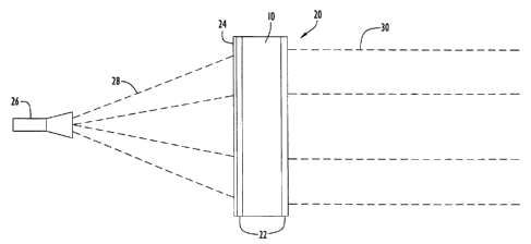
Fig. 1 is a diagrammatic illustration of an RF lens of a present invention
embodiment
21 being illuminated by an RF signal source.
22 Figs. 2A - 2C are views in elevation of exemplary photonic crystal
structures of the type
23 employed by the lens of the present invention embodiments.
24 Fig. 3A is a side view in elevation of an exemplary optical lens.
Fig. 3B is a diagrammatic illustration of a beam being steered by a lower
potion of the
26 lens of Fig. 3A.
27 Fig. 4 is a side view in elevation of a portion of the lens of Fig. 3A.
28 Fig. 5 is a graphical illustration of a far-field intensity pattern
generated by a conventional
29 dish antenna.
2
CA 02622105 2008-02-25
1 Fig. 6 is a graphical illustration of a far-field intensity pattern
generated by the lens of a
2 present invention embodiment.
3 Fig. 7 is a graphical illustration of a cross-sectional profile of the far-
field intensity
4 patterns of Figs. 5 - 6.
Fig. 8 is a graphical illustration of apodization profiles of a beam along
Cartesian (e.g., X
6 and Y) axes of a conventional dish antenna aperture and of a lens of a
present invention
7 embodiment.
8 Fig. 9 is a graphical illustration of the apodization attenuation factor
required to achieve an
9 aperture illumination function.
11 DETAILED DESCRIPTION OF THE PREFERRED EMBODIMENTS
12 The present invention embodiments pertain to a radio frequency (RF) lens
that includes a
13 photonic crystal structure and suppresses side-lobe features. An exemplary
lens according to an
14 embodiment of the present invention being illuminated by an RF signal
source or feed horn is
illustrated in Fig. 1. Specifically, the configuration includes a signal
source 26 and an RF lens 20
16 according to an embodiment of the present invention. Signal source 26 may
be implemented by
17 any conventional or other signal source (e.g., feed horn, antenna, etc.)
and preferably provides an
18 RF signal or beam 28. Lens 20 receives the RF beam from signal source 26
and refracts the beam
19 to produce a collimated RF beam 30. Lens 20 may be utilized for any
suitable RF transmission
and/or reception system.
21 Lens 20 includes a lens portion or layer 10, a plurality of impedance
matching layers 22
22 and an absorption or apodizing layer or mask 24. Lens layer 10 is disposed
between and attached
23 to impedance matching layers 22. Absorption layer 24 is attached to the
impedance matching
24 layer facing signal source 26, where RF beam 28 enters lens 20 and
traverses absorption layer 24,
impedance matching layer 22 and lens layer 10, and exits through the remaining
impedance
26 matching layer as a collimated beam. However, the layers of lens 20 may be
of any quantity,
27 shape or size, may be arranged in any suitable fashion and may be attached
by any conventional
28 or other suitable techniques (e.g., adhesives, etc.).
29 Lens layer 10 includes a photonic crystal structure. An exemplary photonic
crystal
3
CA 02622105 2008-02-25
1 structure for lens layer 10 is illustrated in Fig. 2A. Initially, photonic
crystal structures utilize
2 various materials, where the characteristic dimensions of, and spacing
between, the materials are
3 typically on the order of, or less than, the wavelength of a signal (or
photon) of interest (e.g., for
4 which the material is designed). The materials typically include varying
dielectric constants.
Photonic crystal structures may be engineered to include size, weight and
shape characteristics
6 that are desirable for certain applications. Specifically, lens layer 10 is
formed by defining a
7 series of holes 14 within a parent material 12, preferably by drilling
techniques. However, the
8 holes may alternatively be defined within the parent material via any
conventional techniques or
9 machines (e.g., computer-aided fabrication, two-dimensional machines, water
jet cutting, laser
cutting, etc.). In this case, the two materials that construct the photonic
crystal structure include
11 air (or possibly vacuum for space applications) and parent material 12. The
parent material is
12 preferably an RF laminate and includes a high dielectric constant (e.g., in
the range of 10 - 12).
13 The parent material may alternatively include plastics, a high density
polyethylene, glass or other
14 materials with a low loss tangent at the frequency range of interest and a
suitable dielectric
constant. The hole arrangement may be adjusted to alter the behavior of the
lens layer as
16 described below.
17 Parent material 12 may be of any suitable shape or size. By way of example
only, parent
18 material 12 is substantially cylindrical in the form of a disk and includes
an inner region 16
19 disposed near the disk center and an outer region 18 disposed toward the
disk periphery. Holes 14
are defined within inner and outer regions 16, 18. The holes are generally
defined through the
21 parent material in the direction of (or substantially parallel to) the
propagation path of the beam
22 (e.g., along a propagation axis, or from the lens front surface through the
lens thickness toward
23 the lens rear surface). Holes 14 within outer region 18 include dimensions
less than that of the
24 wavelength of the signal or beam of interest, while the spacing between
those holes are similarly
on the order of or less than the interested signal wavelength. For example, a
hole dimension and
26 spacing each less than one centimeter may be employed for an RF beam with a
frequency of 30
27 gigahertz (GHz). A greater efficiency of the lens may be achieved by
reducing the dimensions
28 and spacing of the holes relative to the wavelength of the signal of
interest as described below.
29 As a photon approaches material 12, an electromagnetic field proximate the
material
4
CA 02622105 2008-02-25
1 essentially experiences an averaging effect from the varying dielectric
constants of the two
2 materials (e.g., material 12 and air) and the resulting dielectric effects
from those materials are
3 proportional to the average of the volumetric capacities of the materials
within the lens layer. In
4 other words, the resulting dielectric effects are comparable to those of a
dielectric with a constant
derived from a weighted average of the material constants, where the material
constants are
6 weighted based on the percentage of the corresponding material volumetric
capacity relative to
7 the volume of the structure. For example, a structure including 60% by
volume of a material with
8 a dielectric constant of 11.0 and 40% by volume of a material with a
dielectric constant 6.0
9 provides properties of a dielectric with a constant of 9.0 (e.g., (60% x
11.0) + (40% x 6.0) = 6.6 +
2.4 = 9.0).
11 Since an optical lens includes greater refractive material near the lens
center portion than
12 that near the lens edge, the photonic crystal structure for lens layer 10
is constructed to similarly
13 include (or emulate) this property. Accordingly, holes 14 defined within
outer region 18 are
14 spaced significantly closer together than holes 14 defined within inner
region 16. The spacing of
holes 14 and their corresponding diameters may be adjusted as a function of
the structure radius to
16 create a lens effect from the entire structure. Thus, the electromagnetic
fields produced by the
17 photonic crystal structure essentially emulate the effects of the optical
lens and enable the entire
18 beam to be steered or refracted. Since the photonic crystal structure is
generally planar or flat, the
19 photonic crystal structure is simple to manufacture and may be realized
through the use of
computer-aided fabrication techniques as described above.
21 The manner in which holes 14 are defined in lens layer 10 is based on the
desired steering
22 or refraction of the RF beam. An exemplary optical lens 25 that steers or
refracts a beam is
23 illustrated in Figs. 3A - 3B and 4. Initially, lens 25 is substantially
circular and includes generally
24 curved or spherical surfaces or faces. The lens may be considered as a
plurality of differential
sections 61 for purposes of describing the steering effect. Each differential
section 61 of lens 25
26 (Fig. 3A) includes a generally trapezoidal cross-section and steers a beam
as if the lens was
27 actually a wedge prism, where an equivalent wedge angle for that section is
a function of the
28 distance of the differential section from the lens center (e.g., the wedge
angle is measured relative
29 to a surface tangent for the lens curved surfaces). In other words, a beam
is refracted according to
5
CA 02622105 2008-02-25
1 a lens local surface gradient in a manner substantially similar to
refraction from a planar surface.
2
3 Specifically, a beam 7 is directed to traverse lens 25. The propagation of
the beam exiting
4 the lens may be determined from Snell's Law as follows.
n, sin 8, = n2 sin eZ (Equation 1)
6 where n, is the index of refraction of the first material traversed by the
beam, n2 is the index of
7 refraction of the second material traversed by the beam, 6/ is the angle of
the beam entering into
8 the second material, and 02 is the angle of the refracted beam within that
material. The
9 steering angles of interest for beam 7 directed toward lens 25 are
determined relative to
propagation axis 60 (e.g., an axis perpendicular to and extending through the
lens front and rear
11 faces) and in accordance with Snell's Law. Thus, each of the equations
based on Snell's Law
12 (e.g., as viewed in Fig. 3B) has the equation angles adjusted by the wedge
angle (e.g., /j as viewed
13 in Fig. 3B) to attain the beam steering value relative to the propagation
axis as described below.
14 Beam 7 enters lens 25 at an angle, e fA, that is within a plane containing
optical axis 80 for
the lens (e.g., the vertical line or axis through the center of the lens from
the thinnest part to the
16 thickest part) and lens propagation axis 60. This angle is the angle of the
beam entry. Since lens
17 25 changes the refraction as a function of the radius from the lens center,
a beam is normal to the
18 particular point upon which the beam impinges. Accordingly, the angle of
beam entry beam, BIA,
19 relative to propagation axis 60 is simply the wedge angle, P, of the lens
(e.g., OIA =/3 as viewed in
Fig. 3B). The beam is refracted at an angle, 02Ai relative to surface norma170
of the lens front
21 surface and determined based on Snell's Law as follows.
22 B2A = sin-' n " sin(BIn) (Equation 2)
n
23 where nQ;, is the index of refraction of air, n is the average index of
refraction of the lens material
24 at the radial location of impact described below and BiA is the angle of
beam entry.
The beam traverses the lens and is directed toward the lens rear surface at an
angle, BIB226 relative to surface norma170 of that rear surface. This angle is
the angle of refraction by the lens
6
CA 02622105 2008-02-25
I front surface, OzAi combined with wedge angles, /j, from the front and rear
lens surfaces and may
2 be expressed as follows.
3 91B = 02A + 2/j (Equation 3)
4 The beam traverses the lens rear surface and is refracted at an angle, 02B,
relative to surface
norma170 of the lens rear surface and determined based on Snell's Law as
follows.
6 92B = sin-' n sin(BiR) (Equation 4)
nair
7 where n is the average index of refraction of the lens material at the
radial location of impact
8 described below, na,r is the index of refraction of air, and BIB is the
angle of beam entry. The
9 angle of refraction, OR, relative to propagation axis 60 is simply the
refracted angle relative to
surface normal 70 of the lens rear surface, 02B, less the wedge angle, /3, of
the lens rear surface
11 (e.g., as viewed in Fig. 3B) and may be expressed as follows.
12 eR = e2a - ~ = sin ' nn sin sin -' I n -'r sin(-/j) I+ 2/.3 -,6 (Equation
5)
urr l M J
13 Referring to Fig. 4, the transverse cross-section of a differential section
61 of exemplary
14 optical lens 25 is symmetric about a plane perpendicular to propagation
axis 60. The lens
typically includes a nominal thickness, tedge, at the lens periphery. The lens
material includes an
16 index of refraction, n j, while the surrounding media (e.g., air) includes
an index of refraction, no,
17 typically approximated to 1.00. An average index of refraction for lens 25
may be determined for
18 a differential section 61 or line (e.g., along the dashed-dotted line as
viewed in Fig. 4) as a
19 function of the distance, r, of that line from the center of lens 25 (e.g.,
as viewed in Fig. 4) as
follows (e.g., a weighted average of index of refraction values for line
segments along the line
21 based on line segment length).
2n, (r- R~ -D2 /4)+2no(C, -(r- R~ -DZ /4))
22 n(r) _ (Equation 6)
Ct - tedge
23 where n, is the index of refraction of lens 25, no is the index of
refraction of air, Rc is the radius
24 of curvature of the lens surface, D is the lens diameter, C, is the center
thickness of the lens, tedge
is the edge thickness of the lens and /j is the wedge angle of section 61. The
edge thickness, tedge,
26 of lens 25 does not contribute to the average index of refraction since the
lens index of refraction
7
CA 02622105 2008-02-25
1 remains relatively constant in the areas encompassed by the edge thickness
(e.g., between the
2 vertical dotted lines as viewed in Fig. 4).
3 The wedge angle,,8, is a function of the distance, r, from the center of the
lens as follows.
4 6(r) = arccos(r / R(. ) (Equation 7)
where Rcis the radius of curvature of the lens surface. Accordingly, the
average index of
6 refraction may be expressed as a function of the wedge angle, /.3, as
follows.
7 2rtt(I~cos(~- FR -DZ l4)+2r,~(C -(I~cos(~- It~ -D'- l4))
(Equation 8)
C, tedge
8 where ni is the index of refraction of lens 25, no is the index of
refraction of air, Rc is the radius
9 of curvature of the lens surface, D is the lens diameter, C, is the lens
center thickness, tedge is the
lens edge thickness and,8 is the wedge angle of section 61. Therefore, a
photonic crystal lens
11 with a particular index of refraction profile provides the same beam
steering characteristics as
12 lens 25 (or sections 61) with wedge angles, P, derived from Equation 8.
13 The average index of refraction for lens 25 is a function of the radius or
distance, r, from
14 the center of the lens. This function is not a constant value, but rather,
follows a function needed
to accomplish the requirements of the lens. The function of an optical lens is
to either focus
16 collimated light into a feed or to re-image the energy from one feed into
another. For the case of
17 focusing collimated light, the bending of the rays follows a simple
formula. A ray hitting the
18 optical lens at a radius or distance, r, from the lens center is deflected
by an angle, 9L, which is a
19 function of the lens Focal length, F!, as follows.
B, = arctan~/F 1 (Equation 9)
21 As described above, Equation 5 provides the angle of the steered or
refracted beam, BR, based on
22 Snell's Law.
23 The properties for lens layer 10 may be obtained iteratively from the above
equations,
24 where the index of refraction for a photonic crystal structure is
equivalent to the square root of the
dielectric constant as described above. In particular, the process commences
with a known or
26 desired optical lens function for emulation by lens 20 (e.g., Equation 9)
and the requirements or
27 properties for the optical lens focal length. A given radial value, r, is
utilized to obtain the
8
CA 02622105 2008-02-25
1 deflection angle, OL, from Equation 9, where the deflection angle is equated
with the refraction
2 angle, 9R, and inserted into Equation 5. Since the average index of
refraction is a function of the
3 wedge angle, #, the wedge angle and/or average index of refraction required
to perform the lens
4 function for the radial value may be determined from Equation 8. This
process is performed
iteratively for radial values, r, to provide an index of refraction profile
for the lens (e.g., the
6 average index of refraction for radial locations on the lens).
7 In order to create photonic crystal lens 20 that emulates the physical
properties of lens 25,
8 holes 14 are arranged within parent material 12 (Fig. 2A) of lens 20 to
create the average index of
9 refraction profile described above. Lens 20 typically includes substantially
planar front and rear
faces normal to the propagation axis (or direction of the beam propagation
path) and emulates the
11 physical properties of the optical lens via produced electromagnetic
fields. However, the index of
12 refraction for a photonic crystal lens is equivalent to the square-root of
the lens dielectric constant
13 (e.g., for materials that exhibit low loss tangents which are preferred for
refracting or steering RF
14 beams). In the case of materials including significant absorption or
scatter, the index of refraction
is a complex value with real and imaginary components. The imaginary component
provides a
16 measure of loss. Since the magnitude of the imaginary component (or loss)
detracts from the real
17 component (or dielectric constant), the dielectric constant differs from
the above relationship in
18 response to significant losses.
19 The effective index of refraction along a portion or line of the photonic
crystal lens is
obtained by taking the average volumetric index of refraction along that line
(e.g., a weighted
21 average of the index of refraction (or dielectric constants of the
materials and holes) along the line
22 based on volume in a manner similar to that described above). The steering
angle, BR, of the
23 resulting photonic crystal lens may be determined based on Snell's Law by
utilizing the effective
24 index of refraction of the photonic crystal lens as the average index of
refraction, n, within
Equation 5 described above. The volumetric average determination should
consider the regions
26 above and below the line (e.g., analogous to distance value, r, described
above). The physical
27 shape of the holes may vary depending on the manufacturing process. One
exemplary
28 manufacturing process includes drilling holes in the prism materials.
9
CA 02622105 2008-02-25
I The orientation of the holes defined in the photonic crystal lens may be
normal to the front
2 and back lens faces (e.g., in a direction of the beam propagation axis or
path). The dimensions of
3 the holes are sufficiently small to enable the electromagnetic fields of
photons (e.g., manipulated
4 by the photonic crystal structure) to be influenced by the average index of
refraction over the lens
volume interacting with or manipulating the photons. Generally, the diameter
of the holes does
6 not exceed (e.g., less than or equal to) one-quarter of the wavelength of
the beam of interest,
7 while the spacing between the holes does not exceed (e.g., less than or
equal to) the wavelength
8 of that beam.
9 Accordingly, an interaction volume for the photonic crystal lens includes
one square wave
(e.g., an area defined by the square of the beam wavelength) as viewed normal
to the propagation
11 axis. Since changes in the photonic crystal structure may create an
impedance mismatch along
12 the propagation axis, the interaction length or thickness of the photonic
crystal lens includes a
13 short dimension. Generally, this dimension of the photonic crystal lens
along the propagation
14 axis (e.g., or thickness) should not exceed 1/16 of the beam wavelength in
order to avoid
impacting the propagation excessively (e.g., by producing back reflections or
etalon resonances).
16 Thus, drilling holes through the thickness of the material is beneficial
since this technique ensures
17 minimal change to the index of refraction along the propagation axis.
18 By way of example, a spacing of holes within the parent material that
provides a minimum
19 average index of refraction (e.g., defined by the largest hole diameter
allowed and determined by
the wavelength of operation as described above) includes the holes spaced
apart from each other
21 in a hexagonal arrangement of equatorial triangles (e.g., each hole at a
corresponding vertex of a
22 triangle) with a minimum wall thickness between holes to provide adequate
mechanical strength.
23 This is a spacing of holes that coincides with the thinnest part of a
conventional lens.
24 Conversely, a spacing of holes within the parent material that may provide
the greatest
average index of refraction is a photonic crystal lens without the presence of
holes. However, the
26 need for a smoothly changing average index of refraction and efficient
control of the direction of
27 the beam energy may put limitations on this configuration. If the photonic
crystal lens is
28 configured to include holes of the same size (e.g., as may be economically
feasible due to
29 manufacturing limitations on machines, such as automated drilling centers),
the maximum
CA 02622105 2008-02-25
1 average index of refraction would be obtained with a minimum of one hole per
interaction
2 volume. This region of the photonic crystal lens corresponds to the thickest
part of lens 25.
3 Referring back to Fig. 1, the use of a parent material with a high
dielectric constant value
4 for lens layer 10 results in a lighter lens, but tends to produce the lens
without the property of
being impedance matched. The lack of impedance matching creates surface
reflections and
6 ultimately requires more power to operate an RF system. Accordingly, lens 20
includes
7 impedance matching layers 22 applied to photonic crystal lens layer 10 to
minimize these
8 reflections. The ideal dielectric constant of impedance matching layers 22
is the square-root of
9 the dielectric constant of lens layer 10. However, due to the variable hole
spacing in the lens layer
(e.g., within inner and outer regions 16, 18) as described above, the
dielectric constant for the lens
11 layer is variable.
12 In order to compensate for the variable dielectric constant of the lens
layer, impedance
13 matching layers 22 similarly include a photonic crystal structure (Fig.
2B). This structure may be
14 constructed in the manner described above for the lens layer and includes a
parent materia132
with an average dielectric constant approximating the square-root of the
average dielectric
16 constant of parent material 12 used for lens layer 10. The parent material
may be of any shape or
17 size and may be of any suitable materials including the desired dielectric
constant properties. By
18 way of example only, parent material 32 is substantially cylindrical in the
form of a disk with
19 substantially planar front and rear surfaces.
Impedance matching layers 22 typically include a hole-spacing pattern similar
to that for
21 lens layer 10, but with minor variations to assure a correct square-root
relationship between the
22 local average dielectric constant of the lens layer and the corresponding
local average dielectric
23 constant of the impedance matching layers. In other words, the hole-spacing
pattern is arranged
24 to provide an average index of refraction (e.g., Equation 6) (or dielectric
constant) profile
equivalent to the square root of the index of refraction (or dielectric
constant) profile of the layer
26 (e.g., lens layer 10) being impedance matched. In particular, the impedance
matching layer
27 thickness is in integer increments of (2n -~)/4 waves or wavelength (e.g.,
1/4 wave, 3/4 wave, 5/4
28 wave, etc.) and is proportional to the square-root of the average index of
refraction of the lens
29 layer being impedance matched as follows.
11
CA 02622105 2008-02-25
1 t n r=(2n -1)A/4 (Equation 10)
2 where t is the impedance layer thickness, X is the wavelength of the beam of
interest, n represents
3 a series instance and n (r) is the average index of refraction of the lens
layer as a function of the
4 distance, r, from the lens center.
Achieving a lower index of refraction with an impedance matching layer may
become
6 infeasible due to the quantity of holes required in the material.
Accordingly, systems requiring
7 impedance matching layers should start with an analysis of the minimum
average index of
8 refraction that is likely to be needed for mechanical integrity, thereby
providing the index of
9 refraction required for the impedance matching layer. The average index of
refraction of the
device to which this impedance matching layer is mated would consequently be
the square of the
11 value achieved for the impedance matching layer.
12 An ideal thickness for the impedance matching layers is one quarter of the
wavelength of
13 the signal of interest divided by the square-root of the (average) index of
refraction of the
14 impedance matching layer (e.g., Equation 10, where the index of refraction
is the square root of
the dielectric constant as described above). Due to the variability of the
dielectric constant (e.g.,
16 as a function of radius) of the impedance matching layer, a secondary
machining operation may
17 be utilized to apply curvature to the impedance matching layers and
maintain one quarter wave
18 thickness from the layer center to the layer edge. The impedance matching
layers may enhance
19 antenna efficiency on the order of 20% (e.g., from 55% to 75%).
A typical illumination pattern on a dish antenna is a truncated exponential
field strength,
21 or a truncated Gaussian. The Gaussian is truncated at the edge of the dish
antenna since the field
22 must get cut-off at some point. At the edge of the dish antenna, the field
strength must go to zero,
23 yet for a typical feed horn arrangement, the field strength at the edge of
the dish antenna is greater
24 than zero. This creates a problem in the far field, where the discontinuous
derivative of the
aperture illumination function creates unnecessarily strong side-lobes. Side-
lobes are the portion
26 of an RF beam that are dictated by diffraction as being necessary to
propagate the beam from the
27 aperture of the antenna. In the far field, the main beam follows a beam
divergence that is on the
28 order of twice the beam wavelength divided by the aperture diameter. The
actual intensity pattern
29 over the entire far field, however, is accurately approximated as the
Fourier transform of the
12
CA 02622105 2008-02-25
I aperture illumination function.
2 Sharp edges in the aperture illumination function or any low order
derivatives creates
3 spatial frequencies in the far field. These spatial frequencies are realized
as lower-power beams
4 emanating from the RF antenna, and are called side-lobes. Side-lobes
contribute to the
detectability of an RF beam, and make the beam easier to jam or eavesdrop. In
order to reduce
6 the occurrence of these types of adverse activities, the side-lobes need to
be reduced. One
7 common technique to reduce side-lobes is to create an aperture illumination
function that is
8 continuous, where all of the function derivatives are also continuous. An
example of such an
9 illumination function is a sine-squared function. The center of the aperture
includes an arbitrary
intensity of unity, while the intensity attenuates following a sine-squared
function of the aperture
11 radius toward the outer aperture edge, where the intensity equals zero.
12 The sine-squared function is a simple function that clearly has continuous
derivatives.
13 However, other functions can be used, and may offer other advantages. In
any event, the
14 illumination function should be chosen to include some level of absorption
of the characteristic
feed horn illumination pattern (e.g., otherwise, gain would be required).
16 Another common technique to reduce the illumination function at the antenna
edge is to
17 configure the edge of a reflective antenna with a series of pointed
triangles (e.g., a serrated edge).
18 This provides a tapered reflection profile and smoothly brings the aperture
illumination function
19 to zero at the edge of the reflector, thereby assisting in the reduction of
side-lobes. However,
these types of structures are not feasible for lenses and may create spatial
frequency effects in the
21 far field due to their physical dimensions typically being greater than the
wavelength of the signal
22 of interest.
23 In order to reduce side-lobes, lens 20 includes apodizing mask 24 that is
truly absorptive
24 for an ideal case. If the attenuation of the illumination pattern occurs
through the use of reflective
techniques (e.g., metal coatings), care must be exercised to control the
direction of those
26 reflections. The apodizing mask is preferably constructed to include a
photonic crystal structure
27 (Fig. 2C) similar to the photonic crystal structures described above for
the lens and impedance
28 matching layers. In particular, holes 14 may be defined within a parent
material 42 with an
29 appropriate absorption coefficient via any suitable techniques (e.g.,
drilling, etc.). The holes are
13
CA 02622105 2008-02-25
1 arranged or defined within the parent material to provide the precise
absorption profile desired.
2 The parent material may be of any shape or size and may be of any suitable
materials including
3 the desired absorbing properties. By way of example only, parent material 42
is substantially
4 cylindrical in the form of a disk with substantially planar front and rear
surfaces.
Material absorption is analyzed to provide the needed absorption profile as a
function of
6 lens radius (as opposed to the index of refraction). Holes 14 are placed in
parent absorber
7 material 42 to create an average absorption over a volume in substantially
the same manner
8 described above for achieving the average index of refraction profile for
the lens layer. The actual
9 function of the apodization profile may be quite complex if a precise beam
shape is required.
However, a simple formula applied at the edge of the aperture is sufficient to
achieve a notable
11 benefit.
12 An example of an apodizing function that may approximate a desired edge
illumination
13 taper for controlling side-lobes is one that includes a 1/r2 function,
where r represents the radius
14 or distance from the lens center. For example, a lens with an incident
aperture illumination
function that is Gaussian in profile and an edge intensity of 20% (of the peak
intensity at the
16 center) may be associated with an edge taper function, yr(r), as follows.
2
17 V(r) = 3(1 r) + 1 (Equation 11)
-
18 The denominator multiplier term (e.g., three) is a consequence of the
illumination function
19 including 20% energy at the edge of the aperture. This multiplier may vary
according to the
energy value at the edge of the aperture. Equation 11 provides the absorption
ratio as a function
21 of radius, which can be summarized as the ratio of the absorbed energy over
the transmitted
22 energy. The value for the radius is normalized (e.g., radius of r,,," = 1)
for simplicity. This
23 function closely approximates the ideal apodization function. However,
minor variations to the
24 function may be desired for an optimized system.
In order to realize this function within photonic crystal apodizing mask 24, a
series of
26 holes 14 are placed within parent material 42 that is highly absorptive to
radio waves (e.g., carbon
27 loaded material, etc.). The average absorption of the material (e.g., a
weighted average of the
28 absorption of the material and holes (e.g., the holes should have no
absorption) based on volume
14
CA 02622105 2008-02-25
1 and determined in a manner similar to the weighted average for the
dielectric constant described
2 above) over the interaction volume of the lens provides the value of the
absorption for the
3 apodizing mask. The mask absorption divided by the unapodized case should
yield an
4 approximate value resulting from Equation 11. Thus, holes 14 are placed in
parent materia142 in
a manner to provide the absorption values to produce the desired absorption
profile. Apodizing
6 mask 24 may be configured with holes 14 closely spaced together (Fig. 2C)
when this layer is
7 mounted to other layers of the lens. In this case, the mechanical integrity
for the apodizing mask
8 is provided by the layers to which the apodizing mask is mounted, thereby
enabling the closely
9 spaced arrangement of holes 14.
The apodizing mask is simple to manufacture through the use of computer-aided
11 fabrication techniques as described above. Equation 11 may be modified to
accommodate feeds
12 that do not produce energy distributions with a Gaussian profile and
achieve the desired results.
13 Figs. 5 - 6 illustrate an exemplary far-field intensity pattern of an
unapodized aperture and
14 an apodized aperture of lens 20, respectively. The intensity magnitudes
within the pattern are
indicated by the shading illustrated in the key (e.g., as viewed in Figs. 5 -
6). The unapodized
16 case (Fig. 5) is for a conventional dish antenna illuminated by a feed horn
and with a 20%
17 illumination cut-off at the edge. The feed horn is prime-mounted and
supported by a three-vane
18 spider support. The apodized case (Fig. 6) shows the far-field pattern for
lens 20 (e.g., an
19 unobstructed aperture photonic crystal lens manufactured to deliver
diffraction-limited beam
divergence). Fig. 7 illustrates the cross-section far field intensity pattern
for the unapodized and
21 apodized cases. The intensity patterns are graphically plotted along X and
Y axes respectively
22 representing the field angle and normalized intensity (as viewed in Fig.
7). The apodized case has
23 a slightly larger main-beam divergence, but greatly suppressed side-lobes,
especially far from the
24 main beam. Side-lobe suppression reaches factors of approximately 1,000
where the side-lobe
energy is strongest.
26 Fig. 8 illustrates apodization or absorption profiles of the RF beam along
Cartesian (e.g.,
27 X and Y) axes of a conventional dish antenna aperture and of the aperture
of lens 20. The
28 illumination patterns are graphically plotted along X and Y axes
respectively representing the
29 pupil coordinates (e.g., radial normalized coordinates) and normalized
intensity (e.g., as viewed in
CA 02622105 2008-02-25
1 Fig. 8). The conventional dish antenna absorption or illumination pattem is
truncated, while lens
2 20 provides the sine-squared absorption function or illumination pattern
described above. Fig. 9
3 illustrates the apodization attenuation factor required to attain the
aperture illumination function,
4 assuming a Gaussian beam profile truncated at approximately 20% at the
aperture edge (e.g., as
shown in Fig. 8 for the conventional dish antenna). The attenuation profile is
graphically plotted
6 along X and Y axes respectively representing the pupil coordinates (e.g.,
normalized based on the
7 radius) and attenuation factor (e.g., as viewed in Fig. 9).
8 Lens 20 may be utilized to create virtually any type of desired beam
steering or pattern.
9 Thus, several lenses may be produced each with a different hole pattern to
provide a series of
interchangeable lenses for an RF system (Fig. 1). In this case, a photonic
crystal lens may easily
11 be replaced within an RF system with other lenses including different hole
patterns to attain
12 desired (and different) beam patterns. Further, the photonic crystal
structure may be configured to
13 create any types of devices (e.g., quasi-optical, lenses, prisms, beam
splitters, filters, polarizers,
14 etc.) in substantially the same manner described above by simply adjusting
the hole dimensions,
geometries and/or arrangements within a parent dielectric material to attain
the desired beam
16 steering and/or beam forming characteristics.
17 It will be appreciated that the embodiments described above and illustrated
in the
18 drawings represent only a few of the many ways of implementing a radio
frequency lens and
19 method of suppressing side-lobes.
The lens may include any quantity of layers arranged in any suitable fashion.
The layers
21 may be of any shape, size or thickness and may include any suitable
materials. The lens may be
22 utilized for signals in any desired frequency range. The lens layer may be
of any quantity, size or
23 shape, and may be constructed of any suitable materials. Any suitable
materials of any quantity
24 may be utilized to provide the varying dielectric constants (e.g., a
plurality of solid materials,
solid materials in combination with air or other fluid, etc.). The lens layer
may be utilized with
26 or without an impedance matching layer and/or apodizing mask. The lens
layer parent and/or
27 other materials may be of any quantity, size, shape or thickness, may be
any suitable materials
28 (e.g., plastics, a high density polyethylene, RF laminate, glass, etc.) and
may include any suitable
29 dielectric constant for an application. The parent material preferably
includes a low loss tangent
16
CA 02622105 2008-02-25
1 at the frequency range of interest. The lens layer may be configured (or
include several layers that
2 are configured) to provide any desired steering effect or angle of
refraction or to emulate any
3 properties of a corresponding material or optical lens. The lens layer may
further be configured to
4 include any combination of beam forming (e.g., lens) and/or beam steering
(e.g., prism)
characteristics.
6 The holes for the lens layer may be of any quantity, size or shape, and may
be defined in
7 the parent and/or other material in any arrangement, orientation or location
to provide the desired
8 characteristics (e.g., beam steering effect, index of refraction, dielectric
constant, etc.). The
9 various regions of the lens layer parent material may include any desired
hole arrangement and
may be defined at any suitable locations on that material to provide the
desired characteristics.
11 The holes may be defined within the parent and/or other material via any
conventional or other
12 manufacturing techniques or machines (e.g., computer-aided fabrication
techniques,
13 stereolithography, two-dimensional machines, waterjet cutting, laser
cutting, etc.). Alternatively,
14 the lens layer may include or utilize other solid materials or fluids to
provide the varying
dielectric constants.
16 The impedance matching layer may be of any quantity, size or shape, and may
be
17 constructed of any suitable materials. Any suitable materials of any
quantity may be utilized to
18 provide the varying dielectric constants (e.g., a plurality of solid
materials, solid materials in
19 combination with air or other fluid, etc.). The parent and/or other
materials of the impedance
matching layer may be of any quantity, size, shape or thickness, may be any
suitable materials
21 (e.g., plastics, a high density polyethylene, RF laminate, glass, etc.) and
may include any suitable
22 dielectric constant for an application. The parent material preferably
includes a low loss tangent
23 at the frequency range of interest. The impedance matching layer may be
configured (or include
24 several layers that are configured) to provide impedance matching for any
desired layer of the
lens.
26 The holes for the impedance matching layer may be of any quantity, size or
shape, and
27 may be defined in the parent and/or other material in any arrangement,
orientation or location to
28 provide the desired characteristics (e.g., impedance matching, index of
refraction, dielectric
29 constant, etc.). The holes may be defined within the parent and/or other
material via any
17
CA 02622105 2008-02-25
1 conventional or other manufacturing techniques or machines (e.g., computer-
aided fabrication
2 techniques, stereolithography, two-dimensional machines, water jet cutting,
laser cutting, etc.).
3 Alternatively, the impedance matching layer may include or utilize other
solid materials or fluids
4 to provide the varying dielectric constants.
The apodizing mask may be of any quantity, size or shape, and may be
constructed of any
6 suitable materials. Any suitable materials of any quantity may be utilized
to provide the desired
7 absorption coefficient or absorption profile (e.g., a plurality of solid
materials, solid materials in
8 combination with air or other fluid, etc.). The parent and/or other material
of the apodizing
9 mask mav be of any quantity, size, shape or thickness, may be any suitable
materials (e.g.,
plastics, a high density polyethylene, RF laminate, carbon loaded material,
etc.) and may include
11 any suitable radio or other wave absorption characteristics for an
application. The parent material
12 is preferably implemented by a material highly absorptive to radio waves.
The apodizing mask
13 may be configured (or include several layers that are configured) to
provide the desired absorption
14 profile.
The holes for the apodizing mask may be of any quantity, size or shape, and
may be
16 defined in the parent and/or other material in any arrangement, orientation
or location to provide
17 the desired characteristics (e.g., side-lobe suppression, absorption,
etc.). The holes may be
18 defined within the parent and/or other material via any conventional or
other manufacturing
19 techniques or machines (e.g., computer-aided fabrication techniques,
stereolithography, two-
dimensional machines, water jet cutting, laser cutting, etc.). Alternatively,
the apodizing mask
21 may include or utilize other solid materials or fluids to provide the
absorption properties. The
22 apodizing mask may be configured to provide the desired absorbing
properties for any suitable
23 taper functions.
24 The layers of the lens (e.g., lens layer, impedance matching, apodizing
mask, etc.) may be
attached in any fashion via any conventional or other techniques (e.g.,
adhesives, etc.). The lens
26 may be utilized in combination with any suitable signal source (e.g., feed
horn, antenna, etc.), or
27 signal receiver to steer incoming signals. The lens may be utilized to
create virtually any type of
28 desired beam pattern, where several lenses may be produced each with a
different hole pattern to
29 provide a series of interchangeable lenses to provide various beams for RF
or other systems.
18
CA 02622105 2008-02-25
1 Further, the photonic crystal structure of the lens may be utilized to
create any beam
2 manipulating device (e.g., prism, beam splitters, filters, polarizers, etc.)
by simply adjusting the
3 hole dimensions, geometries and/or arrangement within the parent and/or
other materials to attain
4 the desired beam steering and/or beam forming characteristics.
It is to be understood that the terms "top", "bottom", "front", "rear",
"side", "height",
6 "length", "width", "upper", "lower", "thickness", "vertical", "horizontal"
and the like are used
7 herein merely to describe points of reference and do not limit the present
invention embodiments
8 to any particular orientation or configuration.
9 From the foregoing description, it will be appreciated that the invention
makes available a
novel radio frequency lens and method of suppressing side-lobes, wherein a
radio frequency (RF)
11 lens includes a photonic crystal structure and suppresses side-lobe
features.
12 Having described preferred embodiments of a new and improved radio
frequency lens and
13 method of suppressing side-lobes, it is believed that other modifications,
variations and changes
14 will be suggested to those skilled in the art in view of the teachings set
forth herein. It is therefore
to be understood that all such variations, modifications and changes are
believed to fall within the
16 scope of the present invention as defined by the appended claims.
19