Note: Descriptions are shown in the official language in which they were submitted.
CA 02622272 2008-02-26
OPTICAL WAVEGUIDE DEVICE AND
MANUFACTURING METHOD FOR OPTICAL WAVEGUIDE DEVICE
CROSS-REFERENCE TO RELATED APPLICATION
This application is based upon and claims the benefit
of priority from Japanese patent application No. 2007-077566,
filed on March 23, 2007, the disclosure of which is
incorporated herein in its entirety by reference.
BACKGROUND OF THE INVENTION
1. Field of the Invention
The present invention relates to an optical waveguide
device and the like, in particular, to an optical waveguide
device and a manufacturing method for an optical waveguide
device with which accuracy and productivity improves when an
optical device is mounted on a corresponding position of an
optical waveguide.
2. Description of the Related Art
An optical transceiver used in an optical access market
includes a module in a micro-optics type composed of an LD, a
PD, a thin film filter, a lens, and the like, and a PLC
module composed of a silica waveguide formed on a silicon
substrate which is further mounted with an LD and a PD by
hybrid mounting. The both have advantages and disadvantages.
However, the latter is more advantageous in terms of a cost
CA 02622272 2008-02-26
2
and delivery because it is less complicated than the former
that needs to align optical axes of each component with
monitoring an optical output. The latter utilizes a
technique generally called passive alignment for the hybrid
mounting.
In the passive alignment, a positional accuracy of a
mounting component in a planar direction with respect to an
optical waveguide section is secured by recognizing an image
of an alignment marker formed on the mounting component. In
addition, a positional accuracy in a vertical direction is
secured according to a platform formed on the substrate.
Since the height of this platform can be formed with high
accuracy, a height thereof can be aligned with a height of
the optical waveguide with high accuracy by only mounting the
optical device on the platform.
Figs. 12 and 13 show examples of an optical waveguide
device constructed with the passive alignment. In the
example shown in Fig. 12, an optical waveguide device 50
formed in a planar shape includes an optical waveguide
forming section 56 formed on a substrate 51 made of silicon
crystal, and an optical device mounting section 57 provided
in response to the above. The optical waveguide forming
section 56 is composed of an optical waveguide section 55
including a base layer 521, a lower cladding layer 522, an
optical waveguide core 53, and an upper cladding layer 54,
formed on the silicon substrate 51.
CA 02622272 2008-02-26
3
In addition, the optical device mounting section 57 is
composed of an optical device 58 mounted so as to be coupled
optically with an end face (a left end face in Fig. 13) of
the optical waveguide core 53 which is exposed because the
optical waveguide forming layer 55 is partially removed, and
four platform blocks 59 for setting the height of the optical
device 58 with high accuracy. Top end faces of each platform
block 59 include chromium films 61. A semiconductor laser
chip (LD) is used as the optical device 58. The optical
device 58 is fixed on the platform blocks 59 in a condition
where optical axes of an active layer 58A in the optical
device 58 and the optical waveguide core 53 in the optical
waveguide section 55 are aligned.
The optical device mounting section 57 includes the
aforementioned platform blocks 59 formed with a same film as
the base layer 521, and marker tables 60 provided with
alignment markers (made of a chromium film, two of them are
formed in right and left sides) on the top end face for
adjusting a position. The platform blocks 59 are patterned
from the same film with the base layer 521, so that the
platform blocks 59 and the base layer 521 are in the same
height. When the optical device 58 is mounted, the optical
device 58 is supported on the platform blocks 59. The base
layer 521, the lower cladding layer 522, the optical
waveguide core 53, and the upper cladding layer 54 are formed
with a CVD respectively.
CA 02622272 2008-02-26
4
Meanwhile, an alignment of the optical device 58 in the
planar direction is performed by using two of the substrate
side alignment markers 62 provided in the right and left
sides in the optical device mounting area 57. The alignment
marker tables 60 holding the substrate side alignment markers
62 is in a cylindrical shape, and fix the substrate side
alignment markers 62 made of a metal film (a chromium film)
thereon. A center position of the circle on the top surface
of the substrate side alignment marker 62 is adjusted with
high accuracy based on a position of the waveguide core 53 in
the optical waveguide section 55.
As shown in Fig. 13, there are two of optical device
side alignment markers 58a provided in a bottom surface of
the optical device 58, corresponding to the substrate side
alignment markers 62. The optical device side alignment
markers 58a are, as shown in Fig. 14, formed as a metal film
pattern in a circular punched shape, and the centers of the
circles are arranged in the right and left sides and aligned
with high accuracy based on a position of the active layer
58A in the optical device 58. Further, positions of the
optical device side alignment markers 58a and the substrate
side alignment markers 62 are specified so that the optical
device 58 is placed in a right position to be fixed when the
centers of those optical device side alignment markers 58a
and the substrate side alignment markers 62 are matched with
each other.
CA 02622272 2008-02-26
When the optical device 58 is actually mounted as shown
in Figs. 12 and 13, the metal film patterns in the optical
device 58 side (the optical device side alignment markers
58a) and the substrate side alignment markers 62 are
5 superimposed by the image recognition as shown in Fig. 14.
In this case, infrared light is emitted from the substrate 51
side, as shown in Fig. 13, and a monitoring camera 52
disposed upward monitors transmitted light. Consequently,
images as shown in Fig. 14 can be obtained because the metal
part shields the infrared light.
The diagram in the left side in Fig. 14 shows a case in
which the center axes of the substrate side alignment markers
62 and the LD side alignment markers 58a are not aligned with
each other on the substrate 51 when the optical device 58 is
going to be mounted. Further, the diagram in the right side
in the same figure shows a case in which the center axes of
the substrate side alignment markers 62 and the LD side
alignment markers 58a are aligned.
Each position of the substrate side and the optical
device side alignment markers 62, 58a are specified with high
accuracy with respect to the positions of the waveguide core
53 in the optical waveguide section 56 and the active layer
58A of the optical device, respectively. Therefore, if the
optical device is mounted on a position where the center of
the circles for both are aligned, optical axes of the active
layer 58A and the optical waveguide core 53 in the planar
CA 02622272 2008-02-26
6
direction can be aligned with high accuracy.
As for the optical waveguide device of this type, a
technique disclosed by Japanese Patent Application Laid-open
No. 2002-062447 (Patent Document 1) has been known. In the
technique, as alignment markers, short linear markers
parallel to the optical axis are formed at the position where
each end face of the optical waveguide section and the
optical device section are abutted, and alignment is
performed at the position the markers are abutted and matched.
According to the technique, the optical waveguide section and
the optical device section can be aligned while both are
abutted. Therefore, the alignment can be performed by the
adjustment in a direction along with the end faces of those
only, and two-dimensional alignment is not required.
As shown Figs. 12 and 13 with respect to the
aforementioned related art, in order to make it possible to
align each optical axis of the optical waveguide core 53 and
the active layer 58A in the optical device side according to
the alignment of the center axes of the optical waveguide
side alignment markers 62 and the optical device side
alignment markers 58a, it is required that the centers of
each marker corresponding to the waveguide core 53 side (or
the active layer 58A side in the optical device 58) are
specified with high accuracy in advance.
Meanwhile, when the optical waveguide device is mass-
produced, a number of optical waveguide chips are produced on
CA 02622272 2008-02-26
7
a silicon wafer at the same time. The silicon wafer
processing includes a lot of processes in which the whole
wafer is stressed with a thermal process, a film formation,
and the like. Therefore, when the substrate side alignment
markers 62 provided in the optical device mounting area 57
and the optical waveguide core 53 provided in the optical
waveguide section 55 are patterned respectively, the accuracy
of position adjustment for both are different in some cases
due to variations of distortion degree in the wafer. Further,
the optical waveguide core 53 and the corresponding substrate
side alignment markers 62 are formed in different layers, and
their position adjustments are performed in different
processes respectively. Therefore, their relative positions
are depending on the accuracy of each position adjustment,
and the positions thereof are not always stabilized. An
example of this case is shown in Fig. 15.
In Fig. 15, the optical waveguide core 53 and the
substrate side alignment markers 62 are provided on the same
substrate 51. Further, both of the active layer 58A and the
optical device side alignment markers 58a are provided in the
optical device section 58 (refer to Figs. 12 and 13). X
marks in Fig. 15 express, in the optical device mounting area
57, proper positions in which the substrate side alignment
markers 62 are supposed to exist (theoretically). On the
other hand, actual positions of the substrate side alignment
markers 62 are recognized by the monitoring camera and the
CA 02622272 2008-02-26
8
like, which are shifted in some cases from the points
expressed by X marks.
This is because the accuracy in the position adjustment
varies due to the distortion of the wafer caused by the
stress when each section in a module is patterned. Therefore,
when the optical device 58 is mounted after the centers of
the substrate side alignment markers 62 are aligned with the
centers of the optical device side alignment markers 58a
according to the method in the case of Fig. 14, a problem can
occur where the optical axes of the waveguide core 53 and the
active layer 58A are not aligned with each other as shown in
Fig. 15. However, in the aforementioned example, there is no
way to detect proper positions in which the substrate side
alignment markers are supposed to exist. Therefore, it is
impossible to know how much the misalignment amount is, and,
in addition, it is impossible even to judge whether there is
the misalignment or not. Accordingly, an output rate of non-
defective products is declined because of the trouble
accompanied by the optical device mounting.
The technique disclosed in Patent Document 1 is
suitable for the position adjustment only in a direction
along with the end faces where the optical waveguide section
and the optical device section are matched. However, various
transformations practically occurs in the substrate, the
device section, and the like, which are caused by distortion
due to a problem of processing accuracy or stress.
CA 02622272 2008-02-26
9
Accordingly, the two-dimensional position adjustment
including angular adjustment is required when the optical
device section is to be mounted. It is very difficult for a
one-dimensional linear alignment marker to perform this
adjustment. For example, a big problem occurs if an optical
axis of an optical waveguide is misaligned even by 1 - 2
degrees, however, such a small misalignment cannot be
recognized practically with an alignment marker having a
length far shorter than the optical waveguide. Further, the
length of the alignment marker cannot be extended because an
image needs to be within a screen of a monitor for the
alignment. Therefore, this technique is not efficient in any
alignment other than the one-dimensional alignment.
SUMARRY OF THE INVENTION
An exemplary object of the present invention is to
provide an optical waveguide device, and a manufacturing
method therefor which suppress effectively a harmful
influence such as variations of patterning accuracy for an
alignment marker due to distortion caused by stress on a
substrate including an optical waveguide, with which mounting
accuracy and productivity can be improved.
In order to achieve the exemplary object, the optical
waveguide device according to an exemplary aspect of the
present invention is one in which an optical device is
aligned by an alignment marker so as to be mounted by hybrid
CA 02622272 2008-02-26
mounting on a substrate on which an optical waveguide core is
formed, wherein a fiducial marker for adjusting a mounting
position of the optical device is provided at an absolute
position on a basis of the optical waveguide core so that the
5 optical waveguide core and the optical device are optically
coupled.
The manufacturing method for an optical waveguide
device according to anther exemplary aspect of the present
invention is a method with which an optical device is aligned
10 by an alignment marker so as to be mounted by hybrid mounting
on a substrate on which an optical waveguide core is formed,
wherein a fiducial marker for adjusting a mounting position
of the optical device is formed at an absolute position on a
basis of the optical waveguide core so that the optical
waveguide core and the optical device is optically coupled.
As an exemplary advantage according to the invention, a
regular mounting position of the optical device can be
specified constantly depending on especially the fiducial
marker provided in the optical waveguide side on the
substrate. Therefore, if distortion occurs in an optical
device mounting area, an amount of misalignment can be
corrected with respect to the mounting position of the
optical device. Accordingly, the optical device can be
surely arranged at the regular position when the optical
device is mounted, and it is possible to provide an excellent
and unprecedented optical waveguide device and the
CA 02622272 2008-02-26
11
manufacturing method for an optical waveguide device with
which mounting accuracy and productivity can improve.
BRIEF DESCRIPTION OF THE DRAWINGS
Fig. 1 is an exploded perspective view showing one
exemplary embodiment of an optical waveguide device according
to the invention;
Fig. 2A is a plan view showing an optical device, which
is a mounting target, in the optical waveguide device in Fig.
1, and Fig. 2B is a plan view showing a substrate part
including a waveguide core in a main body side of the optical
waveguide device in Fig. 1;
Fig. 3 is an explanatory diagram showing each specific
example of fiducial marker shapes disclosed in Fig. 1;
Fig. 4 is an explanatory diagram showing procedures 4A
to 4L for mounting the fiducial marker disclosed in Fig. 1 on
the substrate;
Fig. 5 is a general configuration diagram showing an
overall optical device mounting system in a case where the
optical device disclosed in Fig. 1 is mounted;
Fig. 6 is a block diagram showing one example of a main
controller disclosed in Fig. 5;
Fig. 7 is a flowchart showing operations of the optical
device mounting system disclosed in Fig. 5;
Fig. 8 is an explanatory diagram showing a positional
relationship between the fiducial markers and the substrate
CA 02622272 2008-02-26
12
side alignment markers provided on the substrate in Fig. 1,
and a misalignment state of the substrate side alignment
markers in conjunction with distortion of the substrate;
Fig. 9 is an explanatory diagram showing a case where,
on the substrate with which the misalignment has occurred in
Fig. 8, centers of the substrate side alignment markers are
matched with centers of the LD alignment markers in the
optical device side (the optical device is in a mounted
condition);
Fig. 10 is an explanatory diagram showing a positional
relationship between each marker in a case where a mounting
position for the optical device is finely adjusted from the
mounted condition of the optical device shown in Fig. 9 so
that a center axis of an LD active layer is aligned with a
center axis of the waveguide core;
Fig. 11 is an explanatory diagram showing a case where
the center axis of the LD active layer is aligned with the
center axis of the waveguide core by performing the mounting
operation in Fig. 10;
Fig. 12 is an exploded perspective view showing an
optical waveguide device of a related art;
Fig. 13 is an explanatory diagram showing a mounted
condition of an optical device which is a result of
performance shown in Fig. 12;
Fig. 14 is an explanatory diagram showing a positional
relationship between markers in a case where the optical
CA 02622272 2008-02-26
13
device is mounted with shifted from a regular mounting
position in the optical device mounting of Fig. 12, and where
the mounted position is finely adjusted from the misaligned
mounting position so that the optical device is transferred
to a regular position (where an center axis of an optical
waveguide core is matched with an center axis of an LD active
layer) ; and
Fig. 15 is an explanatory diagram showing a
misalignment condition of the optical device in Fig. 14.
DESCRIPTION OF EXEMPLARY EMBODIMENTS
Hereinafter, one exemplary embodiment of the invention
will be explained with reference to the accompanying drawings.
Fig. 1 shows a conceptually exploded perspective view of the
optical waveguide device according to the exemplary
embodiment. Figs. 2A and 2B show plan views of the same. In
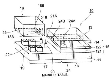
Fig. 1, an optical waveguide device 10 includes a substrate
11 made of a silicon crystal, an optical waveguide forming
section 16 provided on a portion of the substrate 11, an
optical device mounting section 17 (an optical device
mounting area) provided on another portion of the substrate
11, corresponding to the optical waveguide forming section 16.
The optical waveguide forming section 16 includes an optical
waveguide section 15 formed with a base layer 121, a lower
cladding layer 122, an optical waveguide core 13, and an
upper cladding layer 14 laminated on the substrate 11, all of
CA 02622272 2008-02-26
14
which is made of a CVD film.
With respect to forming the optical waveguide section
15 and the optical device mounting section 17, each layer is
firstly formed to be a film and processed all over a surface
of the substrate 11, and then platform blocks 19 and marker
tables 20 are formed in an area of the optical device
mounting section 17 by etching. The platform blocks 19 and
the marker tables 20 are formed by the same film with the
base layer 121, and previously patterned chromium layers 21A,
21B, and 22 on the film are used as a mask when they are
etched. Accordingly, such a structure can be realized. On
the other hand, the optical waveguide core 13 and the
fiducial marker tables 24 are formed by the same film, and
both are aligned and formed together by a same mask to be
patterned. Then, the fiducial marker tables 24 are formed at
absolute positions based on the waveguide core 13. A
chromium film is formed on the top surface of the fiducial
markers 24. Accordingly, fiducial markers 24A and 24B are
composed of the fiducial marker tables 24 and the chromium
films.
As described above, the fiducial markers 24A, 24B are
formed at the absolute position based on the optical
waveguide core 13. Therefore, it becomes an absolute
fiducial point when the optical device 18 is aligned so that
the optical waveguide core 13 and the optical device 18 are
optically coupled.
CA 02622272 2008-02-26
The optical device 18 is mounted on the optical device
mounting section 17 so as to be coupled optically with an end
face of the optical waveguide core 13 which is exposed on a
cross-section of the optical waveguide section 15.
5 Accordingly, the optical waveguide device 10 is formed. In
this exemplary embodiment, a semiconductor laser chip is used
in the optical device 18. Hereinafter, the whole optical
device including the semiconductor laser chip is described as
an LD.
10 Namely, in the exemplary embodiment of Fig. 1, the
optical waveguide device 10 includes the optical waveguide
section 15 including the optical waveguide core 13 formed on
the substrate 11, and the optical device 18 (the LD) in an
end face light emitting type fixed on the substrate 11 so as
15 to correspond to the optical waveguide section 15. The
optical waveguide section and the optical device are mounted
by hybrid mounting on the substrate 11 so that both light end
faces are coupled with each other. Thus, the optical
waveguide device 10 is formed.
The LD side alignment markers 18A and 18B are provided
on the bottom surface of the optical device 18, at the both
sides of an LD active layer 25. Further, substrate side
alignment markers 21A and 21B are provided on the substrate
11 on which the optical device 18 is to be mounted. The
substrate side alignment markers 21A and 21B are arranged in
positions where centers thereof are matched with centers of
CA 02622272 2008-02-26
16
the LD side alignment markers 18A and 18B which are on the
optical device 18 side, when the optical device 18 is mounted.
As described in the aforementioned example, in the
manufacturing processing of the optical waveguide device 10,
the alignment accuracy is sometimes varied when the substrate
side alignment markers 21A and 21B is patterned because a
silicon wafer which is a material of the substrate 11 is
sometimes distorted due to the thermal process or the like.
In such a case, even if the LD side alignment markers 18A and
18B of the optical device 18 are placed to be corresponded to
the substrate side alignment markers when the optical device
18 is mounted, the positions of the LD active layer 25 in the
optical device 18 side and the waveguide core 13 in the
optical waveguide section 15 side are not matched completely
with each other (refer to Fig. 15) in some cases.
With the above situation, in this exemplary embodiment,
two markers which can be used as absolute fiducial are
provided so as to determine a misalignment direction and a
misalignment amount between proper positions and actual
positions of the substrate side alignment markers. These
fiducial markers 24A and 24B are formed near the optical
waveguide core 13 at the same time when the optical waveguide
core 13 is patterned on the substrate 11, as described.
Accordingly, relative positions of the optical waveguide core
13 and the fiducial markers 24A and 24B are kept to be
constantly stable, and, unlike a case with the substrate side
CA 02622272 2008-02-26
17
alignment markers 21A and 21B, misalignment with respect to
the optical waveguide core 13 is not occurred during the
manufacturing process.
Because such fiducial markers 24A and 24B are provided,
the proper positions (the regular positions) for the
substrate side alignment markers 21A and 21B with respect to
the fiducial markers 24A and 24B can be recognized. If the
optical device mounting position is determined taking a
difference between the regular positions and the actual
positions of the alignment markers as a correction value, the
optical waveguide core 13 in the optical waveguide section 15
and the active layer 25 in the optical device 18 side can be
matched with each other aligning those center axes
immediately and with high accuracy, which will be described
later.
The aforementioned fiducial markers and other markers
will be explained. The number of the fiducial marker to be
provided may be one, but there are two of those fiducial
markers (24A, 24B) provided in the forming area of the
optical waveguide section 15 in this exemplary embodiment.
That is, the fiducial markers 24A and 24B are provided in
both sides of the optical waveguide core 13 in the optical
waveguide section 15 on the substrate 11, as shown in Figs. 1
and 2. Each fiducial marker 24A and 24B are constructed
comparably solidly by the chromium film. Further, an area
formed by connecting those two of the fiducial markers 24A,
CA 02622272 2008-02-26
18
24B and aforementioned two of the substrate side alignment
markers 21A and 21B is designed in a rectangle having each
internal angle of 90 degrees in the exemplary embodiment,
which leads to an immediate calculation of the misalignment
amount and an immediate mounting operation, described later.
In this regard, the area surrounded by the segments
connecting each of the fiducial markers 24A, 24B and the
substrate side alignment marker 21A, 21B is not limited in
the shape mentioned above in the exemplary embodiment of the
invention. The shape may be another specified square shape
having internal angle of degrees other than 90 degrees.
Further, in this exemplary embodiment, two of the fiducial
markers are provided at the absolute positions based on the
optical waveguide core, but the number of the fiducial
markers is not limited by the above. The number may be
selected accordingly as long as one or more of the fiducial
markers is provided.
These fiducial markers 24A, 24B, and the above
mentioned optical waveguide core 13 are formed together from
a film in the same layer by photolithography using the same
mask, so that a positional relationship between them does not
vary depending on a problem such as a matching accuracy.
The substrate side alignment markers 21A, 21B, and the
fiducial markers 24A, 24B are formed as light shielding films
each of which are in almost same shapes with upper surfaces
of the marker tables 20 and the fiducial marker tables 24.
CA 02622272 2008-02-26
19
These light shielding films are used for marker recognition
with transmitted infrared light. However, even if the light
shielding films are not included, the marker can be
recognized by using diffraction at a lateral part of the
marker table, incident light, or the like. Further,
corresponding to two of the substrate side alignment markers
21A, 21B, two of the LD side alignment markers 18A and 18B in
an opening type provided in a bottom surface side of the
optical device 18 are formed with a light shielding film in a
square shape inside of which is opened in a circular shape.
This light shielding film is formed by a gold film.
In this case, the above mentioned opening type LD side
alignment markers 18A and 18B may be replaced by a light
reflective film having a simple geometric patterned inner
side opening, with which a center position can be specified
easily, with a polygonal shaped outer side, instead of the
reflective film having the circular shaped inner side opening
with a square shaped outer side. Fig. 3 shows various
examples of the fiducial markers 24A, 24B and the alignment
markers 21A, 21B, 18A, 18B. Fig. 3A shows shapes of
reflective surfaces, inside of the shapes are reflective
surfaces. Fig. 3B shows various examples of punched shapes
which have square shaped outer sides and geometric shaped
inner sides.
In the example of Fig. 3, it is not limited which
markers are to be used as the fiducial markers 24A, 24B and
CA 02622272 2008-02-26
which markers are to be used as the alignment markers 21A,
21B, 18A, 18B. Anything can be selected freely to be used
therefor. Although markers are not limited in those shapes
particularly, the one disclosed in Figs. 1 and 2 is selected
5 to be used in the above exemplary embodiment.
Next, a manufacturing method will be explained
hereinafter with reference to Fig. 4, in which the fiducial
markers 24A, 24B and the substrate side alignment markers 21A,
21B are arranged at the positions disclosed in Fig. 1 on the
10 substrate 11.
Firstly, a silicon oxide film, which is to be a first
layer of a base layer 121, is formed on the silicon substrate
11 (Fig. 4A), and then chromium films 21 and 22 are patterned
at each predetermined position in a predetermined shape on
15 the base layer 121 so as to be used as the masks when the
platform blocks 19 and the marker tables 20 of the substrate
side alignment markers are formed later (Fig. 4B). Next, a
silicone oxide film which is to be a second layer of the
lower cladding layer 122 is formed (Fig. 4C). A silicone
20 oxide film 13d having high refraction index, which is to be
the optical waveguide core 13, is laminated thereon (Fig. 4D).
A chromium film 13e is further formed on the silicon
oxide film 13d and resist 13f is applied thereon (Fig. 4E).
The optical waveguide core 13 and the fiducial markers 24A,
24B are patterned together by the photolithography, and the
silicon oxide film 13d and the chromium film 13e are etched
CA 02622272 2008-02-26
21
by reactive ion etching, and then the optical waveguide core
13 and the fiducial marker tables 24 are formed (Fig. 4F).
The chromium films on upper surfaces of the fiducial marker
tables 24 in this case are to be the fiducial markers 24A and
24B.
Next, the resist 13f is removed once, and resist 13g is
patterned again so as to protect only the fiducial markers
24A and 24B (Fig. 4G), and the chromium film 13e remaining on
the upper surface of the optical waveguide core 13 is removed
by chromium etchant. Then, the resist 13f is removed (Fig.
4H). A structure formed according to those processes viewed
from above is shown in Fig. 41.
Next, a low melting point silicon oxide film 13h is
laminated to put the optical waveguide core 13 thereinto, and
is reflowed at high temperature (Fig. 4J), and then a silicon
oxide film 13j is formed thereon so as to complete the upper
cladding layer (Fig. 4K). Subsequently, resist patterning is
performed for forming the optical waveguide section 15 taking
resist 13k as a mask (Fig. 41), and the end face of the
optical waveguide core 13 is exposed by dry etching. Further,
the chromium films 21 and 22 patterned in Fig. 4B (these
chromium films are finally to be the substrate side alignment
markers) function as a mask for the dry etching of the
silicon oxide film so that the platforms 19 and the marker
tables 20 are formed, and the processes are complete.
In this case, heights of the optical waveguide core 13
CA 02622272 2008-02-26
22
and the platforms 19 depend on only uniformity of film
pressure applied to form the base layer 121 during the film
formation. Generally, pressure on a surface of a wafer
varies by about 1%. Accordingly, when a film thickness of
the base layer 121 is assumed to be 1.5pm, the optical
waveguide core 13 and the platforms 19 may be different from
each other in height only by l5nm. Therefore, the adjustment
in a height direction can be performed sufficiently by only
mounting the optical device on the platforms 19. Further,
the fiducial markers 24A and 24B are formed by the chromium
film, so that the image can be recognized with the infrared
light.
Next, an optical device mounting system 30 and an
operation thereof will be explained with reference to Figs. 5
to 11 in a case where the optical device 18 section is
mounted on the aforementioned optical device mounting section
17 on the substrate 11 in the above described optical
waveguide device 10.
As for the optical device mounting system, when the
optical device 18 is mounted, actual positions of the
substrate side alignment markers 21A and 21B are detected
based on the fiducial markers 24A and 24B provided in the
side of the optical waveguide forming section 16 on the
substrate 11 in the optical waveguide device 10 side. Then,
a misalignment amount between the actual positions and
predetermined regular positions of the substrate side
CA 02622272 2008-02-26
23
alignment markers 21A, 21B are measured, the LD side
alignment markers 18A, 18B is transferred by the amount for
correcting the misalignment, and the mounting position for
the optical device 18 is adjusted.
Firstly, the optical device mounting system 30 shown in
Fig. 5 is used when the optical device 18 (LD) in the end
face light emitting type is mounted on the substrate 11 so as
to match with the optical waveguide core 13 of the optical
waveguide section 15 formed in the optical waveguide forming
section 16 on the substrate 11.
This optical device mounting system 30 includes an
imaging unit 31 for taking an image of a mounting area for
the optical device 18 (the optical device mounting section
17) on the substrate 11 with transmitted infrared light, an
image display unit 32 for displaying the mounting area on a
monitor by recognizing a transmitted image obtained by the
imaging device 31 as image information, an LD transferring
and placing mechanism 33 for holding and transferring the
optical device 18 to an arbitrary position on an X-Y plane
and placing it thereon, and a main controller 34 for drive-
controlling each operation of the LD transferring and placing
mechanism 33, the image display unit 32, and the imaging unit
31.
The LD transferring and placing mechanism 33 includes,
as shown in Fig. 5, a transferring table mechanism section
33A capable of holding and transferring the optical waveguide
CA 02622272 2008-02-26
24
device 10 in an arbitrary direction on the X-Y plane, a
supporting base 33B for placing and holding the optical
waveguide device 10 horizontally through the transferring
table mechanism 33A, and a supporting column section 33C
constructed on a left end part of the supporting base 33B in
Fig. 5.
The supporting column section 33C of those above
mentioned has a cantilever beam 35 provided at a top end part
of the supporting column section 33C in a protruding
condition along by the supporting base 33B, and a vertical
direction transferring unit 36 held by the supporting column
33C itself in a vertically moveable state in between the
cantilever beam 35 and the transferring table mechanism
section 33A.
This vertical direction transferring unit 36 has a
holding arm 36A provided in the protruding condition from the
supporting column 33C side to a space between the cantilever
beam 35 and the transferring table mechanism member 33A for
holding a transferring member (the optical device 18)
downward at an end part thereof, a vertical direction
transferring and stopping mechanism 36B for holding a back
end part of the holding arm 36A while it is included in the
supporting column section 33C, and a rotary drive mechanism
36C for holding the optical device 18 downward at an end part
of the holding arm 36A and for rotating the optical device
finely in a horizontal plane or stopping the rotation. Thus,
CA 02622272 2008-02-26
the optical device 18 is held by the rotary drive mechanism
36C downward, and capable of rotating finely or stopping in
accordance with an instruction of the main controller 34,
which will be described later.
5 A frame of the LD transferring and placing mechanism 33
is generally formed in an L-shape, as shown in Fig. 6, and
includes an infrared light source 31A, which is a portion of
the imaging unit 31, inside of the supporting base 33B which
is arranged at the bottom end part.
10 Further, the cantilever beam 35 includes a CCD camera
31B, which is disposed to face the infrared light source 31A
so as to receive an infrared radiation (an arrow a) emitted
from the infrared light source 31A, at the end part of the
cantilever beam. The CCD camera 31B and the infrared light
15 source 31A compose the aforementioned imaging unit 31.
The main controller 34 includes a marker position
detecting function for detecting actual positions of the
substrate side alignment markers 21A and 21B according to the
image information when the optical device 18 is mounted on
20 the optical waveguide device shown in Fig. 1, a misalignment
calculating function for calculating difference between the
predetermined regular positions of the substrate side
alignment markers 21A and 21B and the actual positions of the
substrate side alignment markers 21A and 21B detected by the
25 marker detecting function, based on the fiducial markers 24A
and 24B provided in advance in the optical waveguide section
CA 02622272 2008-02-26
26
side, so as to calculate the misalignment "dX, dY" as a
correction amount, and a transferring position correcting
control function for driving the LD transferring and placing
mechanism 33 based on the calculated correction amount so as
to correct the alignment of both using the LD side alignment
markers and the substrate side alignment markers.
The main controller 34 includes specifically a marker
position detecting section 34A for detecting information on
an actual position of the substrate side alignment markers
21A and 21B according to the image information, and a
misalignment amount calculating section 34B for comparing the
information on detected actual position of the substrate side
alignment markers 21A and 21B with the information on the
predetermined regular position of the substrate side
alignment markers 21A and 21B so as to calculate the
difference (dX, dY) as the misalignment amount.
The main controller 34 is to drive the LD transferring
and placing mechanism 33 which transfers and controls placing
the optical device 18 while adjusting a positional
relationship between the substrate side alignment markers 21A,
21B and the PD side alignment markers 18A, 18B previously
attached on the optical device 18. Accordingly, the main
controller 34 further includes a transferring position
correcting controller 34C for transferring and controlling to
place the optical device 18 based on the misalignment amount
calculated by the misalignment amount calculating section 34B.
CA 02622272 2008-02-26
27
Reference numeral 34D shows a memory unit storing
necessary calculation, and necessary information and program
for controlling operations. Contents of the memory unit 34D
can be added, deleted, or corrected in accordance with an
instruction from an input section 40 disclosed in Fig. 5.
Further, the marker position detecting section 34A, the
misalignment amount calculating section 34B, or the
transferring position correcting controller 34C performs the
marker position detecting function, the misalignment
calculating function, or the transferring position correcting
control function respectively.
Next, an operation of the mounting system in the above
mentioned exemplary embodiment will be explained with
reference to Figs. 7 to 11. In this case, the entire
operation is controlled by the control program
(unillustrated) configured in the main controller 34
previously in the above mentioned mounting system. Further,
this control program is configured to be variable according
to an outside instruction from the input section 40, if
required.
Fig. 7 is a flowchart showing a procedure for mounting
the optical device on the predetermined position on the
substrate 11. Firstly, to operate the mounting system, the
mounting system including the LD transferring and placing
mechanism 33 is powered (an electric source is not
illustrated) to set the whole mounting system in an active
CA 02622272 2008-02-26
28
condition. Sequentially, the optical waveguide device 10
before mounting the optical device as shown in Fig. 1 (the
substrate 11 including the portion of waveguide core 13) is
mounted on the transferring table mechanism section 33A, and
fixed.
Next, the imaging unit 31 operates in accordance with
an instruction by the main controller 34 to image two of the
fiducial markers in the optical device mounting area 17 on
the substrate 11. That is, before the optical device 18 (LD)
in the end face light emitting type is mounted on the
substrate 11, the positions of the fiducial markers 24A and
24B are recognized by the imaging unit 31 utilizing the
transmitted light (the infrared radiation), and the position
information (coordinates) of the fiducial markers 24A and 24B
is set as reference coordinates (Step S101: a fiducial marker
position recognizing and setting step).
Next, the imaging unit 31 images the substrate side
alignment markers 21A and 21B in the mounting area (the
optical device mounting section 17). The imaged information
(the collected information) is sent from the CCD sensor 31B
of the imaging unit 31 to the main controller 34 so as to be
recognized as image information, and an image of the
substrate side alignment markers 21A and 21B is displayed on
the monitor 32A in the image displaying unit 32 (Step S102: a
image displaying step).
The main controller 34 includes the function of
CA 02622272 2008-02-26
29
calculating the misalignment amount of actual positions of
the substrate side alignment markers 21a and 21b in
accordance with the position of the fiducial markers 24A and
24B (the reference coordinates). Hereinafter, the above
mentioned will be explained with reference to Fig. 8.
Firstly, the regular position of the substrate side
alignment markers 21A and 21B and the actual position of the
substrate side alignment markers 21a and 21b obtained from
the image information by image recognition, with respect to
the predetermined positions of fiducial markers 24A and 24B
(the reference coordinates), are extracted, and the
positional information is displayed on an X-Y surface
previously set in the monitor screen. Fig. 8 shows the
screen in a case where each substrate side alignment markers
21a and 21b is misaligned with respect to the regular
substrate alignment markers 21A and 21B.
In Fig. 8, "S" expresses a distance between the
substrate side alignment markers 21A and 21B in the regular
positions, and "SO" expresses S/2. That is, two of the
substrate side alignment markers 21A and 21B are disposed in
a same distance "S" from the optical axis of the optical
waveguide core 13. Further, "R" expresses a distance between
the fiducial markers 24 and the regular substrate side
alignment markers 21.
In this case, a coordinate system is set where a line
passing through a center point of a segment connecting two of
CA 02622272 2008-02-26
the substrate side alignment markers 21A and 21B and
corresponding to the optical axis of the optical waveguide
core 13 is to be a Y axis, and a line orthogonal to the Y
axis and connecting 24A and 24B is to be an X axis (on the
5 waveguide core 13). The above setting is performed by the
main controller 34. When a segment connecting the regular
substrate side alignment markers 21A and 21B is to be L2, a
segment L3 expresses a case where a misalignment occurs in a
condition where L3 is away from L2 outward from the center,
10 with rotating clockwise by dA degrees_
In the coordinate system shown in Fig. 8, an
misalignment amount (a correction amount) between the actual
substrate side alignment markers 21a and 21b obtained from
the screen information and the corresponding regular
15 substrate side alignment markers 21A and 21B is specified as
follows on the set X-Y coordinate system by the main
controller 34 (Step S104: a misalignment amount specifying
step).
That is, as for the actual substrate side alignment
20 marker 21a and 21b, when a misalignment amount between the
substrate side alignment marker 21a and the corresponding
regular substrate side alignment marker 21 is a, and a
misalignment amount between the substrate side alignment
marker 21b and the corresponding regular substrate side
25 alignment marker 21 is R, these are specified as;
a=(dXa, dYa), R=(dXb, dYb).
CA 02622272 2008-02-26
31
Next, each misalignment amount dX, dY, d6 (an angle of
the misalignment) of the actual substrate side alignment
marker 21a and 21b with respect to the two fiducial markers
24A and 24B is calculated by the following equations.
dX=(dXa+dXb)/2
dY= (dYa+dYb) /2
d6=arc tan[(dYb-dYa)/(dXb-dXa)]
In this exemplary embodiment, those dX, dY, and d6 are
calculated in the main controller 34, and specified as the
misalignment amount of the substrate 11 corresponding to the
optical device 18. When performing the high accuracy
mounting of this embodiment, in which the optical device 18
is mounted on the regular position and a center line of the
active layer 25 in the optical device 18 is matched to a
center line of the waveguide core 13, those dX, dY, and d8
are also efficiently used as mentioned below, as control
amounts, when the main controller 34 operates the
transferring table mechanism section 33A and the vertical
direction transferring unit 36. The details will be
described later.
Next, as mentioned above, after the misalignment
amounts dX, dY, dA of each actual substrate side alignment
marker 21a and 21b are specified with respect to two of the
fiducial markers 24A and 24B, the optical device 18 is held
by the vertical direction transferring unit 36 according to
an operator or a transferring engagement mechanism
CA 02622272 2008-02-26
32
unillustrated in Fig. 5. In this case, the optical device 18
is held downward by the rotary drive mechanism 36C at the end
of the holding arm 36A included in the vertical direction
transferring unit 36.
Sequentially, the vertical direction transferring unit
36 operates in response to the instruction from the main
controller 34 so as to transfer the optical device 18 held
downward to the optical device mounting area 17 on the
substrate 11(refer to Fig. 1), at the same time, the vertical
direction transferring unit arranges the optical device 18 on
the optical device mounting area 17 while the LD side
alignment marker 18A and 18B (which are in the same shape and
the same size) provided at the bottom surface (the facing
surface to the substrate) of the optical device 18 are placed
so as to be matched with each center of the substrate side
alignment markers 21a and 21b (Step S105: refer to Fig. 7).
The above mounting operations for the optical device is
performed when the main controller 34 gives a control
instruction according to the image information inputted by
the imaging unit 31 and the vertical direction transferring
unit 36 and the transferring table mechanism section 33A
accordingly operates in response to the control instruction.
Consequently, the optical device 18 is mounted on the optical
device mounting area 17 on the substrate 11. Fig. 9 shows
conditions of each marker at this point.
Meanwhile, the optical device 18 in Fig. 9 is mounted
CA 02622272 2008-02-26
33
in a condition where the centers of the LD side alignment
markers 18A and 18B in the side of the optical device 18 are
aligned with the misaligned substrate side alignment markers
21a and 21b. Consequently, in Fig. 9, the mounted optical
device 18 itself is arranged in a condition rotated by d6 (an
angle of misalignment) in the figure with respect to the
segment connecting the fiducial markers 24A and 24B (the X
axis).
Therefore, in the next step, as indicated by an arrow
in Fig. 10, the optical device 18 is transferred and the
mounting position thereof is corrected (fine adjustment) by
the positional misalignment amounts dX, dY, and d6 according
to the vertical direction transferring unit 36, or the
vertical direction transferring unit 36 and the transferring
table mechanism section 33A, in addition, according to
control of the main controller 34. Namely, the LD side
alignment markers 18A and 18B of the optical device 18 are
adjusted finely toward center positions of the corresponding
regular substrate side alignment markers 21A and 21B (Step
S106: refer to Fig. 7).
The main controller 34 performs the transferring
control to transfer the optical device 18 in a direction for
reducing the misalignment amounts dX, dY and dA until the
centers of the LD side alignment markers 18A and 18B match
with the centers of the substrate side alignment markers 21A
and 21B (Step S107). The main controller 34 monitors such
CA 02622272 2008-02-26
34
operations according to the positional information obtained
by the imaging unit 31.
That is, as shown in Fig. 10, the optical device 18 is
controlled to be transferred so that the centers of the LD
side alignment markers 18A and 18B placed at positions of the
actual substrate side alignment markers 21a, 21b which are
recognized in the marker extracting step are moved to the
positions which are shifted by the positional misalignment
amounts dX, dY, and dA (i.e. the position of the regular
substrate side alignment markers 21A and 21B), and the fine
adjustment is performed until the centers of the markers 18A
and 18b and the centers of the other markers are matched
practically (transferring place correcting control step). In
Fig. 10, X shows the proper positions for the substrate side
alignment markers 21A and 21b (the regular positions).
As described above, the optical device 18 is mounted on
the optical device mounting area 17 on the substrate 11 with
high accuracy and high speed while the LD active layer 25 is
exactly aligned with the optical waveguide core 13, according
to the fine adjustment in the recognition correction
(alignment). Thus, the mounting operations for the optical
device 18 are complete (Step S108). Fig. 11 shows a
condition where the optical device 18 is mounted completely.
As described above, in this exemplary embodiment,
circumferences of the fiducial markers 24A, 24B and the
substrate side alignment markers 21A, 21B are recognized by
CA 02622272 2008-02-26
an image and coordinates of each center are detected before
the optical device 18 is mounted. In addition, coordinates
of the proper positions can be specified for each center of
the substrate side alignment markers 21A and 21B according to
5 the position coordinates of the fiducial markers 24A and 24B.
Therefore, the differences (dXa, dYa, and dXb, dYb) between
those positions and the actual positions of the substrate
side alignment markers which are imaged and recognized with
the image are detected to be the correction amount for the
10 misalignment.
Moreover, when the optical device 18 is mounted, the
optical device 18 is arranged so that the LD side alignment
markers 18A and 18B, which are previously provided in the
optical device 18 side so as to correspond to the substrate
15 side alignment markers 21A and 21B, are over the actual
substrate side alignment markers 21a and 21b, and the optical
device 18 is aligned so that centers of each marker are
matched. When the centers of marker match with each other,
the optical device 18 is transferred by the detected
20 correction amount. Consequently, influence of the
misalignment of the substrate alignment markers 21A and 21B
can be eliminated. Because both of the right and left LD
side alignment markers 18A and 18B move together, actual
correction is performed by adjusting X, Y and 9. Thus,
25 optical coupling characteristic can be stabilized
dramatically because every chip can be corrected
CA 02622272 2008-02-26
36
independently and simply.
In the optical device mounting system in the above
described exemplary embodiment, a content of information
processing performed by the main controller 34 may be
programmed in advance, and it may be executed by a computer
including the main controller 34. This structure can also
achieve the aforementioned object by functioning equivalently
with the controller 34.
As described, according to this exemplary embodiment,
the regular mounting position of the optical device 18 can be
constantly specified especially by the fiducial markers 24A
and 24B mounted on the optical waveguide section 15 on the
substrate 11. In accordance with the above, the misalignment
amount with respect to the mounting position for the optical
device 18, caused by a distortion in the optical device
mounting area 17 side when the substrate 11 is stressed and
distorted, can be specified efficiently before the optical
device is mounted. Therefore, the optical device 18 can be
arranged and mounted surely at the regular position which is
determined to be the position at the time of the substrate
being not distorted yet, according to the specified
misalignment amount. Thus, the accuracy of mounting can be
improved.
At the same time, according to this exemplary
embodiment, as described, the misalignment amount of the
substrate side alignment markers 21A and 21B in the mounting
CA 02622272 2008-02-26
37
area 17 corresponding to the optical device 18 are detected
before the optical device is mounted, and the detected
misalignment amount is determined as the correction amount.
Therefore, defective products can be significantly reduced,
and productivity can be improved very much. Thus, the
excellent waveguide device, optical device mounting system,
optical device mounting method, and optical device mounting
program which do not have a precedent and are capable of
increasing reliability and quality of the optical waveguide
device can be presented.
Next, another exemplary embodiment of the invention
will be explained. An optical waveguide device according to
the exemplary embodiment of the invention may be a hybrid
type optical waveguide device where an optical waveguide
section including an optical waveguide core is formed on the
substrate, and where an optical device section coupled
optically with the optical waveguide section is further
mounted on the same substrate. In the optical waveguide
section, a fiducial marker may be formed for mounting the
optical device section at a position corresponding to the
optical waveguide core. The fiducial marker and the optical
waveguide core may be formed when those are aligned together.
Because the fiducial marker and the waveguide core are
aligned together, misalignment between the fiducial marker
and the waveguide core does not occur due to the accuracy of
the alignment, which is unlike the case in which those are
CA 02622272 2008-02-26
38
aligned separately. That is, because the fiducial marker is
hardly misaligned with the waveguide core, the fiducial
marker can function efficiently as an absolute fiducial
marker for every other position on the substrate when the
optical device is mounted. Thus, the regular position for
the optical device to be mounted can be specified.
In this case, one or more fiducial markers may be
formed in the right and left sides of the optical waveguide
core. Accordingly, two-dimensional alignment can be
performed easily and accurately with centering the optical
waveguide core.
Further, an optical device side alignment marker may be
formed in the optical device section, and a substrate side
alignment marker corresponding to the optical device side
alignment marker may be formed on the substrate. Accordingly,
the optical device can be easily mounted with its position
being adjusted while the substrate side alignment marker is
used as a target for the position adjustment.
Moreover, one or more optical device side alignment
markers may be formed in right and left side of an active
layer of the optical device. Accordingly, two-dimensional
alignment can be performed easily and accurately with
centering the active layer.
In addition, in a process of manufacturing an optical
waveguide device according to the exemplary embodiment of the
invention, a position for the optical device section to be
CA 02622272 2008-02-26
39
mounted may be determined based on a position of the fiducial
marker formed on the optical waveguide section, and the
device section is mounted on the substrate, when the mounting
of the device section on the substrate. Accordingly, the
regular position for the optical device to be mounted can be
specified when the optical device is mounted, even if the
optical device side alignment marker is irregularly
positioned.
Further, a process may be included in which a
difference between a proper position and an actual position
of the substrate side alignment marker is determined
according to the position of the fiducial marker formed in
the optical waveguide section, a positional relationship
between the substrate side alignment marker and the optical
device side alignment marker is corrected based on the
difference, and then the optical device section may be
mounted on a position to be placed on the substrate.
Accordingly, even if the substrate side alignment marker is
not placed at the regular position where it is supposed to be
placed properly due to the deformation of the substrate or
the like, the substrate side alignment marker can be used as
the target for the position adjustment considering the
misplacement.
While the invention has been particularly shown and
described with reference to exemplary embodiments thereof,
the invention is not limited to these embodiments. It will
CA 02622272 2008-02-26
be understood by those of ordinary skill in the art that
various changes in form and details may be made therein
without departing from the spirit and scope of the present
invention as defined by the claims.
5
INDUSTRIAL APPLICABILITY
If a substrate is easily transformed and another
component is mounted on the substrate precisely in an
apparatus, the exemplary aspect of the invention can be
10 applied to such fine precision apparatus in every field over
different subjects. Further, the fiducial marker is not
limited in its number and combination. The exemplary aspect
of the invention can be applied to variable devices utilizing
a PLC technique such as a transceiver device for optical
15 access, a dispersion compensation device, a variable
wavelength light source device, a 1-bite delay device for
DPSK.