Note: Descriptions are shown in the official language in which they were submitted.
CA 02622448 2008-02-26
LCD DISPLAY ELEMENT AND LCD DISPLAY PANEL
TECHNICAL FIELD
[0001] The present invention relates generally to LCD
display elements, and more specifically to an LCD display
panel with a plurality of novel LCD display elements.
BACKGROUND
[0002] LCD display elements typically include a liquid
crystal that is encased by means of an adhesive rim between
two optically translucent cover plates. An electrode
assembly in matrix form, with row and column electrodes,
usually in strip form, is positioned between the two cover
plates. The strip-type row electrodes are separated from
one another by separation areas, and the strip-type column
electrodes are separated from one another by spacing areas.
The areas in which the row and column electrodes cross over
one another, with the liquid crystal between them, define
the individual pixels of an LCD display element.
[0003] Figures 11 and 12 schematically illustrate two prior
art variants of this type of pixel matrix configuration.
Figure 11 shows one matrix LCD display element similar to
the one disclosed in U.S. Patent No. 5,313,293 to Hirikata
et al. The LCD display element 100 is rectangular and has
a left lateral edge 101, a right lateral edge 102, an upper
lateral edge 103 and a lower lateral edge 104. The
reference numeral 106 designates the adhesive rim, which
attaches the two optically translucent cover plates to one
another, thereby enclosing the liquid crystal. A matrix-
type electrode assembly 108 is provided within the
boundaries of the adhesive rim 106. Matrix-type electrode
1
CA 02622448 2008-02-26
assembly 108 has five strip-type, rectangular row
electrodes ZE1 through ZE5, which are arranged in parallel,
one on top of another. Between each of the individual row
electrodes ZE1 through ZE5, a strip-type separation area
110 is provided that electrically insulates the row
electrodes ZE from one another. The electrodes are
positioned within a single plane on the interior side of
one of the two cover plates.
[0004] Perpendicular to the row electrodes ZE1 through ZE5
are five strip-type, rectangular column electrodes SE1
through SE5. The column electrodes are arranged on the
interior side of the other of the two cover plates, within
a single plane. Strip-type spacing areas 112 are provided
between each of the column electrodes SE. The spacing
areas 112 electrically insulate the column electrodes SE
from one another. The areas in which the row and column
electrodes ZE and SE cross over one another, with the
liquid crystal between them, define the individual pixels
114 of the LCD display element. The area of these pixels
114 designates a viewing field 116, in which information
can be optically displayed. The row and column electrodes
ZE and SE are activated via row leads Z1 through Z5 and
column leads S1 through S5, respectively. The row leads Zl
through Z5 and the column leads S1 through S5 contact the
strip-type row electrodes ZE and column electrodes SE,
respectively, at one of their ends. The row leads Z1
through Z5 contact the row electrodes ZE1 through ZE5 at
their ends, which lie in the vicinity of the left lateral
edge 101. The column leads S1 through S5 contact the
column electrodes SE1 through SE5 in the vicinity of the
lower lateral edge 104. The column leads Sl through S5 are
2
CA 02622448 2008-02-26
fed through the adhesive rim 106 in the vicinity of the
lower lateral edge 104.
[0005] In a variant of the matrix LCD display element shown
in figure 11, the row leads Z1 through Z5 are guided
downward, within the boundaries of the adhesive rim, toward
the lower lateral edge 104 to a contact strip 118. In the
vicinity of the contact strip 118, the row leads Z are
guided from the interior side of the upper cover plate to
the interior side of the lower cover plate, where they also
extend through the adhesive rim 106. Figure 12 shows a
variant of a matrix LCD display element in which the row
leads are guided through the adhesive rim 106 in the
vicinity of the left lateral edge 101 and remain on the
interior side of the upper cover plate. United States
Patent Application Publication 2001/0022640 to Nakahara
discloses a process that uses electrically conductive
particles in the adhesive rim to produce an electrically
conductive connection between the electrodes on the
interior sides of the upper and lower cover plates.
[0006] As a result of the configuration of the leads in
both of these prior art LCD display elements, a
comparatively wide, optically unusable margin is created in
the area of the left and lower lateral edges 101, 104.
When a plurality of such LCD display elements are arranged
side by side, the LCD elements can be arranged flush
against one another only along their lateral edges on which
no row or column leads extend through the adhesive rim 106.
In other words, with the conventional LCD display element
shown in figure 12, only four LCD elements can be arranged
side-by-side, one on top of another without disruptive
3
CA 02622448 2008-02-26
margins. In the variant of the matrix LCD display element
shown in figure 11, in the case of a linear, side-by-side,
flush arrangement, the widened area between the left
lateral edge 101 and the viewing field 116 also results in
clearly visible margins, creating a non-uniform display or
viewing field.
[0007] The variant of the matrix LCD display element shown
in figure 11 also results in clearly visible margins. The
linear, side-by-side, flush arrangement shown in figure 11
results in clearly visible margins in the widened area
between the left lateral edge 101 and the viewing field 116
and creates a non-uniform display or viewing field.
[0008] In order to eliminate the clearly visible margins
and other disadvantages of the prior art configurations, an
LCD display element is sought that can be assembled to
create a uniform LCD display panel with a side-by-side
arrangement of individual LCD display elements. A
corresponding LCD display panel is also sought.
SUMMARY
[0009] The margin areas outside of the viewing field in the
vicinity of the left and the right lateral edges of an LCD
display element are configured to be of equally narrow
width. The narrow width of the margin areas is achievable
because row leads do not contact the row electrodes at one
of their ends, but are instead routed in the spacing areas
between the individual column electrodes. Moreover, the
electrical contact points are located in the spacing areas.
In this manner, the wide lateral margin in the area of the
contact points of the row electrodes as in the prior art is
4
CA 02622448 2008-02-26
avoided. Because the row leads are routed on the interior
side of the first cover plate, no contact strip as used in
the prior art configuration of figure 11 is necessary in
the area of penetration through the adhesive rim. Because
the connecting elements are narrower than the pixel
segments, the row leads that extend in the spacing areas
between the column electrodes are prevented from creating
optically perceptible activations in the areas in which the
row leads cross over the non-contacted row electrodes.
[0010] If a number z of row electrodes is smaller than a
number s of column electrodes, at most one row lead is
routed between two column electrodes. If the number z of
row electrodes is greater than or equal to the number s of
column electrodes, then at least one row lead is routed
between all column electrodes. In either case, the spacing
areas are as narrow in configuration as possible.
[0011] Both the row leads and the column leads are guided
through the adhesive rim to the exterior along a shared,
straight LCD edge or lateral edge. In this manner, the LCD
elements can be arranged side-by-side along the remaining
lateral edges to form an LCD panel display.
[0012] The connecting elements electrically connect the
pixel segments to one another alternately at their upper
and lower edges. In this manner, the number of adhesive
points is reduced. Depending upon the application, various
forms can be selected for the strip-type electrodes and for
the individual pixels that are created from them. Rounded
forms or chamfered corners are particularly preferred
CA 02622448 2008-02-26
because these allow more space for the electrical contact
points and the adhesive points.
[0013] A liquid crystal cell or an LCD display element
having constant spacing between the two cover plates is
created. The constant spacing is achieved by connecting
the two cover plates to one another not only in the area of
the adhesive rim, but also in the area of the adhesive
points. The adhesive points are large enough in
configuration that each row electrode is also covered by
the adhesive point in the spacing area. In this manner, a
potential activation of the row electrode in this area by
the intersecting row lead is rendered imperceptible. A
uniform optical appearance is created.
[0014] The adhesive rim and the adhesive points can be
applied to one of the cover plates in a single processing
step. The adhesive points and/or the electrical contact
points can also run together with the adhesive rim.
Production of the electrical contact points is thereby
simplified.
[0015] An electrical conductor is prepared in a simple
manner to be electrically conductive in only one direction,
namely perpendicular to the first and second planes. The
electrical conductor is not electrically conductive in a
direction parallel to the first and second planes.
[0016] Having an electrical conductor that is electrically
conductive in only one direction makes it possible for the
electrical contact points to be comparatively large in
configuration. A short circuit between two adjacent row
6
CA 02622448 2008-02-26
electrodes is not possible due to the absence of electrical
conductivity in the direction parallel to the first and
second planes. Because the average diameter of the
conductive particles is somewhat larger than the distance
between the two cover plates, the conductive particles are
clamped between the two cover plates. Clamping the
conductive particles between the two cover plates results
in good electrical contact with the row electrode and the
row lead allocated to it. Thus, a single layer of
conductive particles is created. Because the electrically
conductive particles are arranged spaced apart from one
another, the electrical contact points are not electrically
conductive in a transverse direction (a direction parallel
to the first and second planes). This desirable
arrangement of the conductive particles is achieved through
a concentration and statistical distribution of the
conductive particles in the adhesive material of the
electrical contact points or on the liquid crystal
alignment layer in the area of the electrical contact
points.
[0017] Satisfactory optical impressions for the LCD display
elements are achieved when between 50% to 100% of the
crossover areas between the spacing areas and separation
areas are equipped with adhesive points.
[0018] LCD elements that are rectangular in configuration
can be joined flush against one another on three sides,
allowing the margin area with the adhesive rim to be
minimal in configuration.
7
CA 02622448 2008-02-26
[0019] The rows and columns of the LCD display element can
be transposed. The side on which the column leads contact
the column electrodes can also be switched.
[0020] Other embodiments and advantages are described in
the detailed description below. This summary does not
purport to define the invention. The invention is defined
by the claims.
BRIEF DESCRIPTION OF THE DRAWINGS
[0021] The accompanying drawings, where like numerals
indicate like components, illustrate embodiments of the
invention.
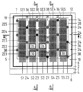
[0022] Figure 1 is a diagram of an LCD display element
according to an embodiment of the invention.
[0023] Figure 2 is a diagram of the layout of the row
electrodes of the embodiment of figure 1.
[0024] Figure 3 is a cross sectional view of the embodiment
of figure 1 along the A-A axis.
[0025] Figure 4 is a cross sectional view of the embodiment
of figure 1 along the B-B axis.
[0026] Figure 5 is a cross sectional view of the embodiment
of figure 1 along the C-C axis.
[0027] Figures 6A-D are schematic diagrams of various views
of an electrical contact point of an LCD display element.
8
CA 02622448 2008-02-26
[0028] Figures 7A-B are schematic diagrams of various views
of an adhesive point of an LCD display element.
[0029] Figures 8A-B are schematic diagrams of various views
of an adhesive point with a row lead that extends into a
spacing area.
[0030] Figures 9A-B are various views of a display panel
including a plurality of LCD display elements that are
arranged flush against one another, side-by-side and one
above the other.
[0031] Figure 1OA-B are various views of a display panel
including a plurality of LCD display elements that are
arranged in the manner of shingles, side-by-side and partly
overlapping one another.
[0032] Figure 11 is a schematic diagram of an LCD display
element according to the prior art.
[0033] Figure 12 is a schematic diagram of another LCD
display element according to the prior art.
DETAILED DESCRIPTION
[0034] Reference will now be made in detail to some
embodiments of the invention, examples of which are
illustrated in the accompanying drawings.
[0035] Figures 1 through 5 are schematic representations of
various embodiments of LCD display elements. Figure 1 shows
a rectangular LCD display element with a first, optically
transparent cover plate 1 and a second optically translucent
9
CA 02622448 2008-02-26
cover plate 2. The two cover plates 1 and 2 are of equal
width. The first cover plate 1 is somewhat longer than the
second cover plate 2, creating a contact margin 4. The edges
of the two cover plates 1 and 2 form a left lateral edge 5, a
right lateral edge 6, an upper lateral edge 7 and a lower
lateral edge B. A liquid crystal 10 is located between the
two cover plates 1 and 2. The optically transparent and
translucent cover plates 1 and 2 are attached to one another,
spaced somewhat apart from one another, by an adhesive rim
12. The liquid crystal 10 is enclosed by the two cover
plates 1 and 2 and the adhesive rim 12.
[0036] A matrix-type electrode assembly 14 is provided
within the boundaries of the adhesive rim 12. The matrix-
type electrode assembly 14 has five strip-type row electrodes
ZE1 through ZE5 and five strip-type, rectangular column
electrodes SE1 through SE5. The column electrodes SE are
arranged within a first plane 16 on the interior side of the
first cover plate 1, and have a first electrode end 18 and a
second electrode end 19. Spacing areas 20 are provided
between the individual column electrodes SE. The spacing
areas 20 electrically insulate the column electrodes SE from
one another. The row electrodes ZE are arranged within a
second plane 22 on the interior side of the second cover
plate 2. The individual row electrodes ZE are electrically
insulated from one another by separation areas 24. The areas
in which the row and column electrodes ZE and SE cross over
one another, with the liquid crystal 10 between them, define
the individual pixels 26 of the LCD display element. The
area of these pixels 26 defines a viewing area 28 in which
information can be optically displayed.
CA 02622448 2008-02-26
[0037] Figure 2 shows that the individual row electrodes ZE
are significantly narrower in the spacing area than in the
crossover or pixel area. Essentially, the individual row
electrodes ZE consist of a plurality of pixel segments 30
that determine the shape of the individual pixels 26. The
pixel segments 30 are electrically connected to one another
via connecting elements 32. The connecting elements 32
alternatingly connect the upper and the lower edges of the
pixel segments 30. An LCD alignment layer 34 is also
arranged on the interior side of the first or second cover
plate. The LCD alignment layer 34 is arranged on top of the
row electrodes ZE and column electrodes SE.
[0038] The row electrodes ZE and column electrodes SE are
activated via row leads Zl through Z5 or via column leads S1
through S5. Both the row leads Z1 through Z5 and the column
leads S1 through S5 are arranged within the first plane 16 on
the interior side of the first cover plate 1. The column
leads SE contact each of the column electrodes SE at their
first electrode end 18. The column leads S1 through S5 are
routed out of the liquid crystal cell through the adhesive
rim 12 to the contact margin 4 in the vicinity of the lower
lateral edge 8. The row leads Zi and Z3 through Z5 are
routed between the column electrodes SE in the spacing areas
20. The row lead Z2 to the second row electrode ZE2 is
routed in the area between the fifth column electrode SE5 and
the adhesive rim 12 near the right lateral edge 6.
Alternatively, the second row lead Z2 can also be routed
under the adhesive rim 12.
[0039] Each of the individual row leads Z1 through Z5
extends within the first plane 16, up to a point underneath
11
CA 02622448 2008-02-26
the connecting element 32 of the row electrode ZE to be
contacted. Each of the individual row leads Z1 through Z5
ends in an electrical contact point 36. The electrical
contact point 36 displaces the liquid crystal 10 from the
first plane 16 to the second plane 22. In the second plane
22, the electrical contact point 36 electrically connects
each connecting element 32 of the corresponding row electrode
ZE to be contacted to the allocated row lead, as shown in
figure 3. The electrical contact points 36 are to be
electrically conductive only in a perpendicular direction to
the cover plates 1 and 2, as opposed to in a parallel
direction to the cover plates. The electrical conductivity
only in a perpendicular direction is indicated in figures 3
and 5 by perpendicular lines 37. The manner in which the
electrical conductivity is achieved in only one direction is
later explained below in reference to figure 6D.
[0040] Figure 1 shows that the first row lead Z1 for
activating the first row electrode ZE1 is positioned between
the third and fourth column electrodes SE3 and SE4. The
third row lead Z3 for activating the third row electrode ZE3
is positioned in the area between the second and third column
electrodes SE3 and SE5. The fourth row lead Z4 for
activating the fourth row electrode ZE4 is positioned in the
area between the first and second column electrodes SE1 and
SE2. The fifth row lead Z5 for activating the fifth row
electrode ZE5 is positioned in the area between the fourth
and fifth column electrodes SE4 and SE5.
[0041] The LCD display element of figure 1 includes adhesive
points 38 that are spaced evenly over the viewing field 28 at
multiple areas in which separation areas 24 and spacing areas
12
CA 02622448 2008-02-26
20 cross over one another. The adhesive points 38 displace
the liquid crystal 10 and connect the two cover plates 1 and
2 to one another in the manner of the adhesive rim 12. The
adhesive points 38 are preferably arranged at crossover areas
between the separation area and the spacing area in which a
row lead in the first plane 16 crosses over a connecting
element 32 of a row electrode in the second plane 22 that is
not to be activated. In this spatial configuration, however,
this small crossover area could potentially be activated with
corresponding activation signals. The adhesive points 38
provided in these areas prevent this. As shown in figure 1,
either an adhesive point 38 or an electrical contact point 36
is preferably positioned at each crossover area between the
separation areas 24 and the spacing areas 20 in which
connecting elements 32 are present. A liquid crystal cell
with a constant distance between the two cover plates 1 and 2
is achieved with the adhesive points 38, which are uniformly
distributed over the viewing field 28 or the LCD display
element. The liquid crystal cell therefore has a liquid
crystal 10 of constant thickness.
[0042] Figure 3 shows a cross sectional view through the
center of the spacing area 20 between the second and third
column electrodes SE2 and SE3 along the line A-A in figure 1.
Figure 4 shows a cross sectional view along the center of the
fourth column electrode SE4 and the allocated fourth row lead
Z4 along the line B-B. Figure 5 shows a cross sectional view
along the upper edge of the third row electrode ZE3 along the
line C-C.
[0043] The illustration of the exemplary embodiment of the
invention in figures 1 through 5 is merely schematic
13
CA 02622448 2008-02-26
representation and is not true to scale. Figures 6 through 8
are drawn more closely to scale and show four exemplary,
directly adjacent pixels 26. The pixels 26 (designated as
pixel segments 30-i) have a rectangular basic shape with
beveled or chamfered corners. The chamfered corners serve to
enlarge the crossover areas between the spacing areas 20 and
the separation areas 24. This creates more space for the
electrical contact points 36 and the adhesive points 38. The
separation areas 24 are approximately 0.05 mm wide and
therefore are much thinner than the approximately 0.3 mm
thick spacing areas 20 in which the row leads Z are routed.
The row leads Z are approximately 0.1 mm wide. The
connecting elements 32-i are also approximately 0.1 mm wide.
The diameter of the adhesive points 38 and the electrical
contact points 36 is approximately 0.35 mm. The individual
pixels 26 have a width of approximately 1.8 mm and a height
of approximately 2.1 mm.
[0044] Figure 6A shows an electrical contact point 36
located between four pixels 26 (designated as pixel segments
30-1 through 30-4) in the area in which a spacing area 20 and
a separation area 24 cross over one another. Figure 6B is an
enlarged view of the electrical contact point 36 of figure
6A. Figure 6C shows a cross section along the line A-A of
figure 6B. Figure 6D shows an enlarged section of figure 6C.
The area shown in figures 6A-D corresponds to the electrical
contact point 36 in figure 1, which connects the fourth row
lead Z4 to the fourth row electrode ZE4. The pixel segments
30-1 and 30-2 are a part of the fifth row electrode ZE5 and
are connected to one another via a connecting element 32-1.
The pixel segments 30-3 and 30-4 are connected to one another
via a connecting element 32-2. The pixel segments 30-3 and
14
CA 02622448 2008-02-26
30-4 are a part of the fourth row electrode ZE4, which is to
be contacted. Consistent with the configuration of
connecting elements 32-i shown in figure 2, the connecting
elements 32-3, 32-4, 32-5 and 32-6 in figure 6A are inserted
diagonally opposite the connecting elements 32-1 and 32-2.
[0045] As was already discussed in the description of
figures 1 through 5, the electrical contact points 36 are
electrically conductive only in a direction perpendicular to
the electrode assembly 14. This is achieved through an
arrangement and configuration of electrically conductive
particles 40 in the electrical contact points 36. The
spacing "d" shown in figure 6D between the interior sides of
the two cover plates 1 and 2 is approximately 5 to 10 pm.
The diameter of an electrical contact point 36, from a plan
perspective, is approximately 0.35 mm as shown in figure 6B.
The conductive particles 40, e.g., in the form of tiny gold
spheres, have an average diameter that is somewhat larger
than the cell gap "d". Thus, the average diameter of the
conductive particles 40 is between 10% and 20% larger than
the spacing "d" between the two cover plates 1 and 2.
Therefore, the conductive particles 40 are clamped and
compressed between the two cover plates 1 and 2 so that a
good electrical contact to the fourth row electrode ZE4 and
the fourth row lead Z4 is created. Figure 6B shows that the
single layer of electrically conductive particles 40 is
statistically distributed over the cross-sectional surface of
the electrical contact points in such a way that an average
distance "D" results between the individual particles 40,
which is substantially larger than their diameter. Thus the
electrical contact points 36 are not electrically conductive
in a direction parallel to the cover plates 1 and 2 (a
CA 02622448 2008-02-26
"transverse" direction) or parallel to the first and second
planes 16 and 22. The fourth row lead Z4 ends precisely
beneath the connecting element 32-2 so that the tiny gold
spheres 40 distributed over the entire cross-sectional
surface of the electrical contact point 36 produce an
electrical contact only between the connecting element 32-2
and the end of the fourth row lead Z4 located directly
beneath it.
[0046] Figures 7A and 7B show an adhesive point 38 between
four pixels 26 (designated as pixel segments 30-1 through 30-
4) in a manner similar to the diagrams in figures 6A through
6D. Figures 7A and 7B correspond to the illustration of the
adhesive point 38 in figure 1 between the third and fourth
column electrodes SE3 and SE4 and the fourth and fifth row
electrodes ZE4 and ZE5 or the third and fourth row electrodes
ZE3 and ZE4.
[0047] Figures 8A and 8B show an adhesive point 38 beneath
which a row lead Z extends. For example, this corresponds to
the adhesive points 38 in figure 1 between the first and
second column electrodes SE1 and SE2 and the second and third
row electrodes ZE2 and ZE3. Alternatively, this corresponds
to the adhesive points 38 in figure 1 between the fourth and
fifth column electrodes SE4 and SE5 and the third and fourth
row electrodes ZE3 and ZE4. Figures 6 through 8 also
indicate exemplary dimensions for the individual pixels 26,
the row leads Z, the spacing areas 20 and the separation
areas 24. It is also apparent that the pixels 26 or the
pixel segments 30-i have a rectangular basic shape, with
chamfered corners. The separation areas 24 can be thinner
and narrower in configuration than the spacing areas 20
16
CA 02622448 2008-02-26
because no leads are routed in the separation areas 24
between the individual row electrodes ZE. The width of the
connecting elements 32 is within the range of the width of
the row leads Z.
[0048] Figures 9A and 9b show an exemplary embodiment of a
display panel that includes eight LCD display elements 42-1
through 42-8. Figure 9A shows a plan view, and figure 9B
shows a side view. Four LCD display elements 42-1 through
42-4 are arranged side by side in a line, flush against one
another. The four other LCD display elements 42-5 through
42-8 are arranged side-by-side in a second line, rotated
180 , also flush against one another and flush against the
first four LCD display elements 42-1 through 42-4. The
contact margins 4 of the individual LCD display elements are
each positioned at the outside, on the upper and lower edges
of the display panel. The routing of the row leads Z allows
the optically inactive margin in the area of the left, the
upper and the right lateral edges 5, 6 and 7 to be thin and
narrow enough in configuration that it is around half the
width of a spacing area 20. Thus, the crossover between two
LCD display elements arranged flush against one another is
nearly optically imperceptible.
[0049] Figures 10A and lOB show an alternative embodiment of
a display panel having a matrix arrangement of individual LCD
display elements 42-i with four rows AZ and three columns AS.
Figure 10A shows a plan view, and figure l0B shows a side
view. The LCD elements 42-i are arranged in a line in the
manner of shingles overlapping one another in the area of the
contact margin 4. The individual rows AZ are arranged flush
against one another, side-by-side. In this manner, nearly
17
CA 02622448 2008-02-26
any size display panel can be produced. The embodiment shown
in figure 10 is especially suitable for use in reflective LCD
display elements having a cholesteric liquid crystal.
[0050] Although the present invention has been described in
connection with certain specific embodiments for
instructional purposes, the present invention is not
limited thereto. Accordingly, various modifications,
adaptations, and combinations of various features of the
described embodiments can be practiced without departing
from the scope of the invention as set forth in the claims.
18