Note: Descriptions are shown in the official language in which they were submitted.
CA 02623157 2008-03-19
PCT/EP2006/064691 - 1 -
2005P12108WOUS
Description
Method for controlling a polyphase converter with distributed
energy stores
The invention relates to a method for controlling a converter
having at least two phase modules, which each have an upper and
a lower valve branch, which each have at least two series-
connected two-pole subsystems, with a constant, freely variable
number of subsystems of each phase module being operated such
that their terminal voltages are in each case equal to a
capacitor voltage across the energy storage capacitor in the
associated subsystem, with the remaining subsystems of this
phase module being operated such that their terminal voltages
are equal to zero.
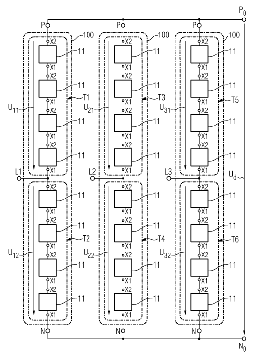
A polyphase converter is known from DE 101 03 031 Al. Figure 1
illustrates a circuit arrangement of a converter such as this,
in more detail. According to this circuit arrangement, this
known converter circuit has three phase modules, which are each
annotated 100. These phase modules 100 are each electrically
conductively connected on the DC voltage side by a respective
connection P or N to a positive and a negative DC voltage
busbar Po and No. There is a DC voltage Ud between these two DC
voltage busbars Po and No. Each phase module 100 has an upper
and a lower valve branch T1, T3 and T5, as well as T4 and T6,
respectively. Each of these valve branches T1 to T6 has a
number of two-pole subsystems 11 which are electrically
connected in series. Four of these subsystems 11 are shown for
each valve branch T1, ..., T6 in this equivalent circuit. Two-
pole subsystems 12 (Figure 3) can also be electrically
connected in series instead of the two-pole subsystems 11
(Figure 2) . Each junction point between two valve branches T1
and T2, T3 and T4 or T5 and T6 of a phase module 100 forms a
respective connection L1, L2 or L3 of this phase module 100
CA 02623157 2008-03-19
PCT/EP2006/064691 - 2 -
2005P12108WOUS
on the AC voltage side. Since, in this description, the
converter has three phase modules 100, a three-phase load, for
example a three-phase motor, can also be connected to their
connections Ll, L2 and L3, which are also referred to as load
connections, on the AC voltage side.
Figure 2 shows one embodiment of a two-pole known subsystem 11
in more detail. The circuit arrangement shown in Figure 3
represents a functionally completely equivalent variant, which
is likewise known from DE 101 03 031 Al. These known two-pole
subsystems 11 and 12 each have two semiconductor switches 1, 3
and 5, 7 which can be switched off, two diodes 2, 4 and 6, 8,
and a unipolar energy storage capacitor 9 and 10. The two
semiconductor switches 1 and 3, as well as 5 and 7,
respectively, which can be switched off are electrically
connected in series, with these series circuits being connected
electrically in parallel with a respective energy storage
capacitor 9 or 10. One of the two diodes 2, 4 and 6, 8 is
electrically connected in parallel with each semiconductor
switch 1 and 3, or 5 and 7, respectively, which can be switched
off such that these diodes 2, 4 and 6, 8 are electrically
connected back to back in parallel with the corresporiding
semiconductor switches 1, 3, 5 or 7 which can be switched off.
The unipolar energy storage capacitor 9 or 10 in the respective
subsystem 11 or 12 comprises either a capacitor or a capacitor
bank composed of a plurality of such capacitors with a
resultant capacity Co. The connecting point of the emitter of
the respective semiconductor switch 1 or 5 which can be
switched off and the anode of the respective diode 2 or 6 forms
a connecting terminal X1 of the respective subsystem 11 or. 12.
The connecting point of the two semiconductor switches 1 and 3
which can be switched off and of the two diodes 2 and 4 form a
second connecting terminal X2 of the subsystem 11. The
connecting point of the collector of the semiconductor switch 5
which can be switched off and the cathode of the diode 6 forms
a second connecting terminal X2 of the subsystem 12.
CA 02623157 2008-03-19
PCT/EP2006/064691 - 2a -
2005P12108W0US
In both illustrations of the embodiments of the two subsystems
11 and 12, as illustrated in Figures 2 and 3, insulated gate
bipolar transistors (IGBTs) are used as semiconductor switches
1, 3 and 5, 7 which can be switched off. Furthermore,
CA 02623157 2008-03-19
PCT/EP2006/064691 - 3 -
2005P12108WOUS
MOS field-effect transistors, also referred to as MOSFETs, can
be used. Gate turn-off thyristors (GTO thyristors) or
integrated gate commutated thyristors (IGCTs) can likewise be
used as semiconductor switches 1, 3 and 5, 7 which can be
turned off.
According to DE 101 03 031 Al, the respective subsystems 11 and
12 of each phase module 100 of the polyphase converter shown in
Figure 1 can be controlled in a switching state I, II or III,
respectively. In the switching state I, the respective
semiconductor switch 1 or 5 which can be turned off is switched
on, and the respective semiconductor switch 3 or 7 which can be
turned off in the subsystem 11 or 12 is switched off. This
results in a terminal voltage UX21, at the connecting terminals
Xl and X2, in the respective subsystem 11 or 12 being equal to
zero. In the switching state II, the respective semiconductor
switch 1 or 5 which can be turned off is switched off, and the
respective semiconductor switch 3 or 7 which can be turned off
in the subsystem 11 or 12 is switched on. In this switching
state II, the terminal voltage UyZl that occurs is equal to the
capacitor voltage Uc across the respective energy storage
capacitor 9 or 10. In the switching state III, both the
respective semiconductor switches 1, 3 and 5, 7 which can be
turned off are switched off, and the capacitor voltage Uc
across the respective energy storage capacitor 9 or 10 is
constant.
Figure 4 shows a circuit arrangement of a further embodiment of
a subsystem 14, in more detail. This two-pole subsystem 14 was
registered in a prior national patent application with the
official file reference 2005P12105 DE, and has four
semiconductor switches 21, 23, 25 and 27 which can be turned
off, four diodes 22, 24, 26 and 28, two unipolar capacitors 29
and 30 and electronics 32, also referred to in the following
text as the electronic assembly 32. The four semiconductor
switches 21, 23, 25 and 27 which can be turned off are
CA 02623157 2008-03-19
PCT/EP2006/064691 - 3a -
2005P12108WOUS
connected electrically in series. Each of these semiconductor
switches 21, 23, 25 and 27 has a diode 22, 24, 26 and 28
electrically connected back-to-back in parallel with it. One
respective unipolar capacitor 29 or 30 is electrically
connected in parallel with two respective semiconductor
switches 21, 23 and 25, 2~ which can be turned off. The
respective
CA 02623157 2008-03-19
PCT/EP2006/064691 - 4 -
2005P12108W0US
unipolar capacitor 29 or 30 in this subsystem 14 comprises
either a capacitor or a capacitor bank composed of a plurality
of such capacitors with a resultant capacitance Co. The
connecting point of the two semiconductor switches 21 and 23
which can be turned off and of the two diodes 22 and 24 forms a
second connecting terminal X2 of the subsystem 14. The
connecting point of the two semiconductor switches 25 and 27
which can be turned off and of the two diodes 26 and 28 forms a
first connecting terminal X1 of this subsystem 14. The
connecting point of the emitter of the semiconductor switch 23
which can be turned off, of the collector of the semiconductor
switch 25 which can be turned off, of the anode of the diode
24, of the cathode of the diode 26, of the negative connection
of the unipolar capacitor 29 and of the positive connection of
the unipolar capacitor 30 forms a common potential Po M, which
is electrically conductively connected to a reference-ground
potential connection M of the electronics assembly 32. This
electronics assembly 32 is linked for signalling purposes by
means of two optical waveguides 34 and 36 to a higher-level
converter control system, which is not illustrated in any more
detail. The common potential PoM is used as a reference ground
potential for the electronics assembly 32.
This subsystem 14 can be controlled in four switching states I,
II, III and IV. In the switching state I, the semiconductor
switches 21 and 25 which can be turned off are switched on, and
the semiconductor switches 23 and 27 which can be turned off
are switched off. In consequence, the terminal voltage Ux21 at
the connecting terminals X2 and Xl in the subsystem 14 is equal
to the capacitor voltage Uc across the capacitor 29. In the
switching state II, the semiconductor switches 21 and 27 which
can be turned off are switched on while, in contrast, the
semiconductor switches 23 and 25 which can be turned off are
switched off. The terminal voltage Uaz1 of the subsystem 14 now
corresponds to the sum of the capacitor voltages Uc across the
unipolar capacitors 29 and 30. In the switching state III, the
CA 02623157 2008-03-19
PCT/EP2006/064691 - 4a -
2005P12108WOUS
semiconductor switches 23 and 25 which can be turned off are
switched on, and the semiconductor switches 21 and 27 which can
be turned off are switched off. In this switching state, the
terminal voltage Uy,1 of the subsystem 14 is equal to 0. In the
switching state IV,
CA 02623157 2008-03-19
PCT/EP2006/064691 - 5 -
2005P12108WOUS
the semiconductor switches 23 and 27 which can be turned off
are switched on while, in contrast, the semiconductor switches
21 and 25 which can be turned off are switched off. In
consequence, the terminal voltage Uxzl of the subsystem 14
changes from the potential level "zero" to the potential level
"capacitor voltage Uc:" which is the voltage across the unipolar
capacitor 30. In the switching states I and IV, the respective
energy store 29 or 30 receives or emits energy depending ori the
terminal current direction. In the switching state III, the
capacitors 29 and 30 receive or emit energy depending on the
terminal current direction. In a switching state III ("zero"),
the energy in the capacitors 29 and 30 remains constant. This
subsystem 14 according to the invention therefore corresponds,
in terms of its functionality, to the known subsystem 11 being
connected in series with the known subsystem 12.
The maximum number of respective energy stores 9 and 10 which
can in fact be connected in series between a positive terminal
P and the connection Lx, where x = 1, 2, 3, on the AC voltage
side of each phase module 100 of the polyphase converter as
shown in Figure 1 is referred to as the series operating
cycle n. The maximum number of respective energy stores 9 and
which are actually connected in series between a positive
terminal p and the connection Lx, where x = 1, 2, 3, on the AC
voltage side is reached when all the subsystems 11, 12 and/or
all the subsystems 14 of this valve branch Tl, T3 or T5 have
been switched to the switching state II (U11 = n- Uc and
U-; = n- Uc and U31 = n- Uc, respectively) . It is advantageous,
but not absolutely essential, to provide the same series
operating cycle n between the connection Lx on the AC voltage
side and a negative terminal N of each phase module 100. The
subsystems 11 and 12 shown in Figures 2 and 3 have a respective
energy storage capacitor 9 or 10, while the subsystem 14 shown
in Figure 4 contains two energy storage capacitors 29 and
CA 02623157 2008-03-19
PCT/EP2006/064691 - 5a -
2005P12108WOUS
30. This therefore results in a series operating cycle of n = 4
for the polyphase converter shown in Figure 1, when four
subsystems 11 and 12 are electrically connected in series in
each case between the positive terminal P and the connection
Lx, on the AC voltage side of each phase module 100. However,
if four subsystems 14 as shown in Figure 4 are connected in
series
CA 02623157 2008-03-19
PCT/EP2006/064691 - 6 -
2005P12108WOUS
between the positive terminal P and the connection Lx on the AC
voltage side of each phase module 100, then this results in a
series operating cycle of n = 8, since eight energy stores 29
and 30 can then be electrically connected in series. In
applications in the field of power distribution, a polyphase
converter such as this with distributed energy stores for each
phase module 100 has at least 20 energy storage capacitors 9,
or 29, 30 connected electrically in series. Converters such
as these are used for high-voltage direct-current transmission
systems (HVDC system) or for flexible AC transmission systems,
so-called FACTS.
The following explanatory notes are based on the assumption
that all the energy stores in the subsystems 11, 12 or 14 of
each valve branch T1, T2: T3, T4 or TS, T6, respectively, of
each phase module 100 of the polyphase converter and shown in
Figure 1 each have the same capacitor voltage Uc. Methods for
initial production of this state and for maintaining it during
operation of a converter such as this are known from
DE 101 03 031 Al.
Figure 5 shows an electrical equivalent circuit of the
polyphase converter shown in Figure 1. In this electrical
equivalent circuit, the individual equivalent circuit
components of each subsystem of a valve branch T1, ..., T6 are
combined to form an electrical equivalent circuit of one valve
branch T1, ..., T6.
In general, it is advantageous to design the polyphase
converter such that, averaged over time, a suitable number of
the systems 11, 12 and/or 14 are always being operated, such
that the sum of their terminal voltages is given by:
Y_ U;;21 = n- Uc (switching state II ). This corresponds to
precisely half of the energy stored in the series-connected
subsystems 11, 12 and/or 14, and leads to a mean intermed=iate-
circuit voltage of Ud = n' Uc. This corresponds to a drive
CA 02623157 2008-03-19
PCT/EP2006/064691 - 6a -
2005P12108WOUS
level b on the DC voltage side of 0.5, with the drive level b
CA 02623157 2008-03-19
PCT/EP2006/064691 - 7 -
2005P12108W0US
representing the ratio of the actual intermediate-circuit
voltage Ud to the maximum possible intermediate-circuit voltage
Uama,. This drive level is calculated using the following
equation:
b = Ua Ud
UamaY 2n'Uc
Equivalent capacitance value of each valve branch T1, ..., T6,
averaged over time, is therefore C/m, where m = n/2. In order
to prevent large uncontrolled equalizing currents flowing
through the DC voltage busbars Po and No between the individual
phase modules 100 of the polyphase converter with distributed
energy stores, the same nominal value is generally
predetermined in each case between the terminals P and N of
each phase module 100 for the respective voltages U11, U12, and
U21, U22, and U31, U32 and this means that:
Ull + UlZ = U21 + Uzz = U31 + U32 = Ud . (2)
If the respective semiconductor switches 1, 3; 5, 7 and 21, 23,
25, 27 of all the phase modules 100 of the polyphase converter
with distributed energy stores are operated in a balanced form,
then, for balancing reasons, the arithmetic mean values of the
valve branch currents ill, i12, izl, i22, i31 and i32 become:
111 - 112 = 121 i22 - 131 - 42 = 1 / 3 ' Id (3)
Because of the effective impedances of the phase modules 100 of
the polyphase converter when the phases are being operated and
loaded in a balanced form, these values are passive. The time
profiles of the valve branch currents ill(t), i12(t), izl(t),
il-2(t), i3,(t) and i32 (t) therefore correspond to the following
equations:
ill (t) - 1/3 Ia + 1/2 iL, (t) ,
il-4 (t) - 1/3 Id + 1/2 iLl (t) ,
CA 02623157 2008-03-19
PCT/EP2006/064691 - 8 -
2005P12108WOUS
i21(t) - 1/3 Id + 1/2 iLZ(t), (4)
i22 (t) - 1/3 Id - 1/2 iLZ (t)
i3l ( t ) - 1/3 Id + 1/2 iL3 (t) ,
i32 ( t ) - 1/3 Id - 1/2 iL3 (t) ,
According to these equations, the valve branch currents ill(t),
i12 (t) , iZl (t) , i (t) , i31 (t) and i32(t) each have corresponding
fundamental profiles comprising a DC component 1/3 Id and an
AC component which corresponds to half the output current
iL,;(t). This combination results from the balanced operation
and the identical impedances, resulting from this, in all the
valve branches Tl, ..., T6 (Figure 5).
In order to ensure the passive setting of these valve branch
currents ill ( t ) , i12 ( t ) , i21 ( t ) , i22 (t) , i31 (t) and i32 (t) the
following rules should be observed with regard to the operation
of the semiconductor switches 1, 3; 5, 7 and 21, 23, 25, 27
which can be turned off in a respective subsystem 11, 12 or 14:
Within one phase module 100, care should always be taken
to ensure that a constant number of energy stores in the
subsystems 11, 12 and/or 14 are connected in series at any
given time.
This means that, when a switching state change occurs from the
switching state I to the switching state II in any given
subsystem 11 or 12, or a change from the switching state I to
II; IV to II; III to IV or III to I in any given subsystem 14,
or from the switching state li to the switching state I in any
given subsystem 11 or 12, or a change occurs from the switching
state II to I; II to IV; IV to III or I to III in any given
subsystem 14 in an upper or lower respective valve branch T1,
T3, T5 or T2, T4, T6 of a phase module 100, a corresponding
switching state change must also take place from the switching
state II to the switching state I of any given subsystem 11 or
CA 02623157 2008-03-19
PCT/EP2006/064691 - 8a -
2005P12108WOUS
12 or a change from the switching state II to I; II to IV; IV
to III or I
CA 02623157 2008-03-19
PCT/EP2006/064691 - 9 -
2005P12108WOUS
to III of any given subsystem 14 or from the switching state I
to the switching state II of any given subsystem 11 or 12 or a
change from the switching state I to II; IV to II; III to IV or
III to I of any given subsystem 14 in a lower or upper
respective valve branch T2, T4, T6 or T1, T3, T5. With a drive
level b of 0.5 on the DC voltage side, this means that. the
subsystems 11, 12 and/or 14 of a phase module 11 must always be
switched such that n and only n energy stores in the subsystems
11, 12 and/or 14 are actually connected in series (Ud = n= Uc).
If this condition is not satisfied, then this leads to
undesirable and uncontrolled equalizing currents between the
phase modules 100 of the polyphase converter with distributed
energy stores as shown in Figure 1. These equalizing currents
are excited by a voltage/time integral 4Uph, which can be
calculated using the following equation:
AUph = k- Uc = AT (5)
In this case, AT is a difference time interval which can occur
when a switching state change occurs. This difference time
interval AT is very much less than 1 s. The factor k is a
constant indicating the difference between the number of energy
stores actually connected in series in the subsystems 11, 12
and/or 14 and the series operating cycle n. If the drive level
b on the DC voltage side is 0.5, then: -n < k_< n. The
equalizing currents which are excited by this voltage/time
integral DUPh can be calculated using the electrical equivalent
circuit shown in Figure 5. In order to prevent high
voltage/time integrals AUph resulting in the excitation of high
equalizing currents, the drive for the polyphase converter with
distributed energy stores should be designed such that only one
or only a small number of subsystems 11, 12 and/or 14 of one
valve branch Tl, ..., T6 can have their switching states
changed at any one time.
CA 02623157 2008-03-19
PCT/EP2006/064691 - 10 -
2005P12108WOUS
This measure limits the constant k to low values.
Basic profiles of the valve branch voltages UXl and Ux2r where
x= 1, 2, of an upper respective valve branch T1, T3 or T5 and
a lower respective valve branch T2, T4 or T6 of a phase module
100 of a polyphase converter with distributed energy stores are
each illustrated, by way of example, in a graph plotted against
time t in Figures 6 and 7. The graph in Figure 8 shows the
profile of the sum of the two valve branch voltages Uyl and Ux?
plotted against time t. In accordance with the control method
described above, the sum of the two valve branch voltages Uxl
and U,;2 is always constant and corresponds to the intermediate-
circuit voltage Ud. The switching operations illustrated in
Figures 6 and 7 are required in order to allow the illustrated
profile of the valve branch voltages Ux1 and UxZ to be set.
These valve branch voltages Ux1 and UX, of a phase module 100
are controlled by a higher-level control system.
According to the known control method, when the number of
energy stores which are actually connected in series in the
upper respective valve branch T1, T3 or T5 is changed, a
corresponding number of subsystems 11, 12 and/or 14 in the
lower respective valve branch T2, T4 or T6 have their switching
state changed such that, in each phase module 100, a constant
number n of energy stores are still connected in series iri the
subsystems 11, 12 and/or 14 for a drive level b of 0.5 on the
DC voltage side. This results in a constant DC voltage of
Ud = n - Uc.
If this known method is used in all the parallel-connected
phase modules 100 of the polyphase converter with distributed
energy stores, this generally leads to there being no
significant equalization processes in the form of equalizing
currents between these phase modules 100. However, this is also
dependent on the impedance relationships illustrated in
Figure 5.
CA 02623157 2008-03-19
PCT/EP2006/064691 - 11 -
2005P12108W0US
The invention is now based on the idea of being able to
influence the valve branch currents ill, il , i21, i 2, i31 and i32
differently from their passively set profile.
In principle, additional valve branch currents iZXY(t) can be
set and controlled as required in each valve branch T1, T2; T3,
T4 or T5, T6, respectively, in a time profile for a valve
branch current ill (t) , i12 (t) , i21 (t) , i22 (t) , i31 (t) and i37 (t) .
These additional valve branch currents iZxy(t) result in the
time profiles of the valve branch currents, according to
equation system (4), becoming:
i11 (t) = 1/3 Id + 1/2 iLl(t) + iZ11 (t) i
i12 ( t ) = 1/3 Id + 1/2 iLl ( t ) + iZ12 (t) ,
i21 ( t ) = 1/3 Id + 1/2 iL2 ( t ) + iZ21 (t) , (6)
i22 ( t ) = 1/3 Id + 1/2 1L2 ( t ) + 1Z22 (t) ~
131 (t) = 1/3 Id + 1/2 1L3 (t) + 1Z31 (t) i
132 (t) = 1/3 Id + 1/2 1L3 (t) + 1Z32 (t)
In order to ensure that the output currents iLx(t) do not
change, the additional valve branch currents iZ,y(t) are set
such that the additional valve branch currents iZXy(t) of each
phase module 100 are the same. This means that:
iZ11 (t) = iZ12 (t)
iZ12 ( t ) = iZ22 (t) , (7)
1Z31 ( t ) = 1Z32 (t) ~
The invention is now based on the object of developing the
known control method for a polyphase converter with distributed
energy stores such that predetermined additional valve branch
currents occur.
According to the invention, this object is achieved by the
features of claim 1 or claim 5.
CA 02623157 2008-03-19
PCT/EP2006/069691 - 11a -
2005P12108WOUS
Since additional voltage/time integrals are used in the valve
branch voltages of a phase module
CA 02623157 2008-03-19
PCT/EP2006/064691 - 12 -
2005P12108W0US
as a manipulated variable to influence the valve branch
currents, the valve branch currents can be influenced
deliberately.
Voltage/time integrals such as these are produced, according to
the invention, by the switching operations in the two valve
branches of each phase module of the polyphase converter with
distributed energy stores no longer being carried out
synchronized in time, but with a freely variable time interval.
Voltage/time integrals such as these are also produced
according to the invention by providing a further switching
operation between the switching operations which are
synchronized in time.
These further switching operations can be carried out in an
upper and/or a lower valve branch of each phase module of the
polyphase converter with distributed energy stores. This
results in a balanced drive at the times of the additional
switching operations in the upper and/or lower valve branches
of each phase module of the polyphase converter with
distributed energy stores.
In one advantageous method, the switching operations of an
upper valve branch of a phase module are carried out delayed
and/or advanced with respect to switching operations of a lower
valve branch of this phase module. This allows a predetermined
additional voltage/time integral to be set dynamically over one
period of the valve branch voltages of a phase module.
In a further advantageous method, the two methods are combined
with one another in order to generate additional voltage/time
integrals. This means that a required predeterrnined
voltage/time integral can be generated at any desired time.
CA 02623157 2008-03-19
PCT/EP2006/064691 - 13 -
2005P12108WOUS
A valve branch current can in each case be calculated as a
function of the additional voltage/time integrals in
conjunction with the electrical equivalent circuit of the valve
branches of the polyphase converter with distributed energy
stores. If the valve branch currents of the individual phase
modules of the polyphase converter with distributed eriergy
stores are measured, then an additional voltage/time integral
can be determined at any time, ensuring that the existing valve
branch currents are changed such that equalizing currents can
no longer flow between the phase modules of the polyphase
converter with distributed energy stores.
The use of the control method according to the invention
results in dynamic control of the valve branch currents of a
polyphase converter with distributed energy stores. Inter alia,
this use results in a number of advantages:
- damping of current oscillations, for example caused by:
- transient load change processes
- faults, for example unbalances in a power supply
system or a machine, ground faults, lightning
strikes, switching overvoltages, ...
- inadequate damping of capacitive networks by the
inductances and resistances provided in the design.
- Faults coped with better.
- Poor operating points coped with such as:
- operating points at low output frequencies.
- Capabilities to optimize the design of the subsystems
and of the polyphase converter in terms of capacitor
complexity and the need for power semiconductors.
- A uniform load ensured on all semiconductor switches
which can be turned off.
CA 02623157 2008-03-19
PCT/EP2006/064691 - 14 -
2005P12108W0US
- Balancing of highly unbalanced voltage on the
individual converter elements after fault
disconnection.
The rest of the explanation of the invention refers to the
drawing, which schematically illustrates a plurality of
embodiments of one method according to the invention for
controlling a polyphase converter with distributed energy
stores, and in which:
Figure 1 shows a circuit arrangement of a known converter with
distributed energy stores,
Figures 2 to 4 each show a circuit arrangement of one
embodiment of a known subsystem,
Figure 5 shows an electrical equivalent circuit of the valve
branches of the converter shown in Figure 1,
Figures 6 and 7 each use a graph plotted against time t to show
a valve branch voltage of an upper and lower valve
branch of a phase module of the known converter shown
in Figure 1,
Figure 8 uses a graph plotted against time t to show the sum
voltage of the two valve branch voltages shown in
Figures 6 and 7,
Figures 9 and 10 each use a graph plotted against time t to
show the valve branch voltages of a phase module of
the converter shown in Figure 1, when using a first
embodiment of the control method according to the
invention,
Figure 11 uses a graph plotted against time t to show the sum
voltage of the two valve branch voltages shown in
Figures 9 and 10,
Figures 12 and 13 each use a graph plotted against time t to
show valve brarich voltages of a phase
CA 02623157 2008-03-19
PCT/EP2006/064691 - 15 -
2005P12108WOUS
module of the converter shown in Figure 1 when using
a second embodiment of the control method according
to the invention,
Figure 14 uses a graph plotted against time t to show the
associated sum voltage,
Figures 15 and 16 each use a graph plotted against time t to
show a valve branch voltage of a phase module of the
converter shown in Figure 1, with these being the
valve branch voltages which occur when using a
combination of the two embodiments of the control
method according to the invention, and
Figure 17 shows a graph plotted against time t of the
associated sum voltage.
The graph in Figure 9 shows the profile of a valve branch
voltage UXl of an upper valve branch Tl, T3 and T5 of a phase
module 100 of the converter shown in Figure 1, plotted against
time t. The time profile of a valve branch voltage UxZ of a
lower valve branch T2, T4 or T6 of this phase module 100 is
illustrated in more detail in the graph in Figure 10. The sum
voltage of these two valve branch voltages Uxl and Ux2 of a
phase module 100 of the converter shown in Figure 1 is
illustrated, plotted against time t, in the graph in Figure 11.
If this sum voltage is compared with the sum voltage in
Figure 8, it is evident that the sum voltage shown in Figure 11
has additional voltage/time integrals AUpnlf ... , DUpn9 = These
additional voltage/time integrals AUp;,l, ..., AUph4 occur
because the switching operations in the upper and lower
respective valve branches T1 and T2; T3 and T4 as well as T5
and T6 of a phase module 100 are no longer carried out
synchronized in time. Any given subsystem 11, 12 changes from
the switching state I to the switching state II at the time tl,
or any given subsystem 14 in the lower respective valve branch
T2, T4 or T6 of the phase module 100 changes from the switching
state I to II or IV to II, or III to IV, or III to I at the
time tl in comparison to the change of the switching state II
CA 02623157 2008-03-19
PCT/EP2006/064691 - 16 -
2005P12108WOUS
to the switching state I of any given subsystem 11, 12 or the
change from the switching state II to I, II to IV, IV to III,
or I to III of any given subsystem 14 in the upper respective
valve branch T1, T3 or T5 of this phase module 100, delayed by
a time interval 4T1. The additional voltage/time integral AUPf,l
resulting from this is calculated using the following equation:
dUPn = k- Uc - ATz (8)
In this case, the factor k indicates the difference between the
energy stores (in the switching state II in subsystems 11, 12
and in the switching state I or I I or IV in the subsystem 14)
which are actually connected in series and through which
current passes during the time interval 4Tzr and the series
operating cycle n. In this example, the series operating cycle is
n = 4. This results in a factor of k=-1 for the time interval
4T1. At the time t4, any given subsystem 11, 12 changes from the
switching state I to the switching state II, or any given
subsystem 14 in the upper valve branch Tl, T3 or T5 changes from
the switching state I to II, IV to II, III to IV, or III to I,
with an advance corresponding to the time interval AT2 with
respect to any given subsystem 11, 12 changing from the
switching state II to the switching state I or any given
subsystem 14 in the lower valve branch T2, T4, or T6 changing
from the switching state II to I, II to IV, IV to III or I to
III. The factor is therefore k = +1 during the time interval
AT2. The magnitude of the additional voltage/time integrals
AUP!,1r ..., DUPh9 can be determined using the freely variable time
interval 4TZ. The mathematical sign of the additional
voltage/time integral DUPh and therefore the mathematical sign
of an additional valve branch current izr},(t) are determined by
means of the factor k. The additional valve branch current
izx}.(t) can be varied by generating a plurality of additional
voltage/time integrals AUPh distributed over the period of the
fundamental frequency of the valve branch voltage U,l or U,,,
CA 02623157 2008-03-19
PCT/EP2006/064691 - 16a -
2005P12108WOUS
respectively, of a respective upper or lower valve branch T1,
T3, T5 or T2, T4, T6. The valve branch currents iYy(t)
CA 02623157 2008-03-19
PCT/EP2006/064691 - 17 -
2005P12108WOUS
can be dynamically controlled by means of this method according
to the invention for controlling a polyphase converter with
distributed energy stores as shown in Figure 1.
The graph in Figure 12 shows the profile of a valve branch
voltage U,;l of an upper valve branch T1, T3 or T5 of a phase
module 100 of a converter shown in Figure 1. The profile of a
valve branch voltage U,t2 of a corresponding respective valve
branch T2, T4 or T6 of this phase module 100 is plotted against
time t in the graph in Figure 13. The associated sum voltage of
these two valve branch voltages Ux1 and Ux2 is illustrated
plotted against time t in the graph in Figure 14. These two
valve branch voltages Uxl and UXz differ from the two valve
branch voltages U,.1 and Uxz shown in Figures 6 and 7 by
additional switching operations being carried out in addition
to the switching operations that are synchronized in time. Two
switching operations have been inserted in the profile of the
valve branch voltage UX1 in the time period t2 - tl, resulting
in connection of a further respective subsystem 11 or 12 or a
further energy store of a subsystem 14 of the respective upper
valve branch T1, T3 or T5 of a phase module 100 for a time
interval 4T1. Further switching operations such as these are
carried out in the time period t5 - t4 for a time interval 4T2.
Two switching operations have been inserted in the profile of
the valve branch voltage U,;z in the time period t8 - t7. These
switching operations result in two respective subsystems 11 and
12 or two respective energy stores in the subsystems 14 being
turned off for a time interval AT3 in the lower valve branch
T2, T4 or T6, respectively, of a phase module 100. In the time
period t11-t10, respective further switching operations are
carried out in the upper and lower valve branch T1, T3, T5 and
T2, T4, T6. As a result of these switching operations, a
respective subsystem 11 or 12 or an energy store in a subsystem
14 of a phase module 100 is turned off for this time interval
AT4 in the upper respective valve branch T1, T3 or T5 and a
respective subsystem 11 or 12 or an energy store in a subsystem
CA 02623157 2008-03-19
PCT/EP2006/064691 - 17a -
2005P12108WOUS
14 is likewise turned off for the same time interval AT4 iri the
lower respective valve branch T2, T4 or T6. These further
switching operations in the upper
CA 02623157 2008-03-19
PCT/EP2006/064691 - 18 -
2005P12108WOUS
and/or lower valve branches T1, T3, T5 and/or T2, T4, T6 result
in additional voltage/time integrals DUph1, . . . , DUph9 being
generated, which each generate additional valve branch currents
iZ,,},(t) in the respective valve branches T1, T2; T3, T4 or T5,
T6 of each phase module 100 of the converter shown in Figure 1.
These additional voltage/time integrals DUphl, ..., AUphq can be
obtained from the sum voltage of the two valve branch voltages
U,,1 and Ur2. The magnitude of these additional voltage/time
integrals DUphl, . . . , AUph4 depends on which additional valve
branch currents iZ,y (t) are required in the respective valve
branches T1, T2; T3, T4 or T5, T6 of each phase module 100.
These additional voltage/time integrals AUphl, . . . , DUphq are
calculated using the equation (7) . The additional voltage/time
integrals 4Uph1r . . . , DUpi-,4 obtained from this can also be
distributed over time over one period of the fundamental
frequency of the valve branch voltage Ux1 or Ux2, respectively,
in the method for additionally introduced switching operations.
A combination of the methods for producing additional
voltage/time integrals AUphl, ..., DUphq by delayed and/or
advanced switching operations with additional switching
operations leads to the profiles of the valve branch voltages
U,,1 and U,;Z of an upper and lower respective valve branch Tl,
T2; T3, T4 or T5, T6 of a phase module 100 of the converter
shown in Figure 1. These valve branch voltages Uxl and U,t2 are
respectively shown in a graph plotted against time t in
Figures 15 and 16. An associated sum voltage of these valve
branch voltages Uxl and UYZ plotted against time is illustrated
in the graph in Figure 17.