Note: Descriptions are shown in the official language in which they were submitted.
CA 02623285 2008-03-20
WO 2007/035849 PCT/US2006/036767
1
TITLE OF THE INVENTION
ELECTRICAL STIMULATION OF CELL AND TISSUE GROWTH WITH TWO- AND
THREE-DIMENSIONALLY PATTERNED ELECTRODES
RELATED APPLICATIONS
[0001] This application claims priority to U.S. Provisional Patent Application
No.
60/719,236, filed September 21, 2005.
FIELD OF THE INVENTION
[0002] The present invention generally relates to a device and method for
electrically regulating cellular and/or tissue physiology using a patterned
electric field or
current. The present invention further relates to a device for carrying out
the regulatory
method as well as methods for fabricating the device.
BACKGROUND OF THE INVENTION
[0003] The effect of electrical stimulation on healing and cell growth has
been
explored for decades. Clinical studies have shown improved fracture healing by
using
electric and electromagnetic fields as early as the 1970s. Disk electrodes
coupled to the
skin via conductive gel have been developed that generate and deliver a broad,
noninvasive, capacitively coupled, and uniform electric field to the fracture
site. The
problem with conventional externally generated fields is that they cannot be
directed
preferentially to the fracture site, but rather are generally directed to
large regions of an
organism. Moreover, since the fields produced by conventional external
electrodes are
ordinary dipole fields the field strength diminishes with distance from the
surface of the
electrode. Thus, higher powers are required in order to deliver an effective
field
strength to the target cells.
[0004] Other art overcomes this problem by using implantable electrodes to
localize the field, thus electrical regulation could be carried out in
specific locations more
efficiently, i.e. with waveforms having lower amplitudes and/or frequencies.
This work
used electrodes made from polymer-coated metals such as fluorocarbon-coated
steel.
CA 02623285 2008-03-20
WO 2007/035849 PCT/US2006/036767
2
However, such electrodes are not biodegradable/bioabsorbable therefore they
require
an additional surgery to remove them. Thus, the art is deficient in that it
lacks an
external electrode that is capable of delivering a localized electric field or
current.
Furthermore, the art lacks a biodegradable/bioabsorbable implantable device
for
generating therapeutic electric fields and/or currents.
[0005] The present invention fills this gap in the art by using patterned
electrodes
to create fields that -are capable of being localized preferentially on the
region of the
organism where electric field or current delivery is indicated. Moreover, such
electrodes ~
can be made from conductive polymers (CP) that are
biodegradable/bioabsorbable.
Thus, the electrodes of the present invention can be implanted into an
organism for
therapeutic purposes, without requiring additional surgery to remove the same
when the
therapy is complete. Accordingly, the present invention fills a substantial
gap in the art,
and is novel, non-obvious and deserves broad patent protection.
SUMMARY OF THE INVENTION
[0006] The present invention generally relates to a method for electrically
regulating the physiology of a variety of cell types in vivo or in vitro. More
particularly,
the present invention relates to a method for up-regulating or down-regulating
cellular
processes including without limitation cell growth, metabolic processes,
biological
product production, and tissue healing and regeneration through the use of
patterned
electrodes, which deliver a patterned electric field. The present invention
also relates to
a device for carrying out the regulatory method as well as a method for
fabricating the
device.
[0007] The present invention generally relates to a method for regulating
cellular
and tissue physiology comprising the steps of providing at least one
electrode, providing
at least one cell, placing the electrode in electrical communication with the
at least one
cell, and applying a voltage to the electrode thereby delivering an effective
amount of a
patterned electric field or current to the at least one cell, whereby the
patterned electric
field or current regulates the physiology or growth of the at least one cell.
CA 02623285 2008-03-20
WO 2007/035849 PCT/US2006/036767
3
[0008] The present invention also generally relates to a device for regulating
cellular and tissue physiology comprising at least one electrode. capable of
delivering an
effective amount of a patterned electric field or current to a locus where
dosing is
indicated. Additionally, the present invention relates to a process for
fabricating a
patterned electrode for regulating cellular and tissue physiology comprising
the steps of
providing a nonconductive substrate, providing a conductive material, and
applying the
conductive material to the substrate in a manner that forms a patterned
conductive film
adhering to the substrate.
BRIEF DESCRIPTION OF THE FIGURES
[0009] Figure 1 is a diagram showing a synthetic route to a series of
biocompatible conducting polymers (CPs) with different
sulfonation ratios;
[0010] Figure 2 is a photograph comparing cell growth on standard glass and on
synthesized sulfonated polyaniline;
[0011] Figure 3 is a graph showing the effect of growing cells on different
substrates including non-coated sulfonated polyaniline and PLA
coated polyaniline;
[0012] Figure 4 is an illustration showing the steps of making interdigitated
electrodes from conductive polymers by printing and in-situ
polymerization;
[0013] Figure 5 is a pair of photographs demonstrating the resolution that is
possible with a sophisticated laser printer as compared to an
ordinary laser printer;
[0014] Figure 6 is an illustration showing the steps of using soft lithography
(e.g.
stamping) to fabricate a two dimensionally patterned electrode;
[0015] Figure 7 is an iliustration showing the method of micro molding in
capillaries (MIMIC);
CA 02623285 2008-03-20
WO 2007/035849 PCT/US2006/036767
4
[0016] Figure 8 is a diagram showing the steps of fabricating two
dimensionally
patterned electrodes by positive lithography and lift-off;
[0017] Figure 9 is a group of images including SEMs and photographs of
interdigitated electrodes made from conductive polymers using
positive lithography and lift-off;
[0018] Figure 10 is an illustration of an apparatus for electrical stimulation
of bone
cells on a patterned electrode;
[0019] Figure 11 is a graph showing the voltage dependency of cells growing on
IDE 100 under DC electrical stimulation;
[0020] Figure 12 is a graph showing the relationship between the insulating
layer
thickness and cell growth on IDE50 under DC electrical
stimulation;
[0021] Figure 13 is a set of images showing the effect of electrical
stimulation on
distribution of cells grown on IDE 100;
[0022] Figure 14 is a set of graphs showing the dielectric properties of an
insulating layer of PLA;
[0023] Figure 15 is a pair of graphs showing the electrical properties of an
example SPAN formulation;
[0024] Figui-e 16 is a table setting forth the dimensions of several
interdigitated
embodiments fabricated by printing and in situ polymerization;
[0025] Figure 17 is a pair of plots showing the isopotential and electric
field lines
of an example electrode;
[0026] Figure 18 is a pair of plots showing the potential distribution and
electric
field lines of an example electrode; and
[0027] Figure 19 is a set of plots and a data table showing the effect of
applied
electric field on cell membrane permeability in a dye uptake
study.
CA 02623285 2008-03-20
WO 2007/035849 PCT/US2006/036767
DETAILED DESCRIPTION
[0028] The present invention generally relates to a method for electrically
regulating the physiology of a variety of cell types in vivo or in vitro. More
particularly,
the present invention relates to a method for up-regulating or down-regulating
cellular
processes including without limitation growth, metabolic processes, biological
product
production, and tissue healing and regeneration through the use of patterned
electrodes, which deliver a patterned electric field. The present invention
also relates to
a device for carrying out the regulatory method as well as a method of
fabricating the
device.
[0029] The term electricai communication, as used herein, includes
communication of static and dynamic electric fields, electromagnetic
radiation, and
electric current.
[0030] The term electrode, as used herein encompasses both the singular and
plural forms. Thus, statements regarding "an electrode" apply equally to a
plurality of
electrodes.
[0031] The term 2-dimensionally patterned electrodes, as used herein, includes
a
conductive pattern that substantially extends in two mutually orthogonal
dimensions that
are generally parallel to a non-conductive substrate. Furthermore, although 2-
dimensionally patterned electrodes necessarily include a third spatial
dimension, such
third dimension is merely a thickness.
[0032] The term 3-dimensionally patterned electrodes, as used herein, includes
a
set of 2-dimensionally patterned electrodes that are generally stacked one on
top of the
other so that their fields superposition. Generally, the stack comprises
layers of 2-
dimensionally patterned electrodes that can be separated by intervening
dielectric
layers. Furthermore, the patterned layers can be the same or different
patterns, and
can be aligned or offset in any of a variety of ways. For instance, the
patterns can be
rotationally offset by any number of degrees. Alternatively, the patterns can
be linearly
offset by any appropriate distance. In a still further alternative, the
patterns may be
offset so that the layers are no longer paraliel. Any combination of the
foregoing offsets
is also within meaning of the term 3-dimensionally patterned electrode as used
herein.
CA 02623285 2008-03-20
WO 2007/035849 PCT/US2006/036767
6
Electrically regulated processes
[0033] According to the present invention subjecting many kinds of cells to a
patterned electric field or current enables regulation of a variety of
physiological cellular
and tissue processes including without limitation stimulating cellular
proliferation,
healing and/or regeneration. Other examples of physiological processes that
can be
regulated by the application of a patterned electric field or current include,
without
limitation, ion channel function, secretory processes, chemical absorption
processes,
anabolic and catabolic processes, mass transport processes, cell membrane
permeability, gene product production, cell division and the like. In one
embodiment,
cell permeability is increased by applying an electric field of the present
invention. An
example of this permeability effect can be seen in dye uptake studies as shown
in
Figure 19.
[0034] The physiological processes of a wide variety of cells and tissues can
be
regulated by applying a patterned electric field or current. Such cells
include, but are
not limited to, bone cells including osteoprogenitor and/or stem cells, blood
cells,
cardiac cells, muscle cells, nerve cells, and skin or vascular cells including
epidermal
and endothelial cells, respectively.
[0035] Although there is a clear relationship between voltage and bone growth,
it
is not linear. Rather, the rate at which bone growth increases with increasing
voltage
slows down noticeably at higher voltages. Several plausible explanations
exist. Some
evidence suggests that as cell concentration increases and, more importantly,
as the
number of cells adhering to the electrode increases, the field experienced by
the bulk
cells diminishes due to an screening effect caused by cells at the electrode
surface.
More particularly, according to this line of reasoning the membranes of the
surface-
adherent cells insulate the bulk cells from at least a portion of the field.
Another
explanation may be contact inhibition. That is, when cell density becomes
relatively
high, the competition for limited sources of nutrients and space causes cell
growth to
slow even as higher voltages are applied.
[0036] According to a third theory, an applied voltage may affect the
concentration of cellular growth factors, thereby influencing cellular
proliferation.
CA 02623285 2008-03-20
WO 2007/035849 PCT/US2006/036767
7
Another theory focuses on the behavior of human ceils in response to a pulsed
electromagnetic field (PEMF). Still another theory states that the electric
field induces
expression of one or more growth factors by a mechanism involving the
calcium/calmodulin pathway. Another theory says that the field affects voltage-
sensitive
transmembrane ion channels thereby increasing the influx of calcium ions and
triggering
a series of events including increased cellular proliferation. Any one of the
foregoing
theories or any combination thereof can explain why the relationship between
bone
growth and applied voltage or field strength is non-linear. Regardless of the
precise
explanation, the relationship between bone healing/regeneration and electrical
stimulation is widely recognized.
Electric Fields
[0037] Electric fields within the scope of the present invention include,
without
limitation, constant fields (e.g. DC) including bipolar DC fields, time-
varying fields (e.g.
AC) and any combination thereof. When AC and DC fields are combined, the DC
field's
magnitude can be smaller than, equal to, or greater than that of the AC field.
Additionally, where AC and DC fields are combined the polarity of the DC field
can be
varied. Frequency dependant fields can have any of a variety of appropriate
wave
forms including, but not limited to, square, sinusoidal, triangular,
trapezoidal, or more
complex patterns. Furthermore, appropriate fields can be inductively coupled,
capacitively coupled, and the like. The field can also be pulsed or
continuous. Fields
within the scope of the present invention can be modulated in any of a variety
of ways
including temporally and spatially. Preferably, fields within the scope of the
present
invention can be localized on particular areas of the body so as to
preferentially regulate
cellular and/or tissue physiological processes in particular locations. More
preferably,
fields within the scope of the present invention can be localized on
individual cells or
small collections of cells. In one embodiment field strength can be maximal at
the
surface of an electrode such as a 2-dimensionally patterned electrode. In
another
embodiment field strength can be maximal at a distance from the surface of an
electrode, such as a 3-dimensionally patterned electrode.
[0038] According to the present invention cellular and tissue physiological
processes respond differently depending on field strength. In one non-limiting
example,
CA 02623285 2008-03-20
WO 2007/035849 PCT/US2006/036767
8
higher field strengths tend to result in greater bone growth in terms of
proliferation
(Figures 11 and 12) as well as alkaline phosphatase activity and calcium
deposition.
However upon a higher voltage, the increase slowed down (Figure 11), which may
be
attributed to overconfluence caused contact inhibition or insulating
properties of cellular
membranes.
Electrodes
[0039] Electrodes within the scope of the present invention can take on any of
a
variety of appropriate conformations including without limitation 2-
dimensionally
patterned, and 3-dimensionally patterned electrodes. Patterns within the scope
of the
present invention include, without limitation, interdigitated designs,
parallel lines,
concentric circles, or any of a variety of circumscribed regular or irregular
shapes. In
any case, the sign of the electrode features should alternate in some
appropriate
manner. For instance, with regard to concentric circles one appropriate manner
is that
each successive circle has the opposite sign of the one inside and outside of
it. In
another embodiment, some circles may have the same sign as the circle inside
or
outside or both inside and outside. The other alternative shapes mentioned
above can
alternate in a similar manner. For instance, in an interdigitated embodiment,
one set of
digits is positive and the other set is negative. Some non-limiting examples
of
interdigitated embodiments are set forth in Figure 16.
[0040] With regard to spacing between the features of 2-dimensionally
patterned
electrodes, any of a variety of spacings can be appropriate provided the
resulting
pattern produces a patterned field or current that can be directed to
individual cells or
small collections of cells. The spacing between pairs of features can be
constant
across all or a portion of the electrode. Additionally, the spacing can vary
from one pair
of features to another, and/or along one pair of features. Feature spacings
that are
within the scope of the present invention include, without limitation, from
about 10 nm to
about 200 m. Feature spacings within the scope of the present invention also
include,
without limitation, from about 100 nm to about 100 pm. Feature spacings within
the
scope of the present invention also include, without limitation, from about 1
pm to about
100 pm. Feature spacings within the scope of the present invention also
include,
without limitation, from about I pm to about 100 pm.
CA 02623285 2008-03-20
WO 2007/035849 PCT/US2006/036767
9
[0041] The feature spacing mentioned above enables the present invention to
produce electric fields or currents that are capable of controlling or
regulating cellular
and/or tissue physiological processes. In general, smaller feature spacings
result in
finer control over field strength variations. Thus, a smaller feature spacing
is required to
affect the physiological processes of a single cell than that of a collection
of cells.
Similarly, different feature spacings can be used to affect the physiological
process of
cells of different sizes.
[0042] As mentioned above, 3-dimensionally patterned electrodes are
essentially
a set of 2-dimensionally patterned electrodes that are packed in a multilayer
fashion so
that the field, in a specific location, generated from one layer could be
either cancelled
or enhanced by the field generated from other layers. This type of electrode
pattern
enables the present invention to have maximal field strength at a distance
from the
surface. This is in contrast to 2-dimensionally patterned electrodes, which
have
maximum field strength at the surface. Thus, 3-dimensionally patterned
electrodes
produce a patterned electric field or current similar to that of 2-
dimensionally patterned
electrodes, but also enable the present invention to apply the patterned field
at
maximum strength to a cell or cells located a distance from the electrode.
More
particularly, this kind of electrode can be more efficiently used as an
external (i.e. non-
implanted) electrode. However, 2- and 3-dimensionally patterned electrode can
both be
either implanted or external.
[0043] In one embodiment, a 3-dimensionally patterned electric field can also
be
generated by simply wrapping the targeted area with the 2-dimensionally
patterned
,electrode.
[0044] In addition to 2- and 3-dimensional patterning, the electrode of the
present
invention can have a controlled surface roughness, which can affect cell
adhesion. In
general, cells tend to adhere to rougher surfaces better than smoother
surfaces. Thus,
it may be desirable to include a surface roughness feature in a controlled
manner. In
one embodiment, surface roughness is produced in a controlled manner by adding
a
dielectric coating having a textured surface, or by adding a dielectric layer
and then
creating a texture on the layer, for instance, using a template. In another
embodiment
CA 02623285 2008-03-20
WO 2007/035849 PCT/US2006/036767
surface roughness is achieved by patterning the top dielectric layer in
grooves or wells
through stamping (soft-lithography).
[0045] Electric fields consistent with the present invention can be generated
with
any of a variety of implantable electrodes, or external electrodes (i.e. not
implanted).
Such ;electrodes can comprise any conductive material including without
limitation
metals and alloys thereof, dielectric-coated metals and metal alloys such as
fluorocarbon-coated steel or titanium, doped and/or undoped semiconductors,
and
doped and/or undoped conductive polymers. In one embodiment, the present
invention
comprises conductive polymer electrodes. In another embodiment, the present
invention comprises bioabsorbable/biodegradable conductive polymer electrodes.
[0046] Conducting polymers within the scope of the present invention can be
incorporated into the main chain of a copolymer or can be a pendent group or
groups of
a copolymer. Examples of conductive polymers within the scope of the present
invention include without limitation polypyrroles, polythiophenes, and
polyanilines.
Typically, such conductive polymers are doped in a manner that enhances
electrical
conductivity for example Poly(3,4-ethylenedioxythiophene)
poly(styrenesulfonate) (e.g.
Baytron P) and fully sulfonated polyaniline (e.g. NSPAN).
[0047] -In one embodiment the electrodes of the present invention are
fabricated
from a self-doped conductive polymer. The meaning of the term self-doped, as
used
herein, includes conductive polymers wherein the dopant is covalently tethered
to the
polymer, for instance by a linker group. Self-doped conducting polymers can be
used to
form electrode patterns that provide a wide range of effective dopant
concentrations
from about 0.05 to about 1.0 sulfonic acid groups per aniline repeating unit.
Additionally, such polymers mitigate diffusion effects that can harm
performance.
[0048] In one embodiment the electrodes of the present invention are
fabricated
from sulfonated polyaniline (SPAN). One advantage of SPAN is that introducing
SO3H
can improve the water solubility, as well as environmental stability, of
polyaniline without
substantially sacrificing conductivity. Additionally, the electrical and
chemical properties
of SPAN are pH independent over a broad range, which is especially important
in
implantable applications. Furthermore, polyanilines have a wide range of
stable
CA 02623285 2008-03-20
WO 2007/035849 PCT/US2006/036767
11
oxidations states (including teucoemeraldine, emeraidine, and pernigraniline),
a wide
selection of inorganic and organic counter ions, and versatile acid-base and
redox
chemistries. Biomolecuies, such as growth factors, hormones, and enzymes, can
be
incorporated into the conductive polymer electrodes as dopants, thus creating
unique
properties in addition to biocompatibility and electrical activity.
[0049] Any of a variety of known SPAN preparations can be used in connection
with the present invention. For instance, one such preparation can be carried
out as
follows (See Figure 1). Aniline, 0.05 mol, is copolymerized with 0.05 mole
metanilic
acid in 1 M HCI with 0.05 mole ammonium persulfate as oxidant. The reaction is
kept in
ice bath, stirring for about 6 hrs. Then a large excess of acetone is added to
precipitate
the product, which is collected by filtration. After filtering, washing, and
drying the dark
green product is ground into powder and dissolved in N-methyl-2-pyrrolidone
(NMP) at
a concentration of less than I wt%. In order to enhance conductivity and
ensure
electrical continuity, the SPAN film is dip-coated onto a glass slide (2.5 cm
x 2.5 cm)
rather than spin-coated. Excess solvent is removed by drying slowly at room
temperature in a fume hood for 48 hours. The resulting film has a thickness of
approximately 15 5 pm according to profilometry. The electrical properties of
a SPAN
formulation is shown in Figure 15.
Table. I Physical properties of a series of sulfonated polyanilines showing
that
properties can be adjusted through synthetic modifications.
Sample # Monomers* Oxidant** Medium Yield Solubility Conductivity
(S/cm)
AN: MA
7305 0.07mo1:0.03mol APS 0.05 mol 0.2 mol HCI/ 50.73% 0.1
200 ml H20
(7:3) insoluble in
AN: MA 0.2 mol HCI/ water, CH3Cl,
5505 0.05mo1:0.05mol APS 0.05 mol 200 ml H20 55.46% and toluene. 0.08
(5:5) Soluble in
AN: MA DMSO, DMF,
0.2 mol HCI/
3705 0.03mo1:0.07mol APS 0.05 mol 200 ml H20 59.86% and NMP. 0.005
(3:7) Solubility NMP>
AN: MA DMSO=-DMF
0.2 mol HCI/
5510 0.05mo1:0.05mol APS 0.1 mol 200 ml H20 76.78% 0.003
(5:5)
* AN=aniline, MA= metanilic acid
CA 02623285 2008-03-20
WO 2007/035849 PCT/US2006/036767
12
** APS=ammonium persulfate
Table I above demonstrates that conductivity can be adjusted by altering
monomer
ratios.
Patterning and fabricating
[0050] In one embodiment an electrode within the scope of the present
invention
is fabricated by stamping a solution of conductive polymer or precursor(s)
thereof onto
an appropriate substrate. Appropriate substrates include without limitation
electrically
insulating materials. More particularly, such substrates include without
limitation metal
oxide glasses, ceramics, and organic polymers such as
polyethyleneterephthalates,
polyolefins, phenolic polymers and the like.
[0051] Any of a variety of known methods for stamping can be used to fabricate
electrodes of the present invention. For instance, in one embodiment a stamp
is
fabricated as shown in Figure 6. A substrate 600 is coated with a layer of
negative
photoresist 610, and is then exposed to UV radiation through an appropriate
mask
bearing the desired pattern 620. The latent image is developed 630, i.e. the
uncrosslinked photoresist is removed, thereby forming a mold. Then a
prepolymer 640
is added to the mold, cured, and peeled off. The molded polymer peeled from
the mold
comprises the stamp 642. The stamp can now be wetted with conductive polymer
650
and/or precursors thereof and applied to an appropriate substrate 660 thereby
leaving a
stamped image 652,. and forming a stamped electrode 670.
[0052] In another embodiment of the present invention, electrodes can be
fabricated using a capillary micromolding technique and/or apparatus 700. More
particularly, an empty mold 730 is applied to a substrate 710 so that openings
720 of
the mold are exposed as shown in Figure 7. Then a portion of liquid polymer
and/or
prepolymer is contacted with the opening. The liquid is drawn into the mold by
capillary
forces, which distribute the liquid throughout the mold. The liquid is allowed
to dry
and/or cure and then the mold is removed from the substrate leaving behind a
patterned
conductive polymer film 740.
[0053] In still another embodiment electrodes of the present invention are
fabricated by printing conductive polymer and/or prepolymer directly onto an
appropriate
CA 02623285 2008-03-20
WO 2007/035849 PCT/US2006/036767
13
substrate. In one example an ordinary laser printer is used in combination
with specially
formulated ink to form a patterned conductive polymer film. An appropriate ink
formulation can comprise a conductive polymer and/or prepolymer thereof.
Additionally,
such an ink may optionally comprise a binder, a surfactant, and/or an
oxidizing agent
such as ferric ethylbenzene sulfonate. In one example of this embodiment, a
substrate
coated with an appropriate ink is exposed to excess monomer vapor thereby
developing
the image in the regions containing oxidizing agent. This results in a
conductive
polymer image.
[0054] Another embodiment involves using a laser printer to print a negative
image 400 of an electrode as shown in Figure 4. The negative is then dipped
into a
conductive polymer deposition/coating system. This results in polymer coating
both the
negative image and the exposed substrate. Then the image is developed by
removing
the toner. In one example of this embodiment a negative image of an
interdigitated
electrode (IDE) is printed on an ordinary overhead transparency using a laser
printer.
The conductive polymer is formed in situ according to the following method.
The
transparency is immersed in a reaction system comprising 0.05 mole metanilic
acid
monomer, 0.05 mole aniline monomer, and 0.05 mole ammonium persulfate oxidant
in
1 M HCI. The reaction is kept in an ice-bath for about 2 to 3 hours while
sulfonated
polyaniline is being gradually deposited onto both the exposed and the toner-
covered
areas. The transparency is then removed and washed with DI water to quench the
reaction and remove SPAN particles, which tend to accumulate. Finally, the
toner is
removed by sonicating in acetone for about one minute.
[0055] In another embodiment, electrodes of the present invention are
fabricated
photolithographically (Figure 8). In one such embodiment a positive
photoresist 820 is
coated on a substrate 810 and exposed to UV light through a negative mask 830,
thereby forming a latent image 840. The latent image is then coated with
conductive
pre-polymer, and cured 850. Finally, the image 860 is developed by removing
the
balance of the photoresist through sonication.
[0056] Masks within the scope of this embodiment can be fabricated from an
ordinary overhead transparency, wherein the image is printed thereon by a
laser printer
CA 02623285 2008-03-20
WO 2007/035849 PCT/US2006/036767
14
capable of 20 pm line widths. Alternatively, masks within the scope of this
embodiment
can comprise a chromium image, which is capable of much higher resolutions
including
resolutions on the nanometer scale. Substrates within the scope of the present
embodiment are characterized by tolerance to the aggressive chemicals and high
temperatures that are often experienced in photolithographic processing.
Substrates
within the scope of this embodiment include, without limitation, polyimides
especially the
polyimide sold by DuPont under the trade name KAPTON .
[0057] In an example of this embodiment a polyimide film is cut into 4 inch
wafers
and attached to a silicon wafer with double sided tape (Figure 9, bottom
right). A layer
of positive photoresist is then spin coated onto the film. The photoresist is
exposed to
UV light under a mask comprising the negative IDE image. After 2 to 3 seconds
of
exposure the film is developed, flushed with DI water and dried. The film is
then
removed from the silicon wafer and dipped into an in situ polymerization
system such as
that which was described in the previous embodiment. Finally, the electrode is
formed
by removing the balance of the photoresist through sonicating in acetone for
about one
minute.
CA 02623285 2008-03-20
WO 2007/035849 PCT/US2006/036767
Coatings
[0058] Electrodes within the scope of the present invention can optionally
include
a non-conductive, electrically insulating, coating. The effect of such a
coating is to
shield surrounding cells and/or tissues from electric current. Thus,
electrodes that
include such a coating operate based on an electric field effect only, and not
based on
an electric current effect. Conversely, electrodes within the scope of the
present
invention can lack such a non-conductive, electrically insulating, coating.
Electrodes
that lack such a coating operate based on an electric field effect and/or an
electric
current effect.
[0059] Coatings that are within the scope of the present invention include all
biocompatible insulating coatings. More particularly, such coatings include,
without
limitation, ceramics and organic polymers. Still more particularly, such
coatings include,
without limitation, polylactic acid (PLA), Poly glycolide (PGA), polylactic
acid-co-
polyglycolide copolymer (PLGA), poly caprolactone (PCL), and polyanhydride.
The
dielectric properties of a PLA insulating layer is shown in Figure 14.
Example 1
[0060] In one example of the present invention Human osteosarcoma (HOS) cells
are cultured according to known methods. In this example the cells are
purchased from
American Type Culture Collection (ATCC, cat# CRL-1543) and cultured in the
minimum
essential medium sold by ATCC under the trade name EAGLE. The medium is
supplemented with about 10% fetal bovine serum, and 1%
antibiotics/antimycotics.
Cells are maintained in a humid incubator comprising about 5% C02 and held at
about
37 C. The culture is split 1:2 every other day with 0.25% trypsin in 1 mM
EDTA once
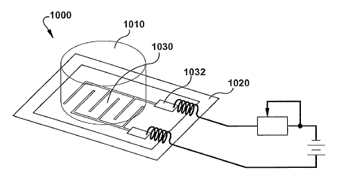
confluence is reached.
[0061] In this example the electric field is generated by an interdigitated
electrode
system 1000 comprising a PLA-coated SPAN film on a nonconductive plastic
substrate
1020. A plastic cylinder 1010 is bonded to the substrate 1020 with a silicone
adhesive
so that the interdigitated electrode 1030 is exposed to the interior volume of
the cylinder
1010, as shown in Figure 10. Thus, the electrode 1030 forms the bottom of a
well, and
CA 02623285 2008-03-20
WO 2007/035849 PCT/US2006/036767
16
the cylinder 1010 forms the sides. The electrode 1030 includes a portion for
forming
electrical contacts 1032, which connect the electrode 1030 to a power supply.
[0062] Before seeding the electrode 1030 with cells the entire well is
sterilized by
washing it twice with phosphate buffered saline, and then irradiating it for
30 minutes
with UV light. Following this treatment, the bottom of the well is evenly
seeded with
trypsinized HOS cells. Additional media is added to the well as needed. The
seeding
density is checked with a hemocytometer and verified to be less than 2 x 10⁴
cells per
well, which is necessary in order to obtain an accurate LSC cell count in the
proliferation
study. The cells are cultured for 24 hours and then, are electrically
stimulated for four
hours using DC power (0-1V) or AC power (10-100KHz, 0-1V). In either case,
electrical stimulation is carried out inside the incubator. Following
stimulation, the cells
are cultured for another 24 hours. The effect of electrical stimulation on
cell growth is
assessed in terms of alkaline phosphatase activity, calcium deposition, and
cellular
proliferation as compared to an appropriate control without electrical
stimulation.
[0063] In this example, alkaline phosphatase activity is determined as
follows.
Twenty microliters of supernatant is collected from each well, mixed with 1 mL
of p-
nitrophenyl phosphate, and incubated at room temperature for about 30 minutes.
The
activity is established by measuring the absorption at 405 nm, which is
directly
proportional to alkaline phosphatase activity.
[0064] In this example, calcium deposition in the extracellular matrix (ECM)
is
measured as follows. The media is removed from each well and I mL of 0.1 N HCI
is
added, which dissolves any calcium that may be present. After incubating at
room
temperature for 2 hours, 20 pL of supernatant is sampled and mixed with 1 mL
of o-
cresolphthalein complex. After five minutes the absorption at 575 nm is
measured, and
the reading is directly proportional to calcium concentration.
[0065] In this example, cellular proliferation is measured as follows. After
the
medium is removed, the cell layer is fixed with 70% ethanol and then stained
with
propidium iodide. Cells can then be observed under fluorescence using laser
scanning
cytometry (LSC) (see Figure 2). Preferably at least five 1.8 mm radius areas
are
randomly sampled and counted. The average number of cells is thus obtained.
CA 02623285 2008-03-20
WO 2007/035849 PCT/US2006/036767
17
Example 2
[0066] In another example of the present invention one or more electrodes are
surgically implanted into an animal. In this example the electrodes comprise
biodegradable and/or bioabsorbable components so that the device need not be
removed from the animal when it is no longer needed. More particularly, the
electrode
of this example comprises biodegradable CPs encased in poly(lactic acid). The
applied
potentia4 can have any appropriate wave form, for example, sinusoidal, square,
triangular or constant. Furthermore, the applied voltage may have any
appropriate
magnitude including 0 to 1600 mV, 50 to 1200 mV, 100 to 1000 mV, and 200 to
800
mV. In some embodiments, the resulting electric field is applied for an amount
of time
effective to influence cellular physiology and/or growth. This is includes
embodiments
where the invention effects only partial healing and/or regeneration.
[0067] The foregoing examples are considered only illustrative of the
principles of
the invention rather than an exclusive list of embodiments. Further, since
numerous
modifications and changes will readily occur to those of ordinary skill in the
art, the
invention is not intended to be limited to the exact construction and
operation shown
and described, and accordingly, all suitable modifications and equivalents are
within the
scope of the present invention.