Note: Descriptions are shown in the official language in which they were submitted.
CA 02623431 2008-03-20
DESCRIPTION
CROSS POLARIZATION INTERFERENCE CANCELING METHOD AND
CROSS POLARIZATION INTERFERENCE CANCELING APPARATUS
Technical Field
[0001] The present invention relates to a technology for canceling
interference between cross polarized waves, in particular, relating to a
preferable cross polarization interference canceling method and cross
polarization interference canceling apparatus that are suitably used for
transmission equipment of a co-channel transmission system in fixed
microwave communications and the like.
Background Art
[0002] As a method for canceling cross polarization interference in
transmission equipment of a co-channel transmission system or the like, an
XPIC (Cross polarization interference Canceller) has been used (see
Japanese Patent Application Laid-open 2000-165339: this publication will be
referred to hereinbelow as patent document 1). This scheme performs
cancellation of cross polarization interference by generating a signal that
cancels the interference signal from an orthogonal polarization wave (which
will be referred to hereinbelow as opposite polarization) relative to an
observable polarization wave (which will be referred to hereinbelow as main
polarization) with reference to the opposite polarization-received signal and
by adding it to the received signal.
[0003] In order to operate the XPIC, it is necessary to synchronize the
interference wave with the carrier component of the main polarization
CA 02623431 2008-03-20
received signal. In a quasi-coherent detection system, the reception local
synchronization scheme for performing synchronization with a local signal on
the receiver side is preferable. In the case of the reception local
synchronization scheme, the local signal on the transmitter side does not
need to be synchronized.
[0004] As a method for realizing reception local synchronization when
using an XPIC in the co-channel transmission system, there are the common
local scheme and the reference synchronization scheme. The common
local scheme braches the output from a single RF local oscillator into two
polarizations and supplies them to receivers for individual polarized waves.
The reference synchronization scheme supplies the output from a
low-frequency reference oscillator to each separate RF local oscillator (LO:
Local Oscillator) in the receiver for each polarization, so that each local
oscillator generates a RF local signal in synchronization with the reference
oscillator to thereby perform synchronization with the local signal for each
polarization.
[0005] Since, in the common local scheme, the output from a single RF
local oscillator is branched into two parts to be supplied to different
polarization receivers, the phase noise of the RF local signal does not affect
the XPIC characteristics. However, if the RF local oscillator breaks down,
the communications through both polarizations shut down, hence it is
disadvantageous in terms of communications path reliability.
[0006] On the other hand, in the reference synchronization scheme,
since each polarization receiver includes its own local oscillator, if one of
them breaks down the transmission path of the other polarization that has not
broken down and that will not shut down. Hence this method is
2
CA 02623431 2008-03-20
advantageous in terms of communications path reliability. However, in this
method, the phase noises from the RF local oscillators cause degradation of
the characteristics of cross polarization interference cancellation. For this
reason, RF local oscillators low in phase noise are used, but such oscillators
low in phase noise are expensive, hence this scheme is disadvantageous in
view of cost.
[0007] A conventional cross polarization interference canceling method
will be described.
[0008] FIG. 1 is a diagram showing a configurational example of a
cochannel transmission system using a common local scheme. IF
(Intermediate Frequency) signals transmitted using V(vertical) - polarization
and H(horizontal) - polarization are converted by means of mixers 1, 1' and
oscillators 2, 2' into RF signals, which are sent out from antennas 3, 3'. The
transmitted signals are received by reception antennas 4, 4' on the receiver
side. Here, for description convenience, pairs of antennas 3, 3' and 4, 4' are
shown separately so as to correspond to individual polarizations. In reality,
however, 3, 3' and 4, 4' are each made of a single antenna.
[0009] In the common local scheme in FIG. 1, the output from single
local oscillator 6 is branched and used as the RF local signals for converting
RF signals into the IF signals.
[0010] FIG. 2 is a diagram showing an interior configurational example of
local oscillator 6. Local oscillator 6 includes reference oscillator 14 that
outputs a low-frequency signal as a reference, phase comparator (PD: Phase
Detector) 15, voltage controlled oscillator 16 and frequency divider 17. Input
to phase comparator 15 are the output from reference oscillator 14 and the
signal that was obtained by frequency-dividing the output from voltage
3
CA 02623431 2008-03-20
controlled oscillator 16 through frequency divider 17. Since the output from
phase comparator 15 is input to voltage controlled oscillator 16, voltage
controlled oscillator 16 constitutes a PLL (Phased Locked Loop) that
oscillates at n-times the frequency of reference local oscillator 14. The
output from voltage controlled oscillator 16 is used as the RF local signal.
[0011] In FIG. 1, the RF signal input to the receiver through antenna 4,4'
is converted to the IF signal through mixer 5,5' and input to orthogonal
demodulator 8,8'. The signal input to orthogonal demodulator 8,8' is
orthogonally demodulated by local oscillator 7,7', then the orthogonally
demodulated signal is input to DEM (demodulator) 9, 9', where the signal is
processed by carrier reproduction, clock reproduction, and the like. The
demodulated result is output as the main signal to adder 10,10'.
[0012] On the other hand, the IF signal input from the opposite
polarization side is also input to orthogonal demodulator 11,11', so that the
orthogonally demodulated signal is input to cross polarization interference
canceller (which will be referred to hereinbelow as XPIC) 12, 12'. In XPIC
12, 12', the opposite polarization signal that has interfered with the main
polarization signal by cross polarization interference arising through the
transmission path is detected to generate and output a signal that cancels it.
The signal output from XPIC 12, 12' is adjusted as to its phase rotation to
that on the main signal side by EPS (Endless Phase Shifter) 13, 13', and the
resultant is added to the main signal at adder 10, 10' to thereby compensate
cross polarization interference.
[0013] FIG. 3 is a circuit block diagram showing in detail one
constructional example of the part downstream of the outputs from
orthogonal demodulators 8 and 11. In FIG. 3, complex multiplier 18, carrier
4
CA 02623431 2008-03-20
phase comparator (Carr PD) 20, loop filter (Carr LPF) 21, accumulator (Acc)
22 and SIN/COS table 23 constitute a carrier reproduction PLL, and this loop
reproduces the carrier.
[0014] In XPIC 24, if there is an opposite polarization input, a signal that
cancels the cross polarization interference component that interfered with the
main polarization is generated. In order to match the carrier phase of the
interference wave mixed in the main polarization with the carrier phase of the
compensating signal output from XPIC 24, complex multiplier 18' rotates the
output signal from XPIC 24 by the same angle as the rotational angle of the
main polarization. The output from complex multiplier 18' is added to the
main polarization at adder 19 so as to cancel cross polarization interference.
Complex multiplier 18' corresponds to a phase rotator.
[0015] Since in the case of this common local scheme, the local signal
used in each polarization receiver is supplied from common local oscillator 6,
the V-polarization that has been affected by phase noise ~ 1, namely signal
V(0 1) and the H-polarization signal that was mixed in due to cross
polarization interference and affected by phase noise 0 1, namely signal
H( 0 1) are input to the V-polarization receiver. Further, as to the opposite
polarization input, the H-polarization signal that has been affected by phase
noise 0 1 is applied in the form of H( 0 1). Here, as to the relationship
between the carrier component of the opposite polarization signal that has
interfered with the main polarization and the carrier component of the
received signal of the opposite polarization signal, they are totally
identical as
to both frequency and phase because the same output from local oscillator 6
is used for processing.
[0016] The phase noise component of the opposite polarization
5
CA 02623431 2008-03-20
component mixed into the main polarization is 0 1 while the phase noise of
the received signal on the opposite polarization side is also 0 1, hence there
is no phase difference between the two signals due to phase noise. XPIC
12 shown in FIG. 1 can generate a phase-stable correcting signal without
having any influence from phase noise when generating a correcting signal.
That is, in this scheme, the phase noise from the local oscillator will not
affect
the capacity of cross polarization interference cancellation.
[0017] However, as stated above the problem entailing the common local
scheme is that communications via both the polarizations shut down all at
once if local oscillator 6 breaks down because the output from this single
local oscillator 6 is branched for use. This feature is disadvantageous in
terms of securing communications path reliability.
[0018] FIG. 4 is a diagram showing a configurational example of a
cochannel transmission system adopting a reference synchronization
scheme. As shown in FIG. 4, this configuration is the same as that of the
common local scheme in FIG. 1 except that each polarization receiver
includes local oscillator 6 or 6'. In the reference synchronization scheme,
each polarization receiver includes local oscillator 6, 6'. Then, in order to
synchronize the frequencies of local oscillators 6, 6' with each other, the
output of a reference signal from low-frequency reference oscillator 25 that
is
to be the reference is branched so that each local oscillator 6, 6' can
generate a local signal synchronized with the reference signal. With this
architecture, if one of local oscillators 6, 6' has broken down, the
transmission path via the other polarization which is not broken will not be
cut
off.
[0019] FIG. 5 is a diagram showing a configurational example of local
6
CA 02623431 2008-03-20
oscillator 6, 6' used in the reference synchronization scheme. As shown in
FIG. 5, local oscillator 6, 6' includes phase comparator 15, voltage
controlled
oscillator 16 and frequency divider 17. Input to phase comparator 15 are a
low-frequency reference signal from without and the signal which is the
output from voltage controlled oscillator 16 that is n-th frequency-divided by
frequency divider 17. Since the output from phase comparator 15 is input to
voltage controlled oscillator 16, voltage controlled oscillator 16 constitutes
a
PLL that oscillates at n-times the frequency of the reference signal input.
The output from voltage controlled oscillator 16 is used as the RF local
signal.
In the reference synchronization scheme, the local signals used for the
polarizations are generated by different PLLs, so that the phase noises
arising have no correlation with the other.
[0020] Accordingly, in the reference synchronization scheme, due to the
phase noises involved with separate local oscillators 6, 6' of the V/H
polarization receivers, the phase relationship between the local signals
output from these local oscillators 6 and 6' is always changing. As a result,
a phase change that reflects the difference between the phase noises of local
oscillators 6 and 6' appears between the phase of the opposite polarization
component that was mixed into the main polarization and the phase of the
received signal on the opposite polarization side. More specifically, as
shown in FIG. 4, when the signal in the V-polarization reception line that was
affected by phase noise 0 1 arising in local oscillator 6 is expressed as V( 0
1), the component from the H-polarization that has interfered with the
V-polarization in the transmission path is affected by phase noise 0 1 that
arises in local oscillator 6, forming H(O 1). Resultantly, a signal V(O
1)+H( 0 1) as the result of cross polarization interference is input to the
7
CA 02623431 2008-03-20
V-polarization reception line.
[0021] On the other hand, in XPIC 12 a H-polarized received signal
named H( 0 2) that has been affected by phase noise 0 2 of local oscillator 6'
from the H-polarization reception line is input. Here, for simplicity the
interference with the H-polarization from the V-polarization will not be
considered. XPIC 12 generates a signal that cancels out H(d) 1) that
interfered with the main polarization input by reference to the opposite
polarization input named H(d)2). At the same time, XPIC 12 has to
generate a correction signal by taking into consideration even the phase
difference (o1- o2). Since an XPIC generally has a phase rotating
function, it is possible to perform correction following the phase difference
1- d) 2) originated from phase noise when the temporal change of this phase
difference is slower than the time constant of the XPIC operation. However,
if phase change exceeding the time constant of the XPIC occurs due to a
phase noise, it is impossible for the XPIC to achieve proper compensation,
then characteristics degradation appears.
[0022] This behavior will be described with FIG. 6. FIG. 6 is a chart
showing the behavior of the phase noise in a RF local signal, representing a
spectrum centered at the oscillation frequency of the local signal. This
shows that the farther away the frequency moves from the center, the lower
the power density becomes, and that the father away the frequency moves
from the center, the smaller the frequency component of the phase noise
becomes. The phase noise component in the limited low-frequency area
can be followed by the XPIC and the influence of the phase noise can be
compensated.
[0023] However, the XPIC cannot react in the region beyond the range
8
CA 02623431 2008-03-20
which is possible for the XPIC to follow the phase noise, so that the phase
noise component is output directly from the XPIC. As a result, when the
XPIC output is added to the main polarization signal, it will not match the
phase of the interference wave in the main polarization, hence producing
compensation error, resulting in characteristic deterioration. It is possible
to
increase the speed for following the phase noise if the time constant of
updating XPIC tap coefficients is made greater. However, this increases the
noise arising from the XPIC itself, so in effect there is a limit to increase
the
time constant of the XPIC. For this reason, when an XPIC based on a
reference synchronization scheme is used, it is necessary to use an
expensive local oscillator that provides low phase noise figure.
Disclosure of Invention
[0024] As described above, when a common local scheme is adopted as
the method of realizing reception local synchronization when an XPIC is used
in the co-channel transmission system, there is the advantage that the phase
noise from the local oscillator will not affect the capacity of cross
polarization
interference cancellation. However, because the output from a single local
oscillator is branched for use, there is the problem that both communications
through the two polarizations shut down all at once if this local oscillator
breaks down. This is disadvantageous in terms of communications path
reliability.
[0025]
On the other hand, the reference synchronization scheme in which the
local oscillator that is provided for each polarization receiver is
frequency-synchronized based on the signal from a reference oscillator has
an advantage that if one local oscillator breaks down, the communication
9
CA 02623431 2008-03-20
path via the other polarization can be secured. However, though either local
oscillator provided for each polarization receiver is frequency-synchronized
based on the signal from the reference oscillator, the phase noise involved in
each local oscillator is irrelevant from the other. Accordingly, there occurs
the problem that the phase noise from each local oscillator causes
characteristic degradation. For improvement against the characteristics
deterioration, a high-cost local oscillator that provides low noise phase
figure
needs to be used.
[0026] In view of the above problems, the object of the present invention
is to provide a cross polarization interference canceling method and
apparatus which can cancel the influence from the phase noise from a local
oscillator having a high level of phase noise and can prevent the phase noise
from deteriorating the cross polarization interference canceling capability
even if an inexpensive oscillator is used.
[0027] A cross polarization interference canceling method of the present
invention is a cross polarization interference canceling method based on a
reception local synchronization scheme for canceling interference between
main polarization and opposite polarization, the method comprises the steps
of: extracting a first phase noise difference that is phase noise difference
between the main polarization and the opposite polarization in the
receiver-side local oscillators, by comparing an error signal that indicates a
difference between a demodulated signal that is the main polarization signal
in which compensation for cross polarization interference has been made
and the received signal which indicates an ideal state of the main
polarization
with a cross polarization interference compensating signal that is the
opposite polarization signal in which compensation for cross polarization
CA 02623431 2008-03-20
interference has been made; and suppressing a second phase noise
difference that is the phase noise difference contained in the cross
polarization interference compensating signal, by using the first phase noise
difference.
[0028] Another cross polarization interference canceling method of the
present invention is a cross polarization interference canceling method based
on a reception local synchronization scheme for canceling interference
between main polarization and opposite polarization, the method comprises
the steps of: extracting a first phase noise difference that is phase noise
difference between the main polarization and the opposite polarization in the
receiver-side local oscillators, by comparing an error signal that indicates a
difference between a demodulated signal that is the main polarization signal
in which compensation for cross polarization interference has been made
and the received signal which indicates an ideal state of the main
polarization
with a cross polarization interference compensating signal that is the
opposite polarization signal in which compensation for cross polarization
interference has been made; and suppressing a second phase noise
difference that is the phase noise difference contained in the opposite
polarization signal based on which the cross polarization interference
compensating signal is generated, by using the first phase noise difference.
[0029] Further, in the above cross polarization interference canceling
method of the present invention, when the vector of the cross polarization
interference compensating signal is a' and the vector of the error signal is e
on the phase rotational angle coordinates, the first phase noise difference 0
may be extracted by
0-2x(La'oe),
11
CA 02623431 2008-03-20
( L a'oe is the angle between vector a' and vector e, inclusive of the
rotational
direction).
[0030] Further, application of the present invention to an XPIC of a
reference synchronization scheme in which in particular, phase noise is
problematic, as a reception local synchronization scheme, is remarkably
preferable in making improvements against characteristics deterioration
arising from the phase noise difference between the receiver side local
oscillators for the main polarization and opposite polarization.
[0031] On the other hand, a cross polarization interference canceling
apparatus of the present invention is a cross polarization interference
canceling apparatus based on a reception local synchronization scheme for
canceling interference between main polarization and opposite polarization,
the apparatus comprises: an error detector for extracting a difference
between a demodulated signal that is the main polarization signal in which
compensation for cross polarization interference has been made and the
received signal which indicates an ideal state of the main polarization and
outputting an error signal that indicates the extracted difference; a phase
noise detector for outputting a phase noise difference by comparing a cross
polarization interference compensating signal that is the opposite
polarization
signal in which compensation for cross polarization interference has been
made with the error signal; a control signal generator for generating a
control
signal corresponding to the phase noise difference; and a phase rotator
disposed prior to, or posterior to, a cross polarization interference
canceller
for generating the cross polarization interference compensating signal, for
controlling the phase of the cross polarization interference compensating
signal in such a direction as to suppress the phase noise difference, in
12
CA 02623431 2008-03-20
response to the input of the control signal.
[0032] In general, a cross polarization interference canceller (XPIC) uses
an adaptively controlled FIR (Finite Impulse Response) filter. In order to
suppress the influence of polarity variation of the control signal due to
noise,
the tap coefficient generator has a relatively large time constant. On the
other hand, the phase rotator, by changing the rotational direction only with
keeping the amplitude unvaried, focuses on the phase rotation as its
controllable parameter, hence a high speed time constant can be expected.
[0033] Further, since usually the influence of phase noise on the local
signal causes a change mainly in phase and brings about little change in
amplitude, controlling the phase by the phase rotator makes it easy to follow
a high-speed phase change caused by the phase noise of the local signal.
[0034] For this reason, according to the present invention, combination
of an XPIC and a phase rotator that is controlled by the signal corresponding
to the phase noise difference between the local signals, provides an
architecture in which the phase noise component is absorbed by the phase
rotator while the other change in amplitude is adjusted by the XPIC itself,
thereby making it possible to suppress influence of phase noise.
[0035] In the present invention, since a means of detecting the difference
between the phase noises in the receiver-side local oscillators for the main
polarization and opposite polarization from the received signal and
suppressing the phase noise difference contained in the cross polarization
interference compensating signal based on the detected result is provided, it
is no longer necessary for the XPIC to follow the phase noise difference.
[0036] Further, since the phase rotator for suppressing phase noise
difference uses a lower number of parameters that are to be varied
13
CA 02623431 2008-03-20
compared to the phase rotation based on a change of the tap coefficients
inside XPIC, the time constant for control can be made small. Accordingly,
it is possible to make the time constant of the XPIC correspondingly greater,
hence it is possible to suppress the noise arising from the XPIC itself when
the time constant of the XPIC is set smaller.
[0037] Also, in an XPIC of a reference synchronization scheme in which
phase noise is problematic, in the present invention, the phase of the
interference component mixed in the main polarization side is adjusted to
phase by detecting the phase noise difference between the local signals by
means of a phase noise detector and giving a phase rotation that will cancel
the phase noise by means of a phase rotator provided at the XPIC output.
Accordingly, even in the reference synchronization scheme, it is possible to
create a condition in which the phase relationship between the carrier
component of the interference wave and the carrier component of the
compensating signal is stable, so that it is possible to prevent degradation
of
the cross polarization interference cancellation characteristics by phase
noise
by following the phase noise of higher frequency components.
[0038] Also, when inexpensive RF local oscillators that present relatively
large phase noise are used to construct an XPIC of a reference
synchronization scheme, it is possible to prevent the lowering of the cross
polarization interference canceling capability based on phase noise.
Brief Description of the Drawings
[0039]
[FIG. 1] FIG. 1 is a diagram showing a configurational example of a
co-channel transmission system adopting a common local scheme.
[FIG. 2] FIG. 2 is a diagram showing a configurational example of the
14
CA 02623431 2008-03-20
inside of a RF local oscillator used for a common local scheme.
[FIG. 3] FIG. 3 is a circuit block diagram showing in detail a constructional
example of the part downstream of the outputs from orthogonal demodulators
in the cross polarization interference canceling apparatus shown in FIG. 1.
[FIG. 4] FIG. 4 is a diagram showing a configurational example of a
co-channel transmission system adopting a reference synchronization
scheme.
[FIG. 5] FIG. 5 is a diagram showing a configurational example of a local
oscillator used in a reference synchronization scheme.
[FIG. 6] FIG. 6 is a chart showing the behavior of phase noise in a RF
local signal.
[FIG. 7] FIG. 7 is a block diagram showing the first exemplary
embodiment of the present invention.
[FIG. 8A] FIG. 8A is a diagram for illustrating the principle of compensating
phase noise in the first exemplary embodiment.
[FIG. 813] FIG. 8B is a diagram for illustrating the principle of compensating
phase noise in the first exemplary embodiment.
[FIG. 8C] FIG. 8C is a diagram for illustrating the principle of compensating
phase noise in the first exemplary embodiment.
[FIG. 9A] FIG. 9A is a diagram for illustrating the principle of compensating
phase noise in the first exemplary embodiment.
[FIG. 9B] FIG. 9B is a diagram for illustrating the principle of compensating
phase noise in the first exemplary embodiment.
[FIG. 10] FIG. 10 is a flow chart for summarizing a cross polarization
interference canceling method in the first exemplary embodiment.
[FIG. 11] FIG. 11 is a block diagram showing the second exemplary
CA 02623431 2008-03-20
embodiment of the present invention.
[Fig. 12] FIG. 12 is a block diagram showing the third exemplary
embodiment of the present invention.
[FIG. 13] FIG. 13 is a flow chart for summarizing a cross polarization
interference canceling method in the third exemplary embodiment.
[Fig. 14] FIG. 14 is an entire block diagram showing the fourth exemplary
embodiment of the present invention.
[FIG. 15] FIG. 15 is a block diagram showing the configuration downstream
of the outputs from orthogonal demodulators in the fourth exemplary
embodiment.
Description of Reference Numerals
[0040]
1,1',5,5' mixer
2,2' oscillator
3,3',4,4' antenna
6,6'7,7' local oscillator
8,8',11,11' orthogonal demodulator
9,9' DEM
10,10',19,29 Adder
12,12',24 cross polarization interference cancelier (XPIC)
13,13' EPS
14,25 reference oscillator
15 phase comparator
16 voltage controlled oscillator
17 frequency divider
18,18' complex multiplier
16
CA 02623431 2008-03-20
20 carrier phase comparator
21 loop filter
22,22' accumulator
23,23' SIN/COS table
26 error detector
27 phase noise detector
28 multiplier
Best Mode for Carrying Out the Invention
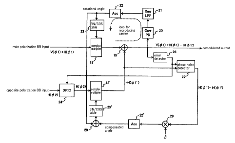
[0041 ] (The first exemplary embodiment)
A cross polarization interference canceling apparatus of the first
exemplary embodiment of the present invention will be described. FIG. 7 is
a block diagram showing an essential part of a cross polarization interference
canceling apparatus of the first exemplary embodiment, in which the portion
downstream of the outputs from orthogonal demodulators 8 and 11 shown in
FIG. 4 is shown. The configuration upstream of orthogonal demodulators 8
and 11 is that shown in FIG. 4. The blocks allotted with the same reference
numerals as in the conventional example shown in FIG. 3 have the same
functions except that input control signals are partly different.
[0042] First, connection for signal transmission between the components
shown in FIG. 7 will be described.
[0043] As shown in FIG. 7, the output side of complex multiplier 18 is
connected to adder 19. Connected to the output side of adder 19 is a signal
line for transmitting demodulated signals. Carrier phase detector (Carr PD)
20 and error detector 26 are connected to this signal line.
[0044] The output side of carrier phase detector 20 is connected to
accumulator 22 via loop filter (Carr LPF) 21. The output signal line from
17
CA 02623431 2008-03-20
accumulator 22 is branched into two, one signal line of the two being
connected to complex multiplier 18 via SIN/COS table 23.
[0045] Input to XPIC 24 is an opposite polarization signal. Complex
multiplier 18' is connected to the output side of XPIC 24. The output signal
line from complex multiplier 18' is branched into two, one signal line of the
two being connected to adder 19.
[0046] The output signal line from error detector 26 is branched into two,
one signal line of the two being connected to phase noise detector 27. The
other signal line is connected XPIC 24. Of the two branched output signal
lines in the above complex multiplier 18', the other signal line is connected
to
phase noise detector 27. The output side of phase noise detector 27 is
connected to adder 29 by way of multiplier 28 and accumulator 22'.
[0047] The other signal line among the two branched output signal line in
the aforementioned accumulator 22 is connected to adder 29. The output
side of adder 29 is connected to complex multiplier 18' via SIN/COS table
23'.
[0048] Next, individual components will be described.
[0049] Complex multiplier 18 corrects the carrier phase of the input main
polarization signal and outputs the signal with its carrier phase
synchronized.
Carrier phase detector 20 detects the phase error of the input demodulated
signal. Loop filter 21 removes high-frequency components from the signal
received from carrier phase detector 29 and outputs the result to accumulator
22. Accumulator 22 generates and outputs a saw-toothed wave having a
frequency corresponding to the magnitude of the signal received from loop
filter 21. SIN/COS table 23 selects a SIN/COS signal that indicates a phase
rotational angle of the saw-toothed wave output from accumulator 22 and
18
CA 02623431 2008-03-20
outputs it to complex multiplier 18.
[0050] XPIC 24 includes a typical adaptively controlled FIR, and when an
opposite polarization signal is input, it generates a signal that cancels the
opposite polarization signal that was mixed into the main polarization by
referring to the signal received from error detector 26. Registered
beforehand in error detector 26 is information that indicates ideal phase
rotational angles for the main polarization signal in complex multiplier 18.
This information is represented, for example by the position of a lattice
point
on the coordinates that show phase rotational angles. Error detector 26
determines the difference between the phase of the received demodulated
signal and the registered ideal phase and outputs the error signal that
indicates the phase difference.
[0051] Phase noise detector 27 determines a phase noise difference to
indicate the phase direction of the phase noise component, based on the
output from complex multiplier 18' and the error determined in error detector
26.
[0052] Multiplier 28 weights the phase noise difference included as a
piece of information in the signal received from phase noise detector 27 in a
predetermined manner, to thereby adjust the control quantity of the phase
noise difference to achieve optimal control of compensation. The signal
including the information on the weighted phase noise difference is output to
accumulator 22'.
[0053] Accumulator 22' reads out the information on the phase noise
difference from the signal received from multiplier 28 and integrates the
phase noise difference and determines a phase compensating angle that
indicates the phase angle to be corrected from the integrated phase noise
19
CA 02623431 2008-03-20
difference and sends it out to adder 29. It is noted that multiplier 28 and
accumulator 22' constitute a control signal generator. The signal output
from the control signal generator corresponds to the control signal of the
present invention.
[0054] When the information on the sum of the phase rotational angle
and the phase compensating angle is input, SIN/COS table 23' selects a
SIN/COS signal that indicates the phase angle corresponding to the
information from the table and sends it out to complex multiplier 18'.
[0055] Complex multiplier 18' corrects the phase angle of the signal in
accordance with the SIN/COS signal received from SIN/COS table 23'. It is
noted that complex multiplier 18' corresponds to the phase rotator of the
present invention.
[0056] Next, signal flow in the cross polarization interference canceling
apparatus of the present exemplary embodiment will be briefly described.
[0057] The carrier phase of the main polarization input signal is corrected
by complex multiplier 18 so that it is output with its carrier synchronized.
The demodulated signal output from adder 19 is input to carrier phase
detector 20, and the phase error is detected by carrier phase detector 20.
High frequency components are removed from the detected phase error
signal by loop filter 21 and the resultant signal is input to accumulator 22.
[0058] Output from accumulator 22 is a saw-toothed wave having a
frequency corresponding to the magnitude of the input signal. This
saw-toothed wave represents the phase rotational angle of the main
polarization signal in complex multiplier 18. Accordingly, a SIN/COS signal
that indicates the phase rotational angle output from accumulator 22 is
selected from the table at SIN/COS table 23, and the SIN/COS signal is input
CA 02623431 2008-03-20
to complex multiplier 18. Here, accumulator 22 and SIN/COS table 23
constitute a numeric controlled oscillator (NCO; Numeric Controlled
Oscillator). The circuitry from phase detector 20 to SIN/COS table 23
constitutes a PLL (Phase Locked Loop) for performing carrier reproduction.
[0059] On the other hand, when an opposite polarization signal is input
into XPIC 24, a signal that cancels the cross-polarized interference wave that
has been mixed into the main polarization is generated in XPIC 24. As the
output from XPIC 24 is input to complex multiplier 18', the signal undergoes
phase correction and is output from complex multiplier 18'. The signal that
was phase corrected at complex multiplier 18' is branched into two, one of
which is added to the main signal at adder 19, the other being input to phase
noise detector 27.
[0060] Error detector 26 determines the error from the lattice point that
indicates the phase of the ideal received signal with regard to the
demodulated signal output from adder 19, and outputs an error signal
indicating that error. Phase noise detector 27 determines a phase noise
difference that indicates the phase direction of the phase noise component,
based on the output from complex multiplier 18' and the error signal
determined at error detector 26. A specific example of determining the
phase noise difference will be described in detail later. Describing the
method briefly, when the output from complex multiplier 18' is expressed as
vector a' and the error signal output of error detector 26 is expressed as
vector e on the phase rotational angle coordinates, phase noise difference
0 from the position (-a) at which vector a' should be originally located can
be determined by 6=7c -2 x( L a'oe).
[0061] The phase difference signal containing the information on the
21
CA 02623431 2008-03-20
determined phase noise difference is input to multiplier 28. Multiplier 28
weights the phase noise difference to be the phase difference of the
determined phase noise with coefficient b, so as to adjust the control
quantity
to achieve optimal control of compensation. The correction control signal
that indicates the adjusted control quantity is integrated at accumulator 22',
and the resultant signal is output as a phase compensating angle that
indicates the phase angle to be corrected.
[0062] When the corrected angle signal containing the information on the
phase compensating angle output from accumulator 22' is input to adder 29,
the phase compensating angle is added to the phase rotational angle on the
main signal side at adder 29, and the resultant signal is input to SIN/COS
table 23'. Then, when the SIN/COS signal obtained from SIN/COS table 23'
is input to complex multiplier 18', the signal input from XPIC 24 is phase
corrected at complex multiplier 18'.
[0063] Next, the operation of the cross polarization interference
canceling apparatus of the present exemplary embodiment will be described.
FIGS. 8 and 9 are diagrams for illustrating the principle of canceling phase
noise in the present exemplary embodiment.
[0064] The loop formed by carrier phase detector 20, loop filter 21,
accumulator 22, SIN/COS table 23 and complex multiplier 18 is a carrier
reproduction PLL. Carrier phase detector 20 outputs the error of the current
carrier phase from an ideal phase. As the output signal is applied to loop
filter 21, loop filter 21 removes high-frequency components from the signal
and coverts it into a frequency signal. When this frequency signal is
determined to be ahead of a phase of the output signal in phase by carrier
phase detector 20, complex multiplier 18 adjusts the phase rotational speed
22
CA 02623431 2008-03-20
in such a direction as to delay the carrier phase (delay frequency). In this
way, carrier synchronization is established.
[0065] XPIC 24, by calculating the correlation between the error signal
from the signal point, detected from the signal that was demodulated from the
main polarization signal by error detector 26 and the opposite polarization
signal input to XPIC 24, detects the opposite polarization signal that had
been mixed in the main signal to thereby generate a signal that compensates
it. The detail of the operation of XPIC 24 is disclosed in patent document 1,
for example, so that a detailed description is omitted herein.
[0066] Error detector 26 detects an error vector to be the vector that
indicates the difference between the actual position of the received signal
and the position (lattice point) at which the main polarization signal is
supposed to be. Phase noise detector 27 determines the phase difference
between the error vector calculated by error detector 26 and the cross
polarization interference signal input from complex multiplier 18' and outputs
an error signal. This error signal is reflective of the phase noise difference
between the main polarization and the opposite polarization.
[0067] As shown in FIG. 9A, XPIC 24 adjusts the amplitude and phase of
the opposite polarization signal that has interfered with the main signal and
outputs the resultant signal. On the other hand, when there is a cause to
generate phase noise, as in the reference synchronization scheme shown in
FIG. 9B, the opposite polarization component mixed in the main signal and
the signal input to the XPIC from the opposite polarization input temporally
change in phase. In this case, XPIC 24 is supposed to correct the phase
change of the phase noise at any time, but the time constant of XPIC is
generally low compared to the frequency characteristics of the phase noise,
23
CA 02623431 2008-03-20
so that the portion in which the phase change of the phase noise cannot be
followed appears as characteristics deterioration.
[0068] As shown in FIG. 8A (shown with an example of QPSK in FIG.
8A), XPIC 24 compensates the interference influence by subtracting the
interference compensating signal generated from the opposite polarization
signal, from the received signal that has undergone cross polarization
interference. In FIG. 8A, for original signal (which indicates an ideal
signal)
D, interference component a is mixed forming the received signal that
deviated from the original shape (four points QPSK). XPIC 24 generates
canceling component a' (=-a) to cancel out this interference component a.
Adding the XPIC output to the received signal that has undergone
interference makes it possible to produce the received signal from which
cross polarization interference has been removed.
[0069] When there is influence of phase noise, the directions of
interference component a and canceling component a' continuously vary
from one moment to another though they are, on average, opposite to each
other. When change in direction is slow, signals that present interference
component a and canceling component a' directed opposite to each other are
generated by the compensating function of XPIC 24, as shown in FIG. 8B.
However, when it exceeds the processing speed of XPIC 24, interference
component a and canceling component a' will not be oriented in exactly the
opposite directions, as shown in FIG. 8C. As a result, error e that cannot be
compensated arises, which finally shifts the received signal point, degrading
the characteristics of the receiver.
[0070] As shown in FIG. 8C, among interference wave a corresponding
to the interference component and compensating signal a' corresponding to
24
CA 02623431 2008-03-20
the canceling component and compensation error e, those which can be
really detected or observed are compensation error e that is the output from
error detector 26 for detecting the error vector between the position(Iattice
point) at which the received signal point is supposed to be and the
demodulation output and compensating signal a' which is the direct output
from complex multiplier 18'. As shown in FIG. 8C, from the relationship
between correction error e and compensation signal a', it is possible to
acquire the knowledge of phase noise difference q between a' and -a.
[0071] That is, when the vector of the cross polarization interference
compensating signal is expressed as a', the vector of the error signal is
expressed as e, and o denotes the reference point of these vectors, phase
noise difference q can be extracted by 0 =n-2 x( L a'oe). Here, Z. a'oe is
the angie formed between vector a' and vector e when vector e is viewed
from vector a' in the counterclockwise direction, as shown in FIG. 8C. If this
phase difference is used to control complex multiplier 18' disposed at the
XPIC 24 output so as to perform phase adjustment in a direction that makes
the phase difference between the phase of the carrier component of the main
polarization and the phase of the carrier component of the cross polarization
interference compensating signal, it is possible to compensate the influence
of the phase noise.
[0072] The correction quantity of the signal output from phase noise
detector 27 is adjusted at multiplier 28 and the signal is converted into a
phase correcting angle at accumulator 22'. Then, the phase correcting
angle from accumulator 22' is added to the phase correcting angle from
accumulator 22 and the resultant signal is output to SIN/COS table 23. The
output from XPIC 24 is phase-rotated by SIN/COS table 23' and complex
CA 02623431 2008-03-20
multiplier 18', so as to achieve control in a direction that reduces the phase
difference between the main polarization signal and the phase noise involved
in the carrier component of the cross polarization interference compensating
signal.
[0073] Since the phase noise has no change in amplitude direction (has
a change in phase only) basically, it is considered that the output signal
from
complex multiplier 18' changes in phase only but not in amplitude while cross
polarization interference in a stable fixed amount is entering. Accordingly,
the tap coefficients in XPIC 24 do not need to follow the phase noise by
performing phase compensation of the phase noise with complex multiplier
18' located at the XPIC 24 output, hence it is possible to prevent the
lowering
of the capability of cross polarization interference cancellation based on the
phase noise.
[0074]
Further, since the phase rotation achieved by complex multiplier 18'
involves a lower number of parameters to be changed compared to phase
rotation by changing tap coefficients in XPIC 24, it is possible to reduce the
time constant for control. Accordingly, the time constant of XPIC 24 is large
correspondingly, hence it is possible to suppress noise arising from the XPIC
itself when the time constant is set low.
[0075] FIG. 10 is a flow chart for summarizing the operational sequence
of the cross polarization interference canceling method in the present
exemplary embodiment. As shown in FIG. 10, error detector 26 determines
the error signal that indicates the difference between the demodulated signal
and the ideal received signal of the main polarization, and phase noise
detector 27 makes comparison between the cross polarization interference
26
CA 02623431 2008-03-20
compensating signal and the error signal, to thereby extract the first phase
noise difference that is the phase noise difference between the main
polarization and opposite polarization in the receiver-side local oscillators
(Step 101). Then complex multiplier 18' suppresses the second phase
noise difference that is the phase noise difference contained in the cross
polarization interference compensating signal, by using the first phase noise
difference (Step 102).
(The second exemplary embodiment)
A cross polarization interference canceling apparatus of the second
exemplary embodiment of the present invention will be described. FIG. 11
is a block diagram showing a cross polarization interference canceling
apparatus of the second exemplary embodiment of the present invention.
The above first exemplary embodiment uses a method of adding the XPIC
signal after establishment of carrier synchronization. The second exemplary
embodiment, however, uses a method of adding the XPIC signal before
establishing carrier synchronization.
[0076] In the present exemplary embodiment, since complex multiplier
18' at the XPIC 24 output needs to simply correct only the phase difference
caused by the influence of the phase noise, the configuration can be
correspondingly simplified. Compared to the first exemplary embodiment,
the configuration for adding the output from accumulator 22 and the output
from accumulator 22' is omitted as shown in FIG. 11.
[0077] Here, the present exemplary embodiment and the first exemplary
embodiment only differ on whether the XPIC signal is added after
establishing carrier synchronization or whether the XPIC signal is added
before establishing carrier synchronization, its basic operation being the
27
CA 02623431 2008-03-20
same as that of the first exemplary embodiment so that description of the
operation is omitted.
[0078](The third exemplary embodiment)
A cross polarization interference canceling apparatus of the third
exemplary embodiment of the present invention will be described. FIG. 12
is a block diagram showing a cross polarization interference canceling
apparatus of the third exemplary embodiment of the present invention. The
present exemplary embodiment has a configuration in which the complex
multiplier 18' in the second exemplary embodiment is disposed on the input
side of XPIC 24. That is, phase compensation can also be performed by
changing the phase of the input signal to XPIC 24. In this case, complex
multiplier 18' is arranged before XPIC 24 as shown in FIG. 12.
[0079] FIG. 13 is a flow chart for summarizing the operational sequence
of the cross polarization interference canceling method in the present
exemplary embodiment. As shown in FIG. 13, error detector 26 determines
the error signal that indicates the difference between the demodulated signal
and the ideal received signal of the main polarization, and phase noise
detector 27 makes comparison between the cross polarization interference
compensating signal and the error signal, to thereby extract the first phase
noise difference that is the phase noise difference between the main
polarization and opposite polarization in the receiver-side local oscillators
(Step 201). Then complex multiplier 18', using the first phase noise
difference, suppresses the second phase noise difference that is the phase
noise difference contained in the opposite polarization signal based on which
the cross polarization interference compensating signal is produced (Step
202).
28
CA 02623431 2008-03-20
[0080](The fourth exemplary embodiment)
A cross polarization interference canceling apparatus of the fourth
exemplary embodiment of the present invention will be described. FIG. 14
is an entire block diagram showing a cross polarization interference
canceling apparatus of the fourth exemplary embodiment of the present
invention. FIG. 15 is a block diagram showing the configuration
downstream of the output from an orthogonal demodulator. FIGS. 14 and
show, respectively, the whole diagram and the configuration downstream
of the outputs from orthogonal demodulators when the present invention is
10 applied to a cross polarization interference canceling apparatus adopting a
coherent detection scheme.
[0081] In the case of a coherence detection scheme, since carrier
synchronization is established at orthogonal detectors 8 and 8', orthogonal
detector 8,8', carrier phase detector 20, loop filter 21 and voltage
controlled
15 oscillator 33 constitute a PLL as shown in FIG . 14. In the case of the
present exemplary embodiment, since carrier synchronization of the input
signals is established, the complex multiplier on the main signal side shown
in FIG. 11 is unnecessary as shown in FIG. 15.
[0082] Also in the present exemplary embodiment, the influence of the
phase noise is removed by complex multiplier 18' arranged at the output of
XPIC 24, in the same manner as in the second exemplary embodiment.
Further, it is also possible to arrange complex multiplier 18' before XPIC 24
as in the third exemplary embodiment described with FIG. 12 though an
example in which complex multiplier 18' is arranged after the output of XPIC
24 in FIG. 15 is explained.
[0083] As described in the first to fourth exemplary embodiments, since
29
CA 02623431 2008-03-20
the present invention includes a means of detecting the difference between
the phase noises in the receiver-side local oscillators for the main
polarization and the opposite polarization from the received signal and
suppressing the phase noise difference contained in the cross polarization
interference compensating signal based on the result, it is not necessary for
the XPIC to follow the phase noise difference.
[0084] Further, since the phase rotator for suppressing phase noise
difference uses a lower number of parameters to be varied compared to the
phase rotation based on a change of the tap coefficients inside XPIC, the
time constant for control can be made small. Accordingly, it is possible to
make the time constant of the XPIC correspondingly greater, hence it is
possible to suppress the noise arising from the XPIC itself when the time
constant of the XPIC is set smaller.
[0085] Also, in the XPIC of a reference synchronization scheme in which
phase noise is problematic, in the present invention, the phase of the
interference component mixed in the main polarization side is adjusted to
phase by detecting the phase noise difference between the local signals by
means of a phase noise detector and giving a phase rotation that will cancel
the phase noise by means of a phase rotator provided at the XPIC output.
Accordingly, even in the reference synchronization scheme, it is possible to
create a condition under which the phase relationship between the carrier
component of the interference wave and the carrier component of the
compensating signal is stable, so that it is possible to prevent degradation
of
the cross polarization interference cancellation characteristics based on
phase noise by following the phase noise of higher frequency components.
[0086] Also, when inexpensive RF local oscillators that present relatively
CA 02623431 2008-03-20
large phase noise are used to construct an XPIC of reference
synchronization scheme, it is possible to prevent the lowering of the cross
polarization interference canceling capability based on phase noise.
[0087] The present invention should not be limited to the above
exemplary embodiments, but various modifications can be made within the
scope of the present invention and those of course should be included in the
scope of the invention.
31