Note: Descriptions are shown in the official language in which they were submitted.
CA 02624014 2008-03-27
~~~~~~1-C A I ION
SEMICONDUCTOR OPTICAL ELEMENT AND EXTERNAL CAVITY LASER
HAVING THE SEMICONDUCTOR OPTICAL ELEMENT
Technical Field of the Invention
[00011
The present invention relates to a semiconductor optical element and an
external
cavity laser having the semiconductor optical element.
Background of the Invention
[0002]
Up until now, there have been proposed a wide variety of semiconductor optical
elements of this type, one typical example of which needs to include a
waveguide having
one end surface with low reflectivity and one end surface with high
reflectivity. Each of
the semiconductor optical elements is to be applied to an optical device such
as an external
cavity laser diode (EC-LD) and a superluminescent diode (SLD).
[0003]
To reduce the reflectivity of the end surface of the waveguide, the following
waveguides have been proposed: a waveguide having a window structure at the
end surface
thereof; and a waveguide including an end portion having an optical axis,
which is not
perpendicular to the end surface thereof.
[0004]
The waveguide provided with the window structure, however, may have a crystal
defect in the vicinity of the window structure. The occurrence of the crystal
defect may
reduce reliability of a semiconductor optical element having the waveguide.
[0005]
To avoid the above problem, there has been proposed a semiconductor optical
element including a waveguide having an optical axis, which is not
perpendicular to an end
surface of the semiconductor optical element (refer to, for example, Patent
Documents 1 and
2).
[0006]
FIG 13(a) is a top view of a semiconductor optical amplifier (SOA) 110, which
is
one of semiconductor elements disclosed in Patent Document 1. The
semiconductor
optical amplifier 110 includes a linear waveguide 110G having an optical
axis,, which is not
perpendicular to a cleavage surface 110G1 and a cleavage surface 110G2 of the
1
CA 02624014 2008-03-27
semiconductor optical amplifier 110. Patent Document 1 also discloses that
reflectivity of
a traveling-wave laser amplifier is reduced by flaring a waveguiding portion
of the amplifier
in the immediate vicinities of the end surfaces of the waveguide 110G.
[0007]
FIG. 13(b) is a top view of an optical device 130 having an EC-LD 120, which
is
one of semiconductor elements disclosed in Patent Document 2. The EC-LD 120
has
cleavage surfaces 120G1 and 120G2 and includes a waveguide 120G having an end
surface
low reflectivity and an end surface with high reflectivity. The low-
reflectivity end surface
of the waveguide 120G is inclined at a predetermined angle with respect to the
cleavage
surface 120G1, while the high-reflectivity end surface of the waveguide 120G
is
perpendicular to the cleavage surface 120G2.
[0008]
In the optical device 130, light is generated in the waveguide 120G, reflected
on
the high-reflectivity end surface of the waveguide 120G, and returned to the
inside of the
waveguide 120G. The light then reaches a diffraction grating 122 through a
collimator
lens 121.
[0009]
Among the light diffracted by the diffraction grating 122, only light having a
wavelength satisfying a predetermined condition is reflected on a recursive
mirror 123,
diffracted by the diffraction grating 122 again, and returned to the EC-LD
120. The optical
device 130 is designed to select a frequency of laser oscillation. The light
is output from
the optical device 130 to the side opposite to the EC-LD 120 through
diffraction on the face
of the diffraction grating 122.
Patent Document 1: U.S. Pat. No. 4965525 (pages 2 to 5, FIG 1)
Patent Document 2: U.S. Pat. No. 6091755 (page 5, FIG. 2)
Disclosure of the Invention
Problems to be solved by the Invention
[0010]
The conventional semiconductor element disclosed in Patent Doctunent 1 is
designed for a semiconductor optical amplifier (SOA) having a waveguide with
low-reflectivity end surfaces. The semiconductor element disclosed in Patent
I)ocument 1
cannot be thus applied to an EC-LD, which requires certain reflectivity at one
end surface
thereof.
[00111
2
CA 02624014 2008-03-27
The conventional semiconductor element disclosed in Patent Document 2 includes
a waveguide having an end surface with low reflectivity and another end
surface with high
reflectivity, the end surface with low reflectivity being not perpendicular to
a cleavage
surface of the EC-LD, the end surface with high reflectivity being
perpendicular to a normal
to another cleavage surface of the EC-LD. The semiconductor element disclosed
in Patent
Document 2 can be applied to an EC-LD and SLD. The end surface with high
reflectivity
has reflectivity of 30 % or more without being coated. This reflectivity is
excessively high
for the semiconductor element disclosed in Patent Document 2, which is to be
applied to an
EC-LD or SLD. As described above, it is necessary that the light be output
from the side
of the diffraction grating, or that the end surface of the waveguide be coated
by an
antireflection film to reduce the reflectivity, which prevents a large amount
of light from
being output, or which makes the manufacturing process complicated.
[0012]
The conventional semiconductor optical element disclosed in Patent I)ocument 2
includes a waveguide having an end surface inclined with respect to the
surface of the laser
and another end surface perpendicular to a normal to the other surface of the
laser. This
makes it difficult to downsize an optical device having the conventional
semiconductor
optical element, or makes the assembly of the optical device complicated.
[0013]
It is, therefore, an object of the present invention to provide a
semiconductor
optical element applicable to an EC-LD or an SLD, and an external cavity laser
having the
semiconductor optical element, which has an end surface with low reflectivity
and another
end surface with certain reflectivity and includes a waveguide, each of the
end surfaces
being not perpendicular to an optical axis of a corresponding one of end
portions of the
waveguide.
Means for Solving the Invention
[0014]
The semiconductor optical element according to an aspect of the present
invention
has a pair of cleavage surfaces, and comprises: a semiconductor substrate
having a base
surface; and a planer structure provided on the base surface and provided with
a waveguide
having an active layer; wherein the waveguide has first and second end
surfaces defined by
the respective cleavage surfaces, the first end surface of the waveguide has
first reflectivity,
the second end surface has second reflectivity, the waveguide includes one end
portion
having an optical axis being at a first angle to a normal to the first end
surface, and one end
portion having an optical axis being at a second angle to a normal to the
second end surface,
3
CA 02624014 2008-03-27
the waveguide guides light so that the light is output from the first end
surface in a first
direction, and that the light is output from the second end surface in a
second direction
parallel to the first direction, and the light guided by the waveguide in the
vicinity of the
first end surface has a first spot size measured in a lateral direction of the
waveguide, and
the light guided by the waveguide in the vicinity of the second end surface
has a second spot
size measured in the lateral direction of the waveguide, the first spot size
being different
from the second spot size.
[0015]
In the semiconductor optical element thus constructed, the direction of
propagation
of the light output from the first end surface is parallel to that of
propagation of the light
output from the second end surface under the condition that the first
reflectivity is different
from the second reflectivity.
[0016]
The semiconductor optical element according to another aspect of the present
invention having a pair of cleavage surfaces parallel to each other, and
comprises: a
semiconductor substrate having a base surface; and a planar structure provided
on the base
surface and provided with a waveguide having an active layer, wherein the
waveguide has
first and second surfaces defined by the respective cleavage surfaces, the
waveguide
includes one end portion having an optical axis being at a first angle to a
normal to the first
end surface, and one end portion having an optical axis being at a second
angle to a normal
to the second end surface, the first angle being not equal to zero, the second
angle being not
equal to zero and different from the first angle, the waveguide guides light
so that the light is
output from the first end surface in a first direction, and that the light is
output from the
second end surface in a second direction parallel to the first direction, and
the light guided
by the waveguide in the vicinity of the first end surface has a first spot
size measured in a
lateral direction of the waveguide, and the light guided by the waveguide in
the vicinity of
the second end surface has a second spot size measured in the lateral
direction of the
waveguide, the first spot size being different from the second spot size.
[0017]
In the semiconductor optical element thus constructed, the direction of
propagation
of the light output from the first end surface is parallel to that of
propagation of the light
output from the second end surface under the condition that the first
reflectivity is different
from the second reflectivity.
[0018]
The semiconductor optical element according to still another aspect of the
present
invention having a pair of cleavage surfaces, and comprises a semiconductor
substrate
4
CA 02624014 2008-03-27
having a base surface; and a planer structure provided on the base surface and
provided with
a waveguide having an active layer, wherein the waveguide has first and second
end
surfaces defined by the respective cleavage surfaces, the waveguide includes
one end
portion having an optical axis being at a first angle to a normal to the first
end surface, and
one end portion having an optical axis being at a second angle to a normal to
the second end
surface, the first angle being not equal to zero, the second angle being not
equal to zero and
different from the first angle, the waveguide guides light so that the light
in the vicinity of
the first end surface has a first spot size measured in a lateral direction of
the waveguide,
and the light in the vicinity of the second end surface has a second spot size
measured in the
lateral direction of the waveguide, the first spot size being different from
the second spot
size.
[0019]
In the semiconductor optical element thus constructed, the first end surface
has
reflectivity different from that of the second end surface.
[0020]
The semiconductor optical element according to still another aspect of the
present
invention may comprise a waveguide having a first width at the first end
surface and a
second width at the second end surface, the first width being larger than the
secorid width.
[00211
The semiconductor optical element according to still another aspect of the
present
invention comprises a waveguide having first and second linear portions, the
first linear
portion having a first width and extending a predetermined distance from the
first end
surface, the second portion having a second width and extending a
predetermined distance
from the second end surface.
[0022]
The semiconductor optical element thus constructed is capable of preventing a
variation in the angle of the optical axis of each of the end portion of the
waveguide with
respect to the normal to a corresponding one of the first and second end
surfaces of the
waveguide, and a variation in the reflectivity of each of the end surfaces of
the waveguide
even if either one of or both the first and second end surfaces of the
waveguide is or are
misaligned from a desired position(s) on the corresponding cleavage
surface(s).
[0023]
The external cavity laser according to the present invention comprises a
semiconductor optical element as set forth in any one of claims 1 to 5, and
liglit feedback
means for causing light having a specified wavelength, which is output from
the first end
surface of the waveguide, to selectively return to the first end surface among
light output
5
CA 02624014 2008-03-27
from the first end surface of the waveguide, the light having the specified
wavelength being
output from the second end surface of the waveguide.
[0024]
The external cavity laser thus constructed allows an optical system to be
simply
designed and easily assembled, and allows the optical device to be downsized
and a large
amount of light to be output.
[0025]
The present invention provides a semiconductor optical element applicable to
an
EC-LD or an SLD, and an external cavity laser having the semiconductor optical
element
provided with the waveguide, which has an end surface with low reflectivity
and another
end surface with certain reflectivity, each of the end surfaces being not
perpendicular to an
optical axis of a corresponding one of the end portions of the waveguide.
Brief Description of the Drawings
[0026]
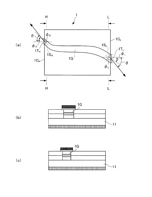
FIG 1(a) is a top view of a semiconductor optical element according to the
first
embodiment of the present invention.
FIGs. 1(b) and 1(c) are each a cross-sectional view of the semiconductor
optical
element according to the first embodiment.
FIG 2 is a graph showing the relationship between reflectivity R and an angle
~ of
an optical axis of an end portion of the waveguide in the vicinity of an end
surface of the
waveguide with respect to a normal to an end surface of the waveguide.
FIG 3 is a graph showing the relationship (indicated by a solid line) between
a spot
size co of light and the width W of the waveguide, the relationship (indicated
by a dashed
line) among the width W of the waveguide, an angle ~ of the optical axis of
the end portion
of the waveguide in the vicinity of the end surface of the waveguide with
respect to the end
surface of the waveguide, and an angle 0 of the direction of propagation of
light to be output
with respect to the end surface of the waveguide.
FIG 4 is a diagram showing an example of a process of manufacturing the
semiconductor optical element according to the first embodiment.
FIG 5 is a diagram showing the example of the process of manufacturing the
semiconductor optical element according to the first embodiment.
FIGs. 6(a) and 6(b) are enlarged views respectively showing the vicinity of a
first
end surface 1TL and the vicinity of a second end surface 1TH of the waveguide.
FIG. 7 is a top view of an external cavity laser using the semiconductor
optical
element according to the first embodiment.
6
CA 02624014 2008-03-27
FIG 8 is a block diagram showing an external cavity laser that employs a
Littman
design.
FIG 9 is a block diagram showing an external cavity laser using an etalon.
FIG 10 is a block diagram showing an external cavity laser using an
acousto-optical modulator (AOM).
FIG 11 is a block diagram showing an external cavity laser using a ring
resonator.
FIG 12 is a block diagram showing an external cavity laser using an FBG.
FIG 13(a) is a top view of a conventional semiconductor optical element.
FIG 13(b) is a top view of a conventional optical device having a
semiconductor
optical element.
Description of Reference Numerals
[0027]
1: Semiconductor optical element
1 G: Waveguide
1TL: First end surface
1TH: Second end surface
4: Light feedback means
5: Light output means
11: Semiconductor substrate
13: Active layer
100: External cavity laser
Best Mode for Carrying Out the Invention
[0028]
Embodiments of the semiconductor optical element and the external cavity laser
having the semiconductor optical element according to the present invention
are described
below with reference to the accompanying drawings.
[0029]
(First Embodiment)
FIG 1(a) is a top view of a semiconductor optical element 1 according to the
first
embodiment of the present invention. FIGs. 1(b) and 1(c) are each a cross-
sectional view
of the semiconductor optical element 1 according to the first embodiment.
[0030]
As shown in FIG. 1(a), the semiconductor optical element 1 having a pair of
cleavage surfaces, and comprises a semiconductor substrate 11 having a base
surface, and a
7
CA 02624014 2008-03-27
planer structure provided on the base surface and provided with a waveguide 1G
having an
active layer, wherein the waveguide 1G has a first end surface 1TL and a
second end surface
1TH which are defined by the cleavage surfaces.
[0031]
The waveguide includes an opening having a surface defined as the first end
surface 1TL in a first cleavage surface 1CL of the semiconductor optical
element 1 and an
opening having a surface defined as the second end surface 1TH in a second
cleavage
surface 1CH of the semiconductor optical element 1.
[0032]
The waveguide 1G includes an end portion having an optical axis in the
vicinity of
the first end surface 1TL and another end portion having another optical axis
in the vicinity
of the second end surface 1TH. The optical axis in the vicinity of the first
end surface 1TL
and a normal to the first end surface 1TL form a first angle ~L which is not
zero degree,
while the optical axis in the vicinity of the second end surface 1TH and a
normal to the
second end surface 1TH form a second angle ~H which is not zero degree and is
different
from the first angle ~L.
[0033]
The waveguide 1G is adapted to guide light. The light guided by the waveguide
1G in the vicinity of the first end surface 1TL has a first spot size measured
in a lateral
direction of the waveguide, while the light guided by the waveguide 1G in the
vicinity of
the second end surface 1TH has a second spot size measured in the lateral
direction of the
waveguide, the first and second spot sizes being different from each other.
[0034]
The direction of propagation of light output from the first end surface 1TL of
the
waveguide 1G is parallel to the direction of propagation of light output from
the second end
surface 1Tn of the waveguide 1G.
[0035]
The waveguide has a first waveguide cross section 1SL and a second waveguide
cross section 1SH. The first waveguide cross section 1SL is taken along a line
extending
between a point located on the first end surface 1TL of the waveguide and on a
first side
surface of the waveguide and a point located on a second side surface of the
waveguide and
on a normal to the first side surface of the waveguide. The first end surface
1TH of the
waveguide is at first angle ~L to the first waveguide cross section 1 SL. The
second
waveguide cross section 1SH is taken along a line extending between a point
located on the
second end surface 1TH of the waveguide and on the second side surface of the
waveguide
and a point located on the first side surface of the waveguide and on a normal
to the second
8
CA 02624014 2008-03-27
side surface of the waveguide. The second end surface 1TL of the waveguide is
at the
second angle ~H to the second waveguide cross section 1SL.
[0036]
As shown in FIG. 1(b) illustrating a cross sectional view taken along line L-L
of
FIG 1(a) and FIG 1(c) illustrating a cross sectional view taken along line H-H
of FIG 1(a),
the area of the first waveguide cross section 1SL is larger than that of the
second waveguide
cross section 1SH. The first end surface 1TL has first reflectivity RL, and
the second end
surface 1TH has second reflectivity RH. The first reflectivity RL is smaller
than the second
reflectivity RH. The height of the waveguide 1G is constaint in general, the
height being
defined as a distance measured in a direction perpendicular to the base
surface of the
semiconductor substrate. The width of the waveguide 1G in the first waveguide
cross
section 1SL is larger than the width of the waveguide 1G in the second
waveguide cross
section 1SH, the widths being defined as distances measured in the lateral
direction of the
waveguide.
[0037]
The first reflectivity RL of the first end surface 1TL defined by the first
cleavage
surface 1CL needs to be approximately 0.01 % so that the semiconductor optical
element
according to the first embodiment can be applied to an EC-LD or SLD. Coating
an
antireflection film can reduce the reflectivity to 1/1000 of the reflectivity.
The first
reflectivity RL of the first end surface 1TL, which is not coated with the
antireflection film,
is preferably about a tenth of reflectivity of the first end surface 1TL
obtained in the case
where the first end surface 1TL is perpendicular to the first cleavage surface
1CL and an
antireflection film is not provided.
[0038]
FIG 2 is a graph showing the relationship (Equation 1) between the
reflectivity R
and the angle ~(~a <4 <k <~a) of the optical axis of the end portion of the
waveguide
with respect to the normal to the end surface of the waveguide. The spot size
0) (wa < wb <
(oc < wa) of the light propagating in the waveguide 1G is used as a parameter.
(Equation 1)
R = h(~,(o)
Equation 1 depends on the structure of the semiconductor optical element, and
the
detail of Equation 1 is thus not described. Details of the following Equations
2 and 3 are
not described for the same reason.
[0039]
As apparent from the graph shown in FIG. 2, when the first reflectivity RL of
the
first end surface 1TL is set to 10 %, and a spot size COd is selected as the
spot size wL, the
9
CA 02624014 2008-03-27
angle ~L of the optical axis of the waveguide 1G on the side of the first end
surface 1TL
with respect to the normal to the first end surface 1TL is the angle ~a.
[0040]
FIG. 3 is a graph showing the relationship (indicated by a solid line) between
the
spot size w of light and the width W of the waveguide, and the relationship
(indicated by a
dashed line) among the width W of the waveguide, the angle ~ of the optical
axis of the
waveguide in the vicinity of the end surface of the waveguide with respect to
the normal to
the end surface of the waveguide, and the angle 0 of the direction of
propagation of light to
be output with respect to the normal to the end surface of the waveguide. The
relationship
between the spot size w of light and the width W of the waveguide is expressed
by Equation
2.
(Equation 2)
co = f(W)
[0041]
The relationship between the width W of the waveguide and a refractive index n
in
the vicinity of the end surface of the waveguide is expressed by Equation 3.
(Equation 3)
n = g(W)
[0042]
Among the refractive index obtained by Equation 3, the angle 0 of the
direction of
propagation of light to be output with respect to the normal to the end
surface of the
waveguide, and the angle ~ of the optical axis of the waveguide in the
vicinity of the end
surface of the waveguide with respect to the normal to the end surface of the
waveguide,
Snell's law is applied. Thus, Equation 4 is expressed by use of the angle ~,
the angle 0,
and the width W of the waveguide.
(Equation 4)
sinO = n/no sino = g(W)sino
where no is a refractive index of air = 1
[0043]
Each of the dashed lines shown in FIG. 3 indicates the relationship (Snell's
law
under the condition that the angle 0 is constant) between the width W of the
waveguide and
the angle 0 of the direction of propagation of light to be output with respect
to the normal to
the end surface of the waveguide under the condition that the angle 0 (01 <02
<: 3 <04) is
constant.
[0044]
The angle 9L of the direction of propagation of light to be output from the
first end
CA 02624014 2008-03-27
surface 1TL with respect to the normal to the first end surface 1TL of the
waveguide is
determined in accordance with a specification of the semiconductor optical
element and
with a specification of a semiconductor module having the semiconductor
optical element
therein. For example, if the angle OL needs to be 20 degrees, Equation 5 is
expressed.
(Equation 5)
nLsin~L = sin20 = 0.342
[0045]
The angle ~L and the width WL of the waveguide in the first waveguide cross
section 1SL are determined by procedures described below, the angle ~L being
formed
between the optical axis of the end portion of the waveguide in the vicinity
of the end
surface of the waveguide and the normal to the first end surface of the
waveguide.
[0046]
(1) The first reflectivity RL (e.g., 10 %) and the angle OL (e.g., 20 degrees)
are set.
[0047]
(2) According to Equation 4 (dashed lines shown in FIG. 3), a candidate value
(~Z <_
~<_ ~4) of the angle +L that can be obtained based on the angle 8L is
tentatively set.
[0048]
(3) According to Equation 4 (dashed lines shown in FIG 3), the width W(W1 S W
W3) of the waveguide is obtained so that the angle 0 is OL and the angle + is
equal to or
smaller than +Z and equal to or larger than+4. The width W(e.g., WZ S W<_':
W3) of the
waveguide is preferably within a range, in which a variation in the spot size
w of light is
smaller than a variation in the width W of the waveguide in the process for
manufacturing
the semiconductor optical element, as a candidate of the width WL of the
waveguide.
[0049]
(4) According to Equation 3 (solid lines shown in FIG 2), the spot size (D
(c), <o) <
w2) is obtained for each of candidates of the width WL of the waveguide. A
combination
of a candidate of the angle 4 and a candidate of the first spot size wL is
determined.
[0050]
(5) According to Equation 1(FIG 2), a combination of the angle +L and the
first
spot size OL, which leads to the reflectivity RL of 10 %, is selected among
combinations of
the candidates, to determine the width WL of the waveguide corresponding to
the selected
combination.
[0051]
When the width WL (3.5 to 4.5 m) of the waveguide, which leads to the fact
that
the refractive index of the first end surface 1TL is 3.2, is selected, the
angle +L is 6.1
degrees.
11
CA 02624014 2008-03-27
[00521
Next, the angle ~H and the width WH of the waveguide in the second waveguide
cross section 1SH are determined by procedures described below, the angle ~H
being formed
between the optical axis of the waveguide in the vicinity of the second end
surface 1TH of
the waveguide and the normal to the second end surface 1TH of the waveguide.
[0053]
The reflectivity of the second end surface 1TH of the waveguide needs to be
high.
As shown in FIG 2, however, the higher the reflectivity of the second end
surface 1TH is,
the smaller the spot size w(O)a < (Ob < wc < cOa) is, under the condition that
the angle + is
constant. If the second spot size wH of light at the second end surface 1TH is
set as small
as possible, high reflectivity of the second end surface 1TH can be obtained.
100541
When the width WL (e.g., W2 <_ W<_ W3) of the waveguide is within a range in
which the variation in the spot size co is smaller than the variation in the
width W of the
waveguide in the process for manufacturing the semiconductor optical element,
the width
WH of the waveguide at the second end surface 1TH is smaller than the width WL
of the
waveguide at the first end surface 1TL.
[0055]
The spot size w indicates a curved line protruding downward and is a function
of
the width W of the waveguide, as expressed by Equation 2 (solid line shown in
FIG 3).
The spot size w shows the minimum value when the width of the waveguide is Wo.
[0056]
When the minimum value of the spot size w is w, the angle +H needs to be
larger
than the angle +a and smaller than the angle +b based on the graph shown in
FICi 2 in order
to ensure the reflectivity of about 20 % on the side of the second end surface
1TH.
[0057]
When the angle 6H of the direction of propagation of light output from the
second
end surface 1TH with respect to the normal to the second end surface 1TH of
the waveguide
is 20 degrees which is the same as the angle 6L of the direction of
propagation of light
output from the first end surface 1TL with respect to the normal to the first
end surface 1TL
of the waveguide, the product of the sine of the angle +H and the refractive
index n of the
second end surface 1TH needs to satisfy Equation 6.
(Equation 6)
nHsin~H = sin20 = 0.342
[0058]
Since the refractive index nH is determined as a function of the width WH of
the
12
CA 02624014 2008-03-27
waveguide by using Equation 2, the angle ~H is determined.
[0059]
If the refractive index nH is 3.3 when the width WH of the waveguide is 1.8
m, the
angle ~H is 6.0 degrees and the reflectivity is 20 %, which makes it possible
to achieve the
semiconductor optical element.
[0060]
Next, the process for manufacturing the semiconductor optical element 1 will
be
described as an example with reference to FIGs. 4 and 5.
[0061]
First step: Using a metal organic vapor phase epitaxy (MOVPE) method, an n-
type
InP cladding layer 12, an InGaAsP active layer 13 having a multiple quantum
well structure,
a first p-type InP cladding layer 14, and a p-type InGaAsP cap layer 15 are
sequentially
laminated on a n-type InP semiconductor substrate.
[0062]
Second step: Using a chemical vapor deposition (CVD) method, an SiNx layer 16
is formed on the cap layer 15.
[0063]
Third step: Using a photolithography method, a mask pattern is transferred to
the
SiNx layer 16.
[0064]
Fourth step: Using wet etching or dry etching, a mesa structure is formed,
which
includes the n-type InP cladding layer 12, the active layer 13, the first p-
type InP cladding
layer 14, the cap layer 15, and the SiNx layer 16 used as an etching mask.
[0065]
Fifth step: Using the MOVPE method, a p-type InP lower buried layer 17 and an
n-type upper buried layer 18 are sequentially laminated on both sides of the
mesa structure
with the SiNx layer 16 used as a growth prevention mask.
[0066]
Sixth step: The SiNx layer 16 is removed by using a hydrofluoric acid, and the
cap
layer 15 is removed by using a sulfuric acid and an aqueous hydrogen peroxide
solution.
[0067]
Seventh step: Using the MOVPE method, a second p-type InP cladding layer 19
and a p-type InGaAs contact layer 20 are sequentially laminated on the first p-
type InP
cladding layer 14 and the n-type upper buried layer 18.
[0068]
Eighth step: a p-type metal electrode l0a is formed on the contact layer 20,
and an
13
CA 02624014 2008-03-27
n-type metal electrode lOb is formed under the semiconductor substrate 11, to
complete a
wafer.
[0069]
Ninth step: the wafer is cut along a predetermined line (X1Xl', X2X2', X3X3',
etc.)
so that cleavage surfaces of the semiconductor optical element are parallel to
each other and
that multiple elements are arranged side-by-side and each of the multiple
elements forms a
bar.
[0070]
Tenth step: An antireflection film 101 is coated on the side of a low-
reflectivity end
surface.
[00711
Eleventh step: The bar is cut along a predetermined line (YIYI', Y2Y2', Y3Y3',
Y4Y4', etc.) for each of the semiconductor optical elements.
[0072]
As shown in the enlarged views of FIG. 6 illustrating the first end surface
1TL and
the second end surface iTH, the waveguide 1G preferably includes a first
linear potion
having a first width 1DL and extending a predetermined distance from the first
end surface
1TL and a second linear portion having a second width 1DH and extending a
predetermined
distance from the second end surface 1TH.
[0073]
In the present embodiment, the width of the waveguide is gradually increased
from
the second linear portion to the first linear portion, and the waveguide has a
connecting
portion, which connects the first and second linear portions and is smoothly
curved. The
waveguide in the present embodiment, however, is not limited to the waveguide
having the
abovementioned shape.
[0074]
The waveguide 1G has the linear portions on both end sides in order to prevent
a
variation in the angle 0 of the optical axis of the each of the linear
portions with respect to
the normal to each of the first and second end surfaces and a variation in the
reflectivity
even if either one of or both the first end surface and the second end surface
is or are
misaligned from a desired position(s) on either one of or both the first
cleavage surface 1CL
and the cleavage surface 1CH.
[0075]
FIG. 7 is a top view of an external cavity laser 100 using the semiconductor
optical
element 1 according to the first embodiment. The external cavity laser 100
includes a
reflecting mirror 21 (e.g., a liquid crystal tunable mirror) having wavelength
selectivity,
14
CA 02624014 2008-03-27
which is arranged on the direction of propagation of light output from the
first end surface
1TL of the waveguide 1G. The external cavity laser 100 also includes a
collimate lens 22
and an optical fiber connection terminal 23, which are arranged on the
direction of
propagation of light output from the second end surface 1TH of the waveguide
1G.
[0076]
The optical axis XL passing through the reflecting mirror 21 can be parallel
to the
optical axis LH passing through the collimate lens 22 and the optical fiber
connection
terminal 23, since the angle 6L of the direction of propagation of light
output from the first
end surface 1TL with respect to the first end surface 1TL of the waveguide 1G
is an angle 0,
which is the same as the angle 9H of the direction of propagation of light
output from the
second end surface 1TH with respect to the second end surface 1TH of the
waveguide 1G.
[0077]
The external cavity laser 100 using the semiconductor optical element 1
according
to the first embodiment functions as an EC-LD. Light generated in the
semiconductor
optical element 1 passes through the first end surface 1TL having low
reflectivity, is
reflected by the reflecting mirror 21 having wavelength selectivity, and
returns to the
semiconductor optical element 1. Part of the light returned to the
semiconductor optical
element 1 is reflected by the second end surface 1TH having high reflectivity,
while the
other part of the light is output from the second end surface 1TH to an
optical fiber through
the collimate lens 22 and the optical fiber connection terminal 23.
[0078]
As described above, the waveguide of the semiconductor optical element
according
to the first embodiment has a low-reflectivity end surface and a high-
reflectivity end surface.
The angle of the direction of propagation of light output from the low-
reflectivity end
surface of the waveguide with respect to the low-reflectivity end surface of
the waveguide is
the same as the angle of the direction of propagation light output from the
high-reflectivity
end surface of the waveguide with respect to the high-reflectivity of the
waveguide even if
the optical axis of the waveguide in the vicinity of one of the end surfaces
of the waveguide
is not perpendicular to the one of the end surfaces of the waveguide.
[0079]
In the present embodiment, the directions of propagation of light output from
both
end surfaces of the waveguide are parallel to each other. The structure of the
waveguide,
however, is not limited to the above. The semiconductor optical element allows
:light output
from each end surface to propagate in a desired direction to meet a
specification of a
semiconductor module having the semiconductor optical element therein.
[0080]
CA 02624014 2008-03-27
(Second Embodiment)
The external cavity laser using the semiconductor optical element will be
described,
which is an optical device.
[0081]
As shown in FIG. 8, the external cavity laser according to the present
invention is
provided with the semiconductor optical element 1 according to the first
embodiment, light
feedback means 4 for causing light having a specified wavelength output from
the first end
surface 1TL of the waveguide 1G to selectively return to the first end surface
1TL; and light
output means 5 for outputting light having a specified wavelength from the
second end
surface 1TH of the waveguide 1G.
[0082]
The light feedback means 4 includes a collimate lens 41, a diffraction grating
42, a
recursive reflecting mirror 43, and an actuator (not shown). The light output
means 5
includes a collimate lens 51 and an optical fiber 52.
[0083]
FIG. 8 is a block diagram showing the external cavity laser that employs a
Littman
design.
[0084]
In the external cavity laser, part of light reached to the second end surface
ITH of
the waveguide 1G is reflected by the second end surface 1TH having high
reflectivity, while
the other part of the light is output from the second end surface 1TH to the
optical fiber 52
through the collimate lens 51.
[0085]
The light output from the first end surface ITL of the wadveguide 1G is
collimated
by the collimate lens 41 and diffracted by the diffraction grating 42. The
diffracted light is
reflected by the recursive reflecting mirror 43 and returns to the
semiconductor optical
element 1 through the diffraction grating 42.
[0086]
The recursive reflecting mirror 43 is rotatable about a rotation center 44
thereof by
use of an actuator (not shown). The recursive reflecting mirror 43 rotates to
change a
distance between the diffraction grating 42 and the recursive reflecting
mirror 43 and an
angle formed between the diffraction grating 42 and the recursive reflecting
mirror 43 and to
thereby control the wavelength of the output light.
[0087]
FIG 9 is a block diagram showing the external cavity laser using an etalon.
The
light feedback means 4 shown in FIG 9 has a liquid crystal tunable mirror 45
and an etalon
16
CA 02624014 2008-03-27
46.
[0088]
The light output from the first low-reflectivity end surface 1TL of the
waveguide
1G passes through the etalon 46 arranged between the liquid crystal tunable
mirror 45 and
the semiconductor optical element 1. The light is then reflected by the liquid
crystal
tunable mirror 45 and returns to the semiconductor optical element 1.
[0089]
Since the wavelength of the light reflected by the liquid crystal tunable
mirror 45
varies based on a voltage applied to the liquid crystal tunable mirror 45, the
liquid crystal
tunable mirror 45 can control the wavelength of the light. The etalon 46 may
have fixed
optical characteristics.
[0090]
The liquid crystal mirror 45 may be replaced with a total reflection mirror
and a
tunable band pass filter. In this case, the band of wavelengths of light to be
passed by the
tunable band pass filter can be changed to adjust the wavelength of the output
light.
[0091]
FIG. 10 is a block diagram showing the external cavity laser using an
acousto-optical modulator (AOM). The light feedback means 4 shown in FIG 10
has a
total reflection mirror 48, the collimate lens 41 and the AOM 47.
[0092]
The light output from the first low-reflectivity end surface 1TL of the
waveguide
1G is collimated by the collimate lens 41 and enters the AOM 47 which has a
piezoelectric
transducer element. When an ultrasonic wave is applied to the piezoelectric
transducer
element, a refractive index of the AOM 47 periodically varies, which
substantially forms a
diffraction grating.
[0093]
The AOM 47 diffracts the light collimated by the collimate lens 41. The
diffracted light is reflected by the total reflection mirror 48 and returns to
the semiconductor
optical element 1 through the AOM 47 and the collimate lens 41.
[0094]
The frequency of the ultrasonic wave can be changed to change the grating
interval
of the diffraction grating and to thereby control the wavelength of the output
light.
[0095]
FIG 11 is a top view of the external cavity laser using a ring resonator. The
light
feedback means 4 shown in FIG 11 has a tunable ring resonator filter 49 and
the collimate
lens 41.
17
CA 02624014 2008-03-27
[0096]
The light output from the first low-reflectivity end surface 1TL of the
waveguide
1G is input to the tunable ring resonator filter 49 through the collimate lens
41. The
tunable ring resonator filter 49 is composed of a planar lightwave circuit
formed on a glass
substrate.
[0097]
The tunable ring resonator filter 49 includes, for example, three ring
resonators
connected with each other by a waveguide. Each of the ring resonators can be
heated by a
heater (not shown). The amount of heat applied to the ring resonators is
changed to control
the refractive index of the waveguide connecting the ring resonators and to
thereby control
the wavelength of oscillation light. Thus, the tunable ring resonator filter
49 can control the
wavelength of the output light.
[0098]
FIG 12 is a block diagram showing the external cavity laser using a fiber
Bragg
grating (FBG) 40. The light feedback means 4 shown in FIG 12 includes the FBG
40
having a tip with a lens shape.
[0099]
The external cavity laser shown in FIG 12 is used as an optical source for
exciting
a Raman amplifier. The FBG 40 may be mechanically extensible to vary the
wavelength
of light that oscillates.
Industrial Applicability
[0100]
As described above, the semiconductor optical element according to the present
invention has one end surface with low reflectivity and another end surface
with certain
reflectivity, each of the end surfaces forming an angle other than a right
angle with respect
to the optical axis of a corresponding one of the linear portions of the
waveguide in the
vicinity of the end surfaces, and can be therefore applied to an EC-LD and
SLI) and useful
as an optical device and the like.
18