Note: Descriptions are shown in the official language in which they were submitted.
CA 02624387 2008-04-01
WO 2007/057030 PCT/EP2005/012219
MAGNETOSTRICTIVE ELECTRICAL SWITCHING DEVICE
Description
The invention relates to an electrical switching device
with at least one contact point, which is opened by
means of an actuator directly or via a switching
mechanism with a latching point, the actuator opening
the latching point and/or the contact point.
Electrical switching devices in this sense are line
circuit breakers, residual current circuit breakers,
motor circuit breakers or the like and contactors.
In the case of line circuit breakers, a switching
mechanism is provided which has a latching point,
which, on the one hand, is unlatched by a thermal
release, for example by a bimetallic strip or a strip
of a shape memory alloy, with the result that the
contact point is opened; the thermal release in this
case trips in the event of the occurrence of an
overcurrent. Since a line circuit breaker also needs to
disconnect short circuits, an electromagnetic rel-ease
is also provided, which has a coil, a magnet yoke, a
magnet core and an armature; the armature strikes,
possibly via a spindle or rod, the contact lever of the
line circuit breaker and actuates the latching point
via a coupling in the form of a slide, with the result
that, once the contact lever has,opened, the contact
lever is held in the open position by the armature
because the latching point is unlatched. Line circuit
breakers have to perform their task on load or in the
case of the occurrence of a short-circuit current.
The same also applies to motor circuit breakers. In the
case of motor circuit breakers, however, the contact
point is replaced by a twin contact point, two fixed
contact pieces being provided which are bridged by a
CA 02624387 2008-04-01
WO 2007/057030 PCT/EP2005/012219
- 2 -
contact link. In the event of a short circuit, the
contact link is brought into the open position by the
electromagnetic release and at the same time the
latching point is released; as a result of an
overcurrent, the bending-out of a thermal release is
used for opening the latching point, as in the case of
line circuit breakers.
Residual current circuit breakers have the task of
opening a contact point in the event of the occurrence
of a residual current. Since the residual current is
generally in the milli-ampere range, an electromagnetic
release, as is conceived for a line circuit breaker,
cannot be used at least in the case of tripping which
is independent of the system voltage. The detection of
a residual current takes place via a residual current
transformer, the lines forming the primary winding. A
secondary winding, which is connected to an
electromagnetic release, is associated with the
transformer. Such a release generally has a U-shaped
yoke, whose limb ends are overlapped by a hinged
armature, which is acted upon so as to move permanently
in the switch-off direction by means of a spring. A
permanent magnet is associated with the yoke, which
permanent magnet produces a permanent magnetic flux in
the yoke, by means of which the armature is held in a
closed position, i.e. in a position in which the
armature is resting on the yoke limb ends. By means of
a coil which is associated with the yoke and which
engages around one of the yoke limbs or the web, the
voltage originating from the secondary winding of the
transformer is converted into a magnetic flux, which is
directed in the opposite direction to the magnetic flux
produced by the permanent magnet. As a result, the
attraction force to the armature is reduced and the
armature is brought into the open position by the
spring, as a result of which a latching mechanism is
unlatched via a pin coupled to the armature, with the
CA 02624387 2008-04-01
WO 2007/057030 PCT/EP2005/012219
- 3 -
result that the switching contacts of the residual
current circuit breaker are brought into the open
position. The problem with such a release can consist
in the fact that opening of the hinged armature is
sometimes not possible because an adhesion process is
possible on the yoke face, from which the armature is
drawn away, as a result of environmental influences and
other influences, with the result that a residual
current circuit breaker does not trip even in the event
of the occurrence of a residual current. As a result of
the sensitivity of such a release, it is also necessary
to insert it into a housing, which needs to be sealed
off from the surrounding environment. Nonetheless, it
is not possible to prevent moisture or the like from
entering the housing through the opening, through which
the pin is passed to the outside. For this reason, all
residual current circuit breaker manufacturers
recommend testing the residual current by pressing a
test button; by means of the test button a residual
current is simulated which produces a tripping current
in the secondary winding and in the coil associated
with the magnetic release, with the result that the
residual current circuit breaker is switched off.
Instead of such a permanent magnet release, a so-called
holding magnet release can also be used. In the case of
this holding magnet release, a yoke is provided which
has a comparatively narrow section in which, on the
occurrence of a residual current, the material enters
saturation, with the result that the armature can be
drawn away from the yoke by means of a spring.
In any case, the embodiment of such an electromagnetic
release is very complex.
Electrical switching devices which only switch on and
off are referred to as contactors, which usually have a
U-shaped or E-shaped magnet core, with which an
CA 02624387 2008-04-01
WO 2007/057030 PCT/EP2005/012219
- 4 -
armature is associated, a winding being associated with
the yoke, which winding attracts the armature when an
electrical current is passed through or causes the
armature to drop, as a result of which a contact point
can be opened or closed. In general, in the case of
these contactors twin contact points are provided,
which are each bridged by a contact link.
All types of drive are in principle completely
different, the only similarities being with a line
circuit breaker and a motor circuit breaker. A release
for a residual current circuit breaker, however, is
suitable neither for a contactor nor for a line circuit
breaker; conversely, an electromagnetic release, which
can be accommodated in a line circuit breaker, is
unsuitable for a residual current circuit breaker at
least when the release is intended to respond
independently of the system voltage.
The object of the invention is to provide a release
which can be used for all types of such switching
devices, in which case the basic construction should be
the same and modifications can only be carried out so
as to match the current level.
This object is achieved according to the invention by
the features of claim 1.
According to the invention, therefore, the actuator
comprises an element with a predetermined length, which
comprises a shape memory alloy which changes its length
under the influence of an electromagnetic field.
In this case, the element can be positioned in the
direct vicinity of a device which produces an
electromagnetic field, with the result that this field
influences the element.
CA 02624387 2008-04-01
WO 2007/057030 PCT/EP2005/012219
- 5 -
In another advantageous configuration, the device can
be a coil, which surrounds the element, which is in the
form of an elongate spindle.
WO 98/08261 has disclosed such shape memory alloys; see
pages 2 - 5, end of 2nd paragraph. This document also
states at which electrical field intensity the material
responds; initially no mention is made of any
applications.
A further document, which describes such shape memory
alloys has been published under the number WO 99/45631.
Further advantageous configurations and improvements of
the invention are given in the further dependent
claims.
The invention and further advantageous configurations
and improvements and further advantages will be
explained and described in more detail with reference
to the drawing, in which a few exemplary embodiments of
the invention are illustrated and in which:
figure 1 shows a switching device in a schematic
illustration in the switched-on position,
figure 2 shows the switching device shown in figure 1
in the switched-off state,
figure 3 shows a schematic illustration of a residual
current circuit breaker,
figure 4 shows a schematic illustration of a contactor
in the switched-on position,
figure 5 shows a remote drive for an electrical
switching device, and
figure 6 shows a remote drive in accordance with a
further embodiment of the invention.
Reference is made to figure 1.
CA 02624387 2008-04-01
WO 2007/057030 PCT/EP2005/012219
- 6 -
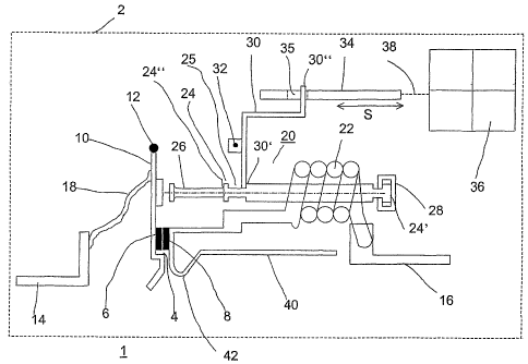
Figure 1 shows, schematically, a switching device 1
with a housing 2, an electromagnetic release 20 and a
switching mechanism 36 in the untripped state. Figure 2
shows the switching device shown in figure 1 in the
tripped state, identical or similarly functioning
assemblies or parts being designated by the same
reference numerals. A current path runs between an
input clamping piece 14 and an output clamping piece 16
via a movable litz wire 18, a contact lever 10, which
is mounted in a contact lever bearing 12, a contact
point 4, which comprises a movable contact piece 6,
which is located on the contact lever 10, and a fixed
contact piece 8, and a tripping coil 22. In the
switching position shown in figure 1, the contact point
4 is closed. A yoke 40 is also connected to the
tripping coil 22 and the fixed contact piece 8 via a
lug-shaped intermediate piece 42.
A thermal release, which is in addition still contained
in some switching devices and acts on the switching
mechanism in the event of the occurrence of an
overcurrent, with the result that said switching
mechanism then opens the contact point permanently, is
not illustrated.
The electromagnetic release 20 comprises the tripping
coil 22 and a tripping armature 24, which in this case
is in the form of a bar and is arranged in the interior
of the tripping coil 22 in such a way that the coil
longitudinal axis and the tripping armature
longitudinal axis coincide.
At a first, fixed end 24', the tripping armature 24 is
held in a tripping armature bearing 28, which is
connected to the housing 2. At its second, free end
24'', the tripping armature 24 is operatively connected
to a plunger 26. The operative connection is in this
case shown as an interlocking connection, but force-
CA 02624387 2008-04-01
WO 2007/057030 PCT/EP2005/012219
- 7 -
fitting or cohesive connections could also be realized
as an alternative.
At its free end 24'', the tripping armature 24 has a
notch 25 into which a tripping lever 30, which is
mounted in a tripping lever bearing 32, engages, for
example with a fork located at its first free end 30'.
The second free end 30'' of the tripping lever 30
engages in a cutout 35 in a slide 34, which is
operatively connected to the switching mechanism 36 via
a line of action 38.
The tripping armature 24 comprises a ferromagnetic
shape memory alloy based on nickel, manganese and
gallium. Such ferromagnetic shape memory alloys are
known in principle and are available; they are
manufactured and marketed, for example, by the Finnish
company AdaptaMat Ltd. A typical composition of
ferromagnetic shape memory alloys for the use according
to the invention in switching devices is provided by
the structural formula Ni6s-X-yMnzo+XGa1s+y, where x is
between 3 atomic percent and 15 atomic percent and y is
between 3 atomic percent and 12 atomic percent. The
ferromagnetic shape memory alloy used here has the
property that, in its martensitic phase, which is the
phase which the material assumes below the thermal
transition temperature, a transition between two
crystal structure variants of a twin crystal structure
takes place under the effect of an external magnetic
field on a microscopic scale, which transition is
macroscopically connected to a change in shape. In the
embodiment of the tripping armature selected here, the
change in shape consists in a linear expansion in the
direction of the bar longitudinal axis.
The thermal transition temperature in the case of the
ferromagnetic shape memory alloys used here is in the
region of room temperature and can be adjusted by
CA 02624387 2008-04-01
WO 2007/057030 PCT/EP2005/012219
- 8 -
varying the atomic percent contents of x and y within a
bandwidth. The working temperature range within which
the electromagnetic release functions can therefore be
adjusted within a bandwidth by selecting the material
composition.
If a high short-circuit current is flowing through the
switching device 2 in the event of a short circuit, the
tripping armature 24 as a result of the abovedescribed
effect expands, and as a result the plunger 26 strikes
the movable contact piece 6 so as to move it away from
the fixed contact piece 8, with the result that the
contact point 4 is opened and the switching device is
tripped, as illustrated in figure 2. The expansion of
the ferromagnetic shape memory material in this case
takes place very rapidly and virtually without any
delay. The delay time as the time difference between
the occurrence of the short-circuit current and the
maximum length expansion of the tripping armature 24 is
typically of the order of magnitude of 1 millisecond.
The tripping process is in this case assisted by the
tripping lever 30, which rotates in the clockwise
direction around the tripping lever bearing 32 when the
tripping armature 24 expands and, in the process,
displaces the slide 34 in its direction of longitudinal
extent, indicated by the direction arrow S, with the
result that the slide 34 actuates the switching
mechanism 36 via the line of action 38.
Once the switching device has been tripped, the current
path is interrupted and the magnetic field of the
tripping coil 22 collapses again. As a result, the
tripping armature 24 will contract to its initial
dimensions again, as a result of which the tripping
lever 30 is also moved back into the initial position
again, as shown in figure 1. The contact point 4 is now
held permanently in the open position through lines of
CA 02624387 2008-04-01
WO 2007/057030 PCT/EP2005/012219
- 9 -
action (not illustrated here) by means of the switching
mechanism 36.
Figure 3 shows a residual current circuit breaker in a
schematic illustration.
A schematic illustration of this arrangement can be
seen in figure 13. Primary conductors 61 and 62, which
have contact points 63 and 64, are passed through a
transformer core 60. A secondary winding 65 is arranged
around the transformer core 60, which secondary winding
65 is connected to a coil 66, in which a plunger 67
made of a material with a magnetic, but possibly also
with a magnetic and thermal shape memory effect passes
through. This plunger 67 acts on a switching mechanism
68 in the arrow direction P1 and, after the unlatching
process, the switching mechanism acts on the contact
points 63, 64 corresponding to the arrow direction P2.
In comparison with the arrangement shown in figure 1,
the plunger 67 in figure 1 has the reference numeral
24; the switching mechanism 68 in figure 1 has the
reference numeral 36, the coil 66 in the arrangement
shown in figure 1 has the reference numeral 22 and, as
can be seen, a plunger element 26 is missing because
direct action on the contact points 63, 64 in the case
of such a residual current circuit breaker is not
conventional.
Reference is now made to figure 4.
Figure 4 shows a contactor or parts of a contactor 70
with two fixed contact pieces 73 and 74, which are
arranged at a distance from one another, are arranged
on contact carriers 71 and 72 and are bridged by a
contact link 75, on which movable contact pieces 76, 77
are fitted. Figure 4 shows the contactor 70 in the
switched-on state when the contact pieces 73, 76; 74,
77 are in touching contact with one another.
CA 02624387 2008-04-01
WO 2007/057030 PCT/EP2005/012219
- 10 -
A plunger 78 made of a material with a magnetic shape
memory effect, which is in the form of an elongate
plunger whose one end is connected to the contact link
75 via a contact current spring 79 and whose other end
is held fixed in position in a mount 80, which is fixed
in a housing, is coupled to the contact link.
The plunger 78 is surrounded by an electromagnet system
81.
If the switch is now intended to be opened, the
material of the plunger deforms with the
electromagnetic shape memory effect; it is naturally
also possible in the normal state, i.e. in the
unstressed state, for the plunger 78 to be arranged in
such a way that the contact points 73/76; 74/77 are
open. As a result of a control current, the plunger
will then expand owing to the magnetic field produced
by the coil 81 as a result of the magnetic shape memory
effect and will close the contact points, the contact
compression spring 79 conventionally being compressed
slightly during the switch-on process.
In the embodiment shown in figure 5, a plunger 82 made
of a material with a magnetic shape memory effect is
surrounded by a coil 83, the coil 83 being supplied
with current via feed lines 84 and 85 via a high-pass
filter, which is formed from a capacitor 86 and a
resistor 87. If the plunger 82 expands as a result of
the magnetic field, it actuates a contact lever 88 and
opens a contact point 91, which is formed from a
contact piece 89, which is fitted on a movable contact
lever 88, and a fixed contact piece 90.
Figure 6 shows a view into a line circuit breaker, only
the parts which are important to the invention being
illustrated.
CA 02624387 2008-04-01
WO 2007/057030 PCT/EP2005/012219
- 11 -
The line circuit breaker overall has the reference
numeral 92 with a front face 93, from which the
switching handle 94 of a toggle switch 96, which is
mounted rotatably at 95, protrudes. The switching
handle 94 is integrally formed on a rotatable hub 97.
At 98, a plunger 99 is articulated on the hub 97, which
plunger 99 is coupled to an elongate element 100 made
of a material with a magnetic shape memory effect. The
element 100 is surrounded by a coil 101 and, when a
current flows through, the= length of the element 100
changes, with the result that the plunger 99 actuates
the hub 97 and therefore the switching handle 94. Since
the switching handle is conventionally linked and
connected to the switching mechanism in the case of a
line circuit breaker, in this way the switching device
is switched on via the element 100 with the plunger 99.