Note: Descriptions are shown in the official language in which they were submitted.
CA 02624778 2008-04-03
WO 2007/133271 PCT/US2006/048457
METHODS FOR ORIENTED GROWTH OF NANOWIRES ON
PATTERNED SUBSTRATES
STATEMENT REGARDING FEDERALLY SPONSORED RESEARCH
[0001] Portions of this invention may have been made with United States
Government support under a grant from the National Science Foundation,
Grant No. IIP-0620589. As stich, the United States Government may have
certain rights in this invention.
BACKGROUND OF THE INVENTION
Field of the Invention
[0002] The present invention relates to nanowires, and more particularly, to
nanowire growth and harvesting.
Background of the Invention
[0003] Nanostructures, and in particular, nanowires have the potential to
facilitate a whole new generation of electronic devices. A major impediment
to the emergence of this new generation of electronic devices based on
nanostructures is the ability to effectively grow and harvest nanowires and
other nanostructures that have consistent characteristics. Current approaches
to grow and harvest nanowires do not facilitate mass production and do not
yield consistent nanowire performance characteristics.
[0004] What are needed are systems and methods to grow and harvest
nanowires that have consistent performance characteristics.
CA 02624778 2008-04-03
WO 2007/133271 PCT/US2006/048457
-2-
SUIVIMARY OF THE INVENTION
[0005] The present invention provides methods for producing nanowires. In
one embodiment, one or more nucleating particles are deposited on a substrate
material. Then, the nucleating particles are heated to a first temperature and
then contacted with a first precursor gas mixture to create a liquid alloy
droplet and initiate nanowire growth. The alloy droplet is then heated to a
second temperature and then contacted with a second precursor gas mixture,
whereby nanowires are grown at the site of the alloy droplet. The substrate
material utilized in the processes of the present invention may be
crystallographic or amorphous. Suitably, the substrate material comprises
crystallographic silicon, either polycrystalline or single crystalline. In
other
embodiments, the substrate may be amorphous SiOa, Si3N4, or alumina.
[0006] Additional methods for producing nanowires (e.g., Si nanowires) are
also provided by the present invention. For example, such methods include
depositing one or more nucleating particles (e.g., a metal catalyst such as
gold
nanoparticles) on a substrate material (or nucleating nanoparticles on a
substrate surface (e.g., by heating a gold film coating layer on the
surface)).
The nucleating particles are then heated to a first temperature at which a
first
precursor gas decomposes to form a eutectic phase with the nucleating
particles and then the nucleating particles are contacted with the first
precursor
gas mixture, wherein the first precursor gas mixture comprises a first
precursor
gas comprising at least one atomic species (e.g., Cl) that assists in
orienting
the growing nanowires (e.g., by etching as described in more detail below).
The nucleating particles are then contacted with a second precursor gas
mixture a.fter initiation of nanowire growth, wherein the second precursor gas
mixture includes a precursor gas that decomposes to form a eutectic phase
with the nucleating particles at a second temperature which is lower than the
first temperature, and heating the nucleating particles to the second
temperature.
CA 02624778 2008-04-03
WO 2007/133271 PCT/US2006/048457
-3-
[00071 The above method can be reversed such that the process of nanowire
growth is initiated with a precursor gas at the lower temperature, and then
nanowire growth is continued at a higher temperature using a second precursor
gas (e.g., a gas having a reactive etchant species to aid in nanowire
orientation
such as chlorine). The first precursor gas utilized is preferably SiC14 or
SiHzC12 which contains Si and Cl atoms upon disassociation at the first
temperature. The Si atoms provide for nanowire growth and the Cl atoms
allow for growth of the wires in a <111> orientation when grown on a
crystallographic substrate as a result of etching of the native oxide layer on
the
silicon substrate. Once nanowire growth has been initiated, a second
precursor gas mixture including a precursor gas such as SiH4 or Si2H6 can be
introduced which decomposes to form a eutectic phase with the nucleating
particles at a lower temperature than the first precursor gas. The
disassociated
Si atoms from SiH4 or Si2H6 at the second temperature continue the growth of
the Si nanowires. Thus, nanowire growth can continue with the free Si atoms
at a lower temperature than that at which nanowire growth is initiated, e.g.,
allowing growth of the oriented wires to a desired length while minimizing
diffusion of the metal catalyst into the growing nanowires.
100081 The substrate material utilized in these methods may be
crystallographic or amorphous. Suitably, the substrate material comprises
crystallographic silicon, either polycrystalline or single crystalline. In
other
embodiments, the substrate may be amorphous Si02, Si3N4, or alumina
[0009] In embodiments where crystalline substrates are utilized, the wires
growing on the substrate material can preferably grow in an epitaxial
orientation. Nanowires produced according to the processes of the present
invention grow out of the plane of the substrate material, and are capable of
transporting electrical charge.
[00010] In certain suitable embodiments of the methods of the present
invention, the first temperature to which the nucleating particles is heated
is
higher than the second temperature to which the alloy droplet is heated.
Suitably, the first temperature is at least about 50 C higher than the second
CA 02624778 2008-04-03
WO 2007/133271 PCT/US2006/048457
-4-
temperature. The nucleating particles used in the practice of the present
invention will suitably be a metal catalyst and will comprise a metal that
reacts
with both the first precursor gas mixture and the second precursor gas mixture
(i.e., decomposed first and second precursor gas mixtures) to form a eutectic
from which Si may precipitate. Suitable metal catalysts comprise Au, Pt, Fe,
Ti, Ga, Ni, Sn or In and in certain such embodiments, may be a Au colloid or
Au film.
[00011] The first precursor gas mixture and the second precursor gas mixture
utilized in the processes of the present invention will suitably comprise
SiH4,
Si2H6, SiC14 or SiH2C12, and may further comprise B2H6, trimethyl boron
(TMB), POC13 or PH3 (e.g., as dopant materials). Additional embodiments of
the processes of the present invention may further comprise contacting the
growing nanowires with one or more additional precursor gas mixtures
comprising SiH4, Si2H6, SiC14 or SiHaC12 and further comprising B2H6, T1VIB,
POC13 or PH3 to grow the nanowires to a desired length. The precursor gases
used in the processes of the present invention may also suitably be introduced
via plasma enhanced sputter deposition.
[00012] In another embodiment of the present invention, the need for growing
nanowires at different temperatures can be avoided by growing the nanowires
at lower temperatures (e.g., lower than about 800 C) using Plasma Enhanced
Sputter Deposition (or Plasma Enhanced Chemical Vapor Deposition
(PECVD)). In this embodiment, the nucleating particles are contacted with a
precursor gas mixture that preferably includes a precursor gas comprising, a
reactive species (e.g., Cl) that aids in orienting the growing nanowires, such
as
SiCla or SiH2C12. Alternatively, the precursor gas mixture may include
chlorine gas (or plasma) from a separate, independent source that can be
provided- in combination with one or more of the precursor gases discussed
above (e.g., SiH4, Si2H6, SiC14 or SiHZCIz). Where the precursor gas mixture
includes SiC14 or SiH2C12, decomposition of SiC14 or SiH2Cl2 into Si and Cl in
the presence of a carrier gas (e.g., Ha, H2Ar) forms HCI. As discussed in more
detail below, this creates a competition between etching with HCI and growth
CA 02624778 2008-04-03
WO 2007/133271 PCT/US2006/048457
-5-
from the Si vapor. Chlorine aids in removal of interfacial oxide on Si
substrates leading to the oriented nanowire growth. The addition of an
independent source of chlorine gas has the advantage of allowing the reactive
species of Si and Cl to be independently controlled in the plasma to enhance
or
suppress etching as needed to promote nanowire growth. Sputter deposition
can, be accomplished via any method known to the ordinarily skilled artisan,
for example, diode, radio frequency and direct current deposition.
[000131 The present invention also provides methods for producing nanowires
which do not involve metal catalysts, including, for example, hydroxylating a
substrate material, contacting the substrate material with a first precursor
gas
mixture, forming one or more nuclei (e.g., nanoparticles) on a surface of the
substrate material, contacting the nuclei with a second precursor gas mixture,
and growing nanowires at the site of the one or more nuclei.
[00014] In another aspect of the invention, additional methods for nanowire
synthesis are provided. In an embodiment, a method for nanowire synthesis
includes positioning a granular precursor material at one end of a vessel at
one
temperature and positioning catalyst particles at an opposite end of the
vessel
at another temperature. Materials are then transferred from one end of the
vessel to another. A transport agent is reacted with the granular nanowire
precursor material to form nanowires. In an alternative embodiment, a similar
method is provided to dope nanowires_
[00015] In a further aspect of the invention, methods to improve nanowire
quality during manufacturing are provided. In particular, a method to reduce
surface states from dangling bonds on a nanowire structure is provided. In an
embodiment, the method includes creating a nanowire structure, depositing a
sacrificial layer on the nanowire structure, passivating the nanowire
structure
with the sacrificial layer, and chemically removing the sacrificial layer to
free
the nanowires.
[00016] In another embodiment, a method for producing a nanowire device is
disclosed that includes providing a substrate having nanowires attached to a
surface in a vertical orientation, depositing a dielectric layer on the
surface of
CA 02624778 2008-04-03
WO 2007/133271 PCT/US2006/048457
-6-
the nanowires, depositing one or more nanowire contacts on the nanowires,
depositing a material over the nanowires to form a nanowire composite, and
separating the nanowire composite from the substrate.
[00017] A series of methods are also provided for harvesting nanowires. In an
embodiment, a method includes growing a nanowire with a desired portion
and a sacrificial portion. The desired portion has different properties than
those of the sacrificial portion. In one example, the sacrificial portion is
an
alloy and the desired portion is not. In another example, the sacrificial
portion
is doped differently than the desired portion. Wet etchants are used to
differentially remove the sacrificial portion of the nanowires. The example
wet etchants etch away the sacrificial portion of the nanowire at a far
greater
rate than the desired portion. As a result, nanowires can be produced with
consistent lengths.
[00018] In another embodiment, silicon nanowires are grown on a silicon
substrate in which the orientation of the silicon in the nanowires is
different
from the orientation of the silicon in the substrate. For example, the atoms
in
the silicon nanowires can have Miller indices of 111, while the silicon atoms
in the substrate can have Miller indices of 100. As in the previous case, wet
etchants can be used to differentially remove portions of the silicon
substrate
to free the nanowires.
[00019] In another aspect of the invention, methods for transferring nanowires
from one substrate to another substrate are provided. The methods can be
used, for example, to transfer nanowires from a nanowire growth substrate to a
device substrate. In an embodiment, the method includes coating a transfer
surface with a non-stick coating, such as TEFLON. The transfer surface can
then be pressed against nanowires that are affixed to a nanowire growth
substrate. The nanowires become stuck to the transfer surface with the non-
stick coating. The transfer surface is then positioned over a device
substrate,
and pressure is applied to the back of the transfer surface to release the
nanowires onto the device substrate. In altexnative embodiments, the transfer
surface can be patterned with a non-stick coating to match areas on a device
CA 02624778 2008-04-03
WO 2007/133271 PCT/US2006/048457
-7-
substrate where nanowires are to be placed. In a similar alternative
embodiment, the non-stick coating can be distributed all over the transfer
surface, and pressure can be placed on the backside of the transfer surface in
a
patterned fashion to release nanowires onto particular areas. of a device
substrate.
(00020] In an additional embodiment, methods for harvesting and transferring
nanowires are disclosed that include providing a substrate material having one
or more nanowires attached to a top surface. A transfer substrate is then
provided, oriented above the top surface of the substrate. Pressure is applied
to
the transfer substrate, such that the transfer substrate is brought in'
contact with
the one or more nanowires. One or more of the nanowires are then transferred
from the substrate to the transfer substrate, and the transfer substrate is
then
removed. In this embodiment, the transfer substrate can be a flexible polymer
and a probe can be used to apply pressure. In embodiments the probe may be
heated or the substrate may be heated.
[00021] In a further embodiment, the present invention provides methods for
producing nanowires on patterned substrates. In suitable embodiments, the
methods comprise layering a catalyst-repelling material on a substrate
material
to at least partially cover the substrate material. One or more nucleating
particles are then deposited on the substrate material. The nucleating
particles
are then heated to a first temperature and contacted with a first precursor
gas
mixture to create a liquid alloy droplet to initiate nanowire growth. The
alloy
droplet is then heated to a second temperature and the alloy droplet is then
contacted with a second precursor gas mixture, whereby nanowires are grown
at the site of the alloy droplet. Suitably, the substrate material will
comprise a
crystallographic material, such as Si, and the nucleating particles will
comprise metallic films or colloids, such as films or colloids comprising Au,
Al, Pt, Fe, Ti, Ga, Ni, Sn or In. Examples of catalyst-repelling material
include, but are not limited to, Si02, and anodic alumina. As noted
throughout, the temperature and precursor gases can be varied throughout the
growth process, suitably starting at a higher -temperature initially, and then
CA 02624778 2008-04-03
WO 2007/133271 PCT/US2006/048457
-8-
using a lower temperature for continued nanowire growth. Examples of
precursor gas mixtures for use in the methods of the present invention
include,
but are not limited to, SiH4, SiCl4 and SiH2Cl2. The present invention also
provides nanowires produced by the methods of the present invention and
electronic devices comprising such nanowires.
[00022] Additional methods for producing nanowires on patterned substrates
are also provided. Suitably, a catalyst-repelling material is applied on a
substrate material to at least partially cover the substrate material. Then,
one
or more nucleating particles are applied on the substrate material. The
nucleating particles are then heated (e.g., to a temperature of above about
400 C) and then contacted with a precursor gas mixture (e.g., at a pressure of
above about 0.5 torr) to create an alloy droplet, whereby nanowires are grown
at the site of the alloy droplet. Suitably, the catalyst-repelling material
(e.g.,
Si02 or anodic alumina) comprises at least one void that does not cover the
substrate material (e.g., a silicon or other crystallographic substrate). In
exemplary embodiments, nucleating particles are deposited on the catalyst-
repelling material (e.g., in the form of a film or colloid and then heated),
wherein the nucleating particles deposit on the substrate material at the site
of
the at least one void.
[00023] In exemplary embodiments, the methods of the present invention
comprise heating to a temperature of about 450 C to about 700 C, at a
pressure of about 5 to about 200 torr, suitably about 45 torr. Exemplary
nucleating particles include those disclosed throughout, such as metals
comprising Au, Al, Pt, Fe, Ti, Ga, Ni, Sn or In. Exemplary precursor gas
mixtures include those disclosed throughout, such as gas mixtures comprising
SiH4, Si2H6, SiC14 or SiH2C12.
[00024] The present invention also provides additional methods for producing
nanowires. For example, one or more nucleating particles (e.g., metallic
colloids or films) are be applied on a substrate material. Then, the
nucleating
particles are heated to a temperature of greater than about 400 C (suitably,
between about 450 C to about 700 C), and contacted with a precursor gas
CA 02624778 2008-04-03
WO 2007/133271 PCT/US2006/048457
-9-
mixture at a pressure greater than about 0.5 torr (suitably between about 5 to
about 200 torr, more suitably about 45 torr) to create a liquid alloy droplet,
whereby nanowires are grown at the site of the alloy droplet.
[00025] Exemplary nucleating particles include those disclosed throughout,
such as metals comprising Au, Al, Pt, Fe, Ti, Ga, Ni, Sn or In. Exemplary
precursor gas mixtures include those disclosed throughout, such as gas
mixtures comprising SiH4, Si2H6, SiC14 or SiHZCIz.
[00026] Further embodiments, features, and advantages of the invention, as
well as the structure and operation of the various embodiments of the
invention are described in detail below with reference to accompanying
drawings.
BRIEF DESCRIPTION OF THE FIGURES
[00027] The invention is described with reference to the accompanying
drawings. In the drawings, like reference numbers indicate identical or
functionally similar elements. The drawing in which an element first appears
is indicated by the left-most digit in the corresponding reference number.
[00028] FIG. 1A is a diagram of a single crystal semiconductor nanowire.
[00029] FIG. 1B is a diagram of a nanowire doped according to a core-shell
structure.
[00030] FIG. 2 is a flowchart of a method for preparing nanowires using a
combination of Si precursors, according to an embodiment of the invention.
[00031] FIG. 3 is a flowchart of a method for preparing nanowires using a
combination of Si precursors, according to an embodiment of the invention.
[00032] FIG. 4 is a flowchart of a method for nanowire synthesis, according to
an embodiment of the invention.
[00033] FIG. 4A is a diagram of a nanowire synthesis vessel, according to an
embodiment of the invention.
[00034] FIG. 5 is a flowchart of a method for doping nanowires, according to
an embodiment of the invention.
CA 02624778 2008-04-03
WO 2007/133271 PCT/US2006/048457
-10-
[000351 FIG. 6 is a flowchart of a method for reducing surface states from
dangling bonds on a nanowire structure, according to an embodiment of the
invention.
1000361 FIG. 7 is a diagram of a nanowire coated with a sacrificial layer,
according to an embodiment of the invention.
[00037] FIG. 8 is a diagram showing nanowire processing in accordance with
. one embodiment of the present invention.
[00038] FIG. 9 is a diagram showing nanowire processing following transfer in
accordance with one embodiment of the present invention.
[00039] FIG. 10 is a flowchart of a method of harvesting a nanowire using a
sacrificial portion, according to an embodiment of the invention.
[00040] FIG. 11 is a diagram of a nanowire with a sacrificial portion,
according
to an embodiment of the invention.
[00041] FIG. 12 is a flowchart of a method of harvesting a nanowire by
monitoring of a PN junction, according to an embodiment of the invention.
[00042] FIG. 13 is a flowchart of a method of harvesting a nanowire using a
sacrificial metal layer on a nanowire growth substrate, according to an
embodiment of the invention.
[00043] FIG. 14 is a diagram of a nanowire grown on a sacrificial metal layer
on a nanowire growth substrate, according to an embodiment of the invention.
[00044] FIG. 15 is a flowchart of a method of harvesting an Si nanowire when
using a non-Si substrate; according to an embodiment of the invention.
[00045] FIG. 16 is a flowchart of a method of harvesting a nanowire with one
orientation when a nanowire growth substrate with a different orientation is
used, according to an embodiment of the invention.
[00046] FIG. 17 is a diagram of a nanowire with one orientation growing on a
nanowire growth substrate with a different orientation, according to an
embodiment of the invention.
[00047] FIG. 18 is a flowchart of a method for transferring nanowires from a
first substrate to a second substrate, according to an embodiment of the
invention.
CA 02624778 2008-04-03
WO 2007/133271 PCT/US2006/048457
-11-
[00048] FIG. 19 is a flowchart of a method for transferring nanowires from a
first substrate with a patterned coating to a second substrate, according to
an
embodiment of the invention.
[00049] FIG. 20A is a diagram of a first substrate with nanowires and a
transfer
substrate, according to an embodiment of the invention.
[00050] FIG. 20B is a diagram of a device substrate and a transfer substrate
transferring nanowires, according to an embodiment of the invention.
[000511 FIG. 21 is a representation of probe nanowire transfer scheme in
accordance with one embodiment of the present invention.
[00052] FIG. 22 is a representation of global nanowire transfer in accordance
with one embodiment of the present invention.
[00053] FIGs. 23A is a transmission electron micrograph that shows a substrate
with e-field oriented nanowires prior to transfer, according to an embodiment
of the invention.
[00054] FIG. 23B is a transmission electron micrograph that shows nanowires
remaining on substrate following transfer, according to an embodiment of the
invention.
[00055] FIG. 23C is a transmission electron micrograph that shows nanowires
on transfer substrate following transfer, according to an embodiment of the
invention.
[00056] FIG. 24 is a diagram showing oriented nanowire growth using a
patterned substrate in accordance with one embodiment of the present
invention.
[00057] FIG. 25 is a flowchart of a method for preparing nanowires on a
patterned substrate accordance with one embodiment of the present invention.
[00058] FIG. 26 is a flowchart of a method for preparing nanowires in
accordance with one embodiment of the present invention.
CA 02624778 2008-04-03
WO 2007/133271 PCT/US2006/048457
-12-
DETAILED DESCRIPTION OF THE INVENTION
[00059] It should be appreciated that the particular implementations shown and
described herein are examples of the invention and are not intended to
otherwise limit the scope of the present invention in any way. Indeed, for the
sake of brevity, conventional electronics, manufacturing, semiconductor
devices, and nanowire (NW), nanorod, nanotube, and nanoribbon technologies
and other functional aspects of the systems (and components of the individual
operating components of the systems) may not be described in detail herein.
Furtherrnore, for purposes of brevity, the invention is frequently described
herein as pertaining to nanowires.
(00060] It should be appreciated that although nanowires are frequently
referred to, the techniques described herein are also applicable to other
nanostructures, such as nanorods, nanotubes, nanotetrapods, nanoribbons
and/or combinations thereof. It should further be appreciated that the
manufacturing techniques described herein could be used to create any
semiconductor device type, and other electronic component types. Further,
the techniques would be suitable for application in electrical systems,
optical
systems, consumer electronics, industrial electronics, wireless systems, space
applications, or any other application.
[00061] As used herein, an "aspect ratio" is the length of a first axis of a
nanostructure divided by the average of the lengths of the second and third
axes of the nanostructure, where the second and third axes are the two axes
whose lengths are most nearly equal to each other. For example, the aspect
ratio for a perfect rod would be the length of its long axis divided by the
diameter of a cross-section perpendicular to (normal to) the long axis.
[00062] The term "heterostructure" when used with reference to nanostructures
refers to nanostructures characterized by at least two different and/or
distinguishable material types. Typically, one region of the nanostructure
comprises a first material type, while a second region of the nanostructure
comprises a second material type. In certain embodiments, the nanostructure
CA 02624778 2008-04-03
WO 2007/133271 PCT/US2006/048457
-13-
comprises a core of a first material and at least one shell of a second (or
third
etc.) material, where the different material types are distributed radially
about
the long axis of a nanowire, a long axis of an arm of a branched nanocrystal,
or the center of a nanocrystal, for example. A shell need not completely cover
the adjacent materials to be considered a shell or for the nanostructure to be
considered a heterostructure. For example, a nanocrystal characterized by a
core of one material covered with small islands of a secorid material is a
heterostructure. In other embodiments, the different material types are
distributed at different locations within the nanostructure. For example,
material types can be distributed along the major (long) axis of a nanowire or
along a long axis of arm of a branched nanocrystal. Different regions within a
heterostructure can comprise entirely different materials, or the different-
regions can comprise a base material.
[00063] As used herein, a "nanostructure" is a structure having at least one
region or characteristic dimension with a dimension of less than about 500 nm,
e.g., less than about 200 nm, less than about 100 nm, less than about 50 nm,
or
even less than about 20 nm. Typically, the region or characteristic dimension
will be along the smallest axis of the structure. Examples of such structures
include nanowires, nanorods, nanotubes, branched nanocrystals,
nanotetrapods, tripods, bipods, nanocrystals, nanodots, quantum dots,
nanoparticles, branched tetrapods (e.g., inorganic dendrimers), and the like.
Nanostructures can be substantially homogeneous in material properties, or in
certain embodiments can be heterogeneous (e.g., heterostructures).
Nanostructures can be, for example, substantially crystalline, substantially
monocrystalline, polycrystalline, amorphous, or a combination thereof. In one
aspect, each of the three dimensions of the nanostructure has a dimension of
less than about 500 nm, for example, less than about 200 nm, less than about
100 nm, less than about 50 nm, or even less than about 20 nm.
[00064] As used herein, the term "nanowire" generally refers to any elongated
conductive or semiconductive material (or other material described herein)
that includes at least one cross sectional dimension that is less than 500nrn,
CA 02624778 2008-04-03
WO 2007/133271 PCT/US2006/048457
-14-
and preferably, less than 100 nm, and has an aspect ratio (length:width) of
greater than 10, preferably greater than 50, and more preferably, greater than
100.
[00065] The nanowires of this invention can be substantially homogeneous in
material properties, or in certain' embodiments can be heterogeneous (e.g.
nanowire heterostructures). The nanowires can be fabricated from essentially
any convenient material or materials, and can be, e.g., substantially
crystalline,
substantially monocrystalline, polycrystalline, or amorphous. Nanowires can
have a variable diameter or can have a substantially uniform diameter, that
is,
a diameter that shows a variance less than about 20% (e.g., less than about
10%, less than about 5%, or less than about 1%) over the region of greatest
variability and over a linear dimension of at least 5 nm (e.g., at least 10
nm, at
least 20 nm, or at least 50 nm). Typically the diameter is evaluated away from
the ends of the nanowire (e.g. over the central 20%, 40%, 50%, or 80% of the
nanowire). A nanowire can be straight or can be e.g. curved or bent, over the
entire length of its long axis or a portion thereof. In certain embodiments, a
nanowire or a portion thereof can exhibit two- or three-dimensional quantum
confinement. Nanowires according to this invention can expressly exclude
carbon nanotubes, and, in certain embodiments, exclude "whiskers" or
"nanowhiskers", particularly whiskers having a diameter greater than 100 nm,
or greater than about 200 nm.
[00066] Examples of such nanowires include semiconductor nanowires as
described in Published International Patent Application Nos. WO 02/17362,
WO 02/48701, and WO 01/03208, carbon nanotubes, and other elongated
conductive or semiconductive structures of like dimensions, which are
incorporated herein by reference.
[00067] As used herein, the term "nanorod" generally refers to any elongated
conductive or semiconductive material (or other material described herein)
similar to a nanowire, but having an aspect ratio (length:width) less than
that
of a nanowire. Note that two or more nanorods can be coupled together along
their longitudinal axis so that the coupled nanorods span all the way between
CA 02624778 2008-04-03
WO 2007/133271 PCT/US2006/048457
-15-
electrodes. Alternatively, two or more nanorods can be substantially aligned
along their longitudinal axis, but not coupled together, such that a small gap
exists between the ends of the two or more nanorods. In this case, electrons
can flow from one nanorod to another by hopping from one nanorod to
another to traverse the small gap. The two or more nanorods can be
substantially aligned, such that they form a path by which electrons can
travel
between electrodes.
[00068] A wide range of types of materials for nanowires, nanorods, nanotubes
and nanoribbons can be used, including semiconductor material selected from,
e.g., Si, Ge, Sn, Se, Te, B', C (including diamond), P, B-C, B-P(BP6), B-Si,
Si-
C, Si-Ge, Si-Sn and Ge-Sn, SiC, BNlBP/BAs, AIN, A1P, AlAs, AlSb, GaN,
GaP, GaAs, GaSb, InN, InP, InAs, InSb, ZnO, ZnS, ZnSe, ZnTe, CdS, CdSe,
CdTe, HgS, HgSe, HgTe, BeS, BeSe, BeTe, MgS, MgSe, GeS, GeSe, GeTe,
SnS, SnSe, SnTe, PbO, PbS, PbSe, PbTe, CuF, CuCI, CuBr, Cul, AgF, AgCI,
AgBr, AgT, BeSiN2, CaCN2, ZnGeP2, CdSnAs2, ZnSnSb2, CuGeP3, CuSi2P3,
(Cu, Ag)(Al, Ga, In, Tl, Fe)(S, Se, Te)2, Si3N4, Ge3N4, A1203, (Al, Ga, In)z
(S,
Se, = Te)3, A12CO, and. an appropriate combination of two or more such
semiconductors.
[00069] The nanowires can also be formed from other materials such as metals
such as gold, nickel, palladiurn, iridium, cobalt, chromium, aluminum,
titanium, tin and the like, metal alloys, polymers, conductive polymers,
ceramics, and/or combinations thereof. Other now known or later developed
conducting or semiconductor materials can be employed.
[00070] In certain aspects, the semiconductor may comprise a dopant from a
group consisting of: a p-type dopant from Group III of the periodic table; an
n-
type dopant from Group V of the periodic table; a p-type dopant selected from
a group consisting of: B, Al and In; an n-type dopant selected from a group
consisting of: P, As and Sb; a p-type dopant from Group II of the periodic
table; a p-type dopant selected from a group consisting of= Mg, Zn, Cd and
Hg; a p-type dopant from Group IV of the periodic table; a p-type dopant
selected from a group consisting of: C and Si.; or an n-type dopant selected
CA 02624778 2008-04-03
WO 2007/133271 PCT/US2006/048457
-16-
from a group consisting of: Si, Ge, Sn, S, Se and Te. Other now known or
later developed dopant materials can be employed.
[00071] Additionally, the nanowires or nanoribbons can include . carbon
nanotubes, or nanotubes formed of conductive or semiconductive organic
polymer materials, (e.g., pentacene, and transition metal oxides).
[00072] Hence, although the term "nanowire" is referred to throughout the
description herein for illustrative purposes, it is intended that the
description
herein also encompass. the use of nanotubes (e.g., nanowire-like structures
having a hollow tube formed axially therethrough). Nanotubes can be formed
in combinations/thin films of nanotubes as is described herein for nanowires,
alone or in combination with nanowires, to provide the properties and
advantages described herein.
[00073] It should be understood that the spatial descriptions (e.g., "above",
"below", "up", "down", "top", "bottom," etc.) made herein are for purposes of
illustration only, and that devices of the present invention can be spatially
arranged in any orientation or manner. In addition, there may also be
intervening layers or materials present in such devices to facilitate
processing.
Types of'luanowires and Their Synthesis
[00074] FIG. lA illustrates a single crystal semiconductor nanowire core
(hereafter "nanowire") 100. FIG. 1 A shows a nanowire 100 that is a uniformly
doped single crystal nanowire. Such single crystal nanowires can be doped
into either p- or n-type semiconductors in a fairly controlled way. Doped
nanowires such as nanowire 100 exhibit improved electronic properties. For
instance, such nanowires can be doped to have carrier mobility levels
comparable to bulk single crystal materials.
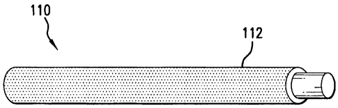
[00075] FIG. 1B shows a nanowire 110 doped according to a core-shell
structure. As shown in FIG. 1B, nanowire 110 has a doped surface layer 112,
which can have varying thickness levels, including being only a molecular
monolayer on the surface of nanowire I 10.
CA 02624778 2008-04-03
WO 2007/133271 PCT/US2006/048457
-17-
[00076] The valence band of the insulating shell can be lower than the valence
band of the core for p-type doped wires, or the conduction band of the shell
can be higher than the core for n-type doped wires. Generally, the core
nanostructure can be made from any metallic or semiconductor material, and
the shell can be made from the same or a different material. For example, the
first core material can comprise a first semiconductor selected from the group
consisting of: a Group II-VI semiconductor, a Group III-V semiconductor, a
Group IV semiconductor, and an alloy thereof. Similarly, the second material
of the shell can comprise a second semiconductor, the same as or different
from the first semiconductor, e.g., selected from the group consisting of: a
Group II-VI semiconductor, a Group III-V semiconductor, a Group IV
semiconductor, and an alloy thereof. Example semiconductors include, but
are not limited to, CdSe, CdTe, InP, InAs, CdS, ZnS, ZnSe, ZnTe, HgTe,
GaN, GaP, GaAs, GaSb, InSb, Si, Ge, AlAs, AlSb, PbSe, PbS, and PbTe. As
noted above, metallic materials such as gold, chromium, tin, nickel, aluminum
etc. and alloys thereof can be used as the core material, and the metallic
core
can be overcoated with an appropriate shell material such as silicon dioxide
or
other insulating materials
[00077] , Nanostructures can be fabricated and their size can be controlled by
any of a number of convenient methods that can be adapted to different
materials. For example, synthesis of nanocrystals of various composition is
described in, e.g., Peng et al. (2000) "Shape Control of CdSe Nanocrystals"
Nature 404, 59-61; Puntes et al. (2001) "Colloidal nanocrystal shape and size
control: The case of cobalt" Science 291, 2115-2117; USPN 6,306,736 to
Alivisatos et al. (October 23, 2001) entitled "Process for forming shaped
group III-V semiconductor nanocrystals, and product formed using process";
USPN 6,225,198 to Alivisatos et al. (May 1, 2001) entitled "Process for
forming shaped group II-VI semiconductor nanocrystals, and product formed
using process"; USPN 5,505,928 to Alivisatos et al. (April 9, 1996) entitled
"Preparation of Ill-V semiconductor nanocrystals"; USPN 5,751,018 to
Alivisatos et al. (May 12, 1998) erititled "Semiconductor nanocrystals
CA 02624778 2008-04-03
WO 2007/133271 PCT/US2006/048457
-18-
covalently bound to solid inorganic surfaces using self-assembled
monolayers"; USPN 6,048,616 to Gallagher et al. (April 11, 2000) entitled
"Encapsulated quantum sized doped semiconductor particles and method of
manufacturing same"; and USPN 5,990,479 to Weiss et al. (November 23,
1999) entitled "Organo luminescent semiconductor nanocrystal probes for
biological applications and process for making and using such probes."
[00078] Growth of nanowires having various aspect ratios, including nanowires
with controlled diameters, is described in, e.g., Gudiksen et al (2000)
"Diameter-selective synthesis of semiconductor nanowires" J. Am. Chem.
Soc. 122, 8801-8802; Cui et al. (2001) "Diameter-controlled synthesis of
single-crystal silicon nanowires" Appl. Phys. Lett. 78, 2214-2216; Gudiksen et
al. (2001) "Synthetic control of the diameter and length of single crystal
semiconductor nanowires" J. Phys. Chem. B 105,4062-4064; Morales et al.
(1998) "A Iaser ablation method for the synthesis of crystalline semiconductor
nanowires" Science 279, 208-211; Duan et al. (2000} "General synthesis of
compound semiconductor nanowires" Adv. Mater. 12, 298-302; Cui et al.
(2000) "Doping and electrical transport in silicon nanowires" J. Phys. Chem.
B 104, 5213-5216; Peng et al. (2000) "Shape control of CdSe nanocrystals"
Nature 404, 59-61; Puntes et al. (2001) "Colloidal nanocrystal shape and size
control: The case of cobalt" Science 291, 2115-2117; USPN 6,306,736 to
Alivisatos et al. (October 23, 2001) entitled "Process for forming shaped
group Ill-V semiconductor nanocrystals, and product formed using process";
USPN 6,225,198 to Alivisatos et al. (May 1, 2001) entitled "Process for
forming shaped group II-VI semiconductor nanocrystals, and product formed
using process"; USPN 6,036,774 to Lieber et al. (March 14, 2000) entitled
"Method of producing metal oxide nanorods"; USPN 5,897,945 to Lieber et
al. (April 27, 1999) entitled "Metal oxide nanorods"; USPN 5,997,832 to
Lieber et al. (December 7, 1999) "Preparation of carbide nanorods"; Urbau et
al. (2002) "Synthesis of single-crystalline perovskite nanowires composed of
barium titanate and strontium titanate" J. Am. Chem. Soc., 124, 1186; and
CA 02624778 2008-04-03
WO 2007/133271 PCT/US2006/048457
-19-
Yun et al. (2002) "Ferroelectric Properties of Individual Barium Titanate
Nanowires Investigated by Scanned Probe Microscopy" Nanoletters 2, 447.
[00079] Growth of branched nanowires (e.g., nanotetrapods, tripods, bipods,
and ;branched tetrapods) is described in, e.g., Jun et al. (2001) "Controlled
synthesis of multi-armed CdS nanorod architectures using monosurfactant
system" J. Am. Chem. Soc. 123, 5150-5151; and Manna et al. (2000)
"Synthesis of Soluble and Processable Rod-,Arrow-, Teardrop-, and Tetrapod-
Shaped CdSe Nanocrystals" J. Am. Chem. Soc. 122, 12700-12706.
[00080] Synthesis of nanoparticles is described in, e.g., USPN 5,690,807 to
Clark Jr. et al. (November 25, 1997) entitled "Method for producing.
semiconductor particles"; USPN 6,1.36,156 to El-Shall, et al. (October 24,
2000) entitled "Nanoparticles of silicon oxide alloys"; USPN 6,413,489 to
Ying et al. (July 2, 2002) entitled "Synthesis of nanometer-sized particles by
reverse micelle mediated techniques"; and Liu et al. (2001) "Sol-Gel Synthesis
of Free-Standing Ferroelectric Lead Zirconate Titanate Nanoparticles" J. Am.
Chem. Soc. 123, 4344. Synthesis of nanoparticles is also described in the
above citations for growth of nanocrystals, nanowires, and branched
nanowires, where the resulting nanostructures have an aspect ratio less than
about 1_5.
1000811 Synthesis of core-shell nanostructure heterostructures, namely
nanocrystal and nanowire (e.g., nanorod) core-shell heterostructures, are
described in, e.g., Peng et al. (1997) "Epitaxial growth of highly luminescent
CdSe/CdS core/shell nanocrystals with photostability and electronic
accessibility" J. Am. Chem. Soc. 119, 7019-7029; Dabbousi et al. (1997)
"(CdSe)ZnS core-shell quantum dots: Synthesis and characterization of a size
series of highly luminescent nanocrysallites" J. Phys. Chem. B 101, 9463-
9475; Manna et al. (2002) "~Epitaxial growth and photochemical annealing of
graded CdS/ZnS shells on colloidal CdSe nanorods" J. Am. Chem. Soc. 124,
7136-7145; and Cao et al. (2000) "Growth and properties of semiconductor
core/shell nanocrystals with InAs cores" J. Am. Chem. Soc. 122, 9692-9702.
CA 02624778 2008-04-03
WO 2007/133271 PCT/US2006/048457
-20-
Similar approaches can be applied to growth of other core-shell
nanostructures.
[00082] Growth of nanowire heterostructures in which the different materials
are distributed at different locations along the long axis of the nanowire is
described in, e.g., Gudiksen et al. (2002) "Growth of nanowire superlattice
structures for nanoscale photonics and electronics" Nature 415, 617-620;
Bjork et al. (2002) "One-dimensional steeplechase for electrons realized"
Nano Letters 2, 86-90; Wu et al. (2002) "Block-by-block growth of single-
crystalline Si/SiGe superlattice nanowires" Nano Letters 2, 83-86; and US
patent application 60/370,095 (April 2, 2002) to Empedocles entitled "
Nanowire heterostructures for encoding information." Similar approaches
can be applied to growth of other heterostructures.
Epitaxial-Oriented Nanowire Growth Using a Combination of Silicon
Precursors
[00083] FIG. 2 is a flowchart of method 200 for preparing nanowires using a
combination of Si precursors, according to an embodiment of the invention.
Method 200 begins in step 202. In step 202, one or more nucleating particles,
suitably metal catalysts, are deposited on a substrate material to create a
nucleation site for nanowire growth. As shown in step 204, heating of the
nucleating particles to a first temperature and contacting the nucleating
particles with a first precursor gas mixture, creates a liquid alloy droplet
and
initiates nanowire growth, which is indicated by label 206. In step 208
heating
the alloy droplet to a second temperature and contacting the alloy droplet
with
a second precursor gas mixture, allows nanowires to grow at the site of the
alloy droplet, which is indicated by label 210, until they reach the desired
size
and orientation, as shown in step 214.
[00084] In suitable embodiments, the substrate material on which the
nanowires are grown is a crystallographic substrate. The term
"crystallographic substrate" includes any substrate material which comprises
CA 02624778 2008-04-03
WO 2007/133271 PCT/US2006/048457
-21 -
atoms situated in a repeating or periodic array over large atomic distances,
typically on the order of 10 or more angstroms (A). Such crystallographic
substrates may be polycrystalline or may comprise single crystals. Suitably,
the crystallographic substrate utilized in the processes of the present
invention
is silicon (Si). Other suitable crystallographic materials included, but are
not
limited to, germanium (Ge), gallium arsenide (GaAs), gallium nitride (GaN),
sapphire, quartz, and silicon germanium (SiGe). In other embodiments of the
present invention, the substrate material may comprise an amorphous material.
Suitable amorphous substrate materials which may be used in the practice of
the present invention include, but are not limited to SiOZ, Si3N4 and alumina.
In additional embodiments, substrate materials are composed of multiple
layers, such as a silicon on insulator (SOI) surface.
[000851 As outlined in FIG. 2, in certain embodiments, the methods of the
present invention comprise first depositing nucleating particles on a
substrate
material. Nucleating particles that may be used in the practice of the present
invention include metal catalysts and can be any metal that reacts with both
the first precursor gas mixture and the second precursor gas mixture (i.e.,
decomposed forms of the first and second precursor gas mixtures) to form a
eutectic phase. Such a mixture has a minimum melting point at which all
components are in solution. Upon addition and decomposition of precursor
gas molecules (e.g., silicon) a saturation point on the eutectic phase diagram
is
reached such that semiconductor particles (e.g., Si) begin to precipitate out
of
the metal solution, thereby creating a growing nanowire. Continuous addition
of precursor gas, as it decomposes, will continue to saturate the eutectic,
thereby generating additional material for nanowire growth.
[00086] In suitable embodiments, the nucleating particles will be metal
catalysts and can comprise any of the transition metals from the Periodic
~ Table, including, but not limited to, copper, silver, aluminum gold, nickel,
palladium, platinum, cobalt, rhodium, iridium, iron, ruthenium, tin, osmium,
manganese, chromium, molybdenum, tungsten, vanadium, niobium, tantalum,
titanium, zirconium and gallium, including mixtures of one or more of these
CA 02624778 2008-04-03
WO 2007/133271 PCT/US2006/048457
-22-
metals. In preferred embodiments of the present invention, the metal catalyst
can comprise a gold (Au) colloid (i.e., a Au nanoparticle) or Au film. In
certain such embodiments, 60 nanometer (nm) diameter gold colloids can be
used. The target is to achieve a uniform deposition of gold nanoparticles with
density between 2-4 particles per square micrometer ( m). A key is
minimized gold particle cluster formation. The clusters can result in
undesired
larger diameter nanowire growth. Spin coating and self assembly methods can
be explored for the deposition (see e.g., U.S. Patent Application No.
10/674,060, filed September 30, 2003, which incorporated by reference herein
in its entirety).
[00087] Spin coating is a fairly straightforward process. A deposition density
can be controlled through variation of the gold particle concentration in the
precursor colloids, manipulation of surface chemistry of the silicon wafer,
and
changing the spin speed. A drawback of spin coating can be low utilization
efficiency of gold colloid solution. A recycling process in the production
stage can be used if warranted.
[00088] Self assembly involves some use of well established chemistry. The
surface of 4 inch silicon oxide coated wafer is functionalized with either (3-
aminopropyl)-trimethoxysilane (APTMS) or (3-mercaptopropyl)-
trimethoxysilane (1VII'TMS), then contacted with 60 nm gold colloid solution.
The gold particles are assembled on the surface. The difference between two
different chemistries are compared, and the possibility of controlling the
density of gold particles by control of the contact time and gold particle
concentration in the contact solution can be used.
[00089] The nucleating particles used to practice the present invention can
also
be formed on a substrate surface by heating a gold film coating layer on the
surface.
[00090] In one embodiment, the present invention comprises heating the first
precursor gas mixture to a temperature at which 1) the gas dissociates into
its
free component atoms, and 2) the nucleating particles (e.g. metal catalyst)
melts to a liquid. The free gas molecules can then diffuse into the metal
CA 02624778 2008-04-03
WO 2007/133271 PCT/US2006/048457
- 23 -
catalyst to form a liquid alloy droplet. This process is commonly known to
those of ordinary skill in the art as chemical vapor deposition (CVD).
[00091] In suitable embodiments of the present invention, the first precursor
gas may comprise a gas which includes at least one atomic species that
promotes the growth of nanowires (e.g., Si) as well as an atomic species that
aids in orienting the nanowires during their growth (e.g., Cl atoms). For
example, the first precursor gas may be selected from, but not limited to,
Si2H6, SiH4, SiC14 and SiHzC12 gas, preferably SiCI4 or SiHaCla.
[00092] Heating these Si precursor gases above the temperature at which the
thermal energy is sufficient to break the bond energies between the gaseous
molecules generates free Si atoms. (e.g., Si-H bond: 93kca1/mole, Si-Cl bond:
110kca1lmole, Si-Si bond; 77kcallmole, see M.T. Swihart and R.W. Carr, J.
Phys Chem A 102:1542-1549 (1998).) Provided that this temperature is also
high enough to liquefy the metal catalyst, the free Si atoms will diffuse into
the metal and generate a eutectic phase. Dissociation temperatures for SiH4
and Si2H6, and SiCl4 and SiH2C12 gases are between about 300 C to 500 C
(for Si2H6 and SiH4), and above about 800 C (for SiC14 and SiHZC1Z)
respectively. In the instances of SiC14 or SiH2C12, Cl atoms are also
generated.
Decomposition of SiC14 or SiH2C12 into Si and Cl in the presence of a carrier
gas (e.g., H2, H2Ar) forms HCI.
[00093] As discussed in more detail below, this creates a competition between
etching with HCl and growth from the Si vapor. Chlorine aids in removal of
interfacial oxide on Si substrates leading to oriented NW growth. However,
because the decomposition of SiC14 or SiH2C12 into Si and Cl occurs at a
relatively high temperature (e.g., above about 800 C), metal diffusion of the
metal catalysts into the growing nanowires is more likely to occur if the
temperature is maintained above about 800 C for an extended time period.
[00094] Furthermore, at higher temperatures, the loss of metal catalyst is
more
likely to occur due to increased melting of the catalyst leaving less catalyst
(or
none) available to promote growth of the nanowires, thus limiting the length
to
which the nanowires can be grown. Accordingly, following the initiation of
CA 02624778 2008-04-03
WO 2007/133271 PCT/US2006/048457
-24.-
nanowire growth and orientation with SiC14 or SiH2Cla, it is preferable to
introduce another precursor gas mixture (including, e.g., Si2H6 or SiH4) to
contact the metal catalyst, which gas mixture includes a precursor gas which
decomposes into Si atoms at lower temperatures than the first precursor gas
(but at a high enough temperature to form a eutectic phase with the metal
catalyst).
[00095] In all embodiments of the present invention, the precursor gas
mixtures
used during any of the nanowire growth processes may further comprise one
or more doping gases. Examples of suitable doping gases that may be used in
the practice of the present invention include, but are not limited to, B2H6,
trimethyl boron (TMB), POC13 and PH3.
[00096] In one embodiment of the present invention, the first precursor gas
can
comprise SiC14 and suitably a carrier gas, such as He, Ar, or other inert gas.
Heating this gas mixture to a sufficiently high temperature, e.g., above about
800 C, generates free Si and Cl atoms. In suitable such embodiments, the first
precursor gas may comprise one or more dopant gases selected from those
described throughout the application. The first precursor gas mixture is
passed
over the nucleating particles, suitably metal-catalyst particles (e.g., gold
nanoparticles) deposited on the substrate material at a total pressure between
about 20 to about 50 Torr, while the nucleating particles are heated up to a
temperature of about 800 C. In other embodiments of the present invention,
the gas pressure may be increased or decreased, thereby requiring a
modification in the temperature required to dissociate the precursor gas
mixture.
[00097] For example, SiC14 when heated to the appropriate temperature will
decompose into free Si and Cl atoms. When B2H6 is present in the precursor
gas mixture, B atoms will also be generated. Si and B will diffuse into the
metal catalyst and generate a liquid alloy droplet. This eutectic phase of
metal
catalyst and precursor gases will continue to exist as precursor gas is
solvated
in the metal catalyst. Once an over-saturation is reached, Si/B atoms will
precipitate out and initiate nanowire growth. In order to continue nanowire
CA 02624778 2008-04-03
WO 2007/133271 PCT/US2006/048457
- 25 -
growth, a continuous supply of Si precursor gas and doping gas are required.
However, maintaining a temperature above about 800 C for extended periods
can lead to the metal catalyst diffusing into the growing nanowire creating
trap
states and reducing the diameter and length of the overall nanowire that can
be
obtained.
1000981. In certain embodiments of the present invention, once nanowire growth
is initiated (e.g., using SiC14 or SiHZCIz), a second precursor gas can be
substituted (e.g., SiH4) and nanowire growth continued. The point at which
the second precursor gas is introduced into the system can be determined
experimentally by the skilled artisan. In other embodiments of the present
invention, nanowire growth can be initiated using SiH4 and then followed with
SiC14 or SiH2C12 as a second precursor gas thereby allowing for Cl etching. In
certain such embodiments, the first temperature at which the first precursor
gas mixture is added to initiate nanowire growth and the second temperature at
which nanowire growth is continued using a second precursor gas mixture can
be the same, so long as the temperature used is high enough to allow for
dissociation of the gases and diffusion of Si and dopant into the liquid metal
catalyst. In other embodiments, the first temperature used to initiate
nanowire
growth will be higher than the second temperature used to continue nanowire
growth. These temperatures can differ by any amount (e.g., about a few
degrees C to 10's of degrees C to 100's of degrees C), so long as the
temperatures used are high enough to allow for dissociation of the gases and
diffusion of Si and dopant into the liquid metal catalyst.
[00099] In certain embodiments of the present invention, once nanowire growth
is initiated, suitably using a temperature of about 800 C and SiC14 or SiH202
as a first precursor gas, a second precursor gas can be substituted and the
temperature changed to continue nanowire growth. The point at which the
second precursor gas is introduced into the system can be determined
experimentally by the skilled artisan. In certain such embodiments, the first
temperature at which nanowire growth is initiated will be higher than the
second temperature, where nanowire growth continues. In suitable
CA 02624778 2008-04-03
WO 2007/133271 PCT/US2006/048457
-26-
embodiments, the second precursor gas will comprise SiH4 and growth will
continue at a temperature of about 300 C to about 500 C. In certain
embodiments, the first temperature will be at least about 50 C above the
second temperature. Continuing to grow the nanowire at a lower temperature
reduces the possibility that the metal catalyst can diffuse into the growing
nanowire.
[000100] The present invention encompasses the use of any number of precursor
gases in the process of growing nanowires. For example, nanowire growth
can be initiated with a first precursor gas comprising SiCla, suitably at a
temperature of about 800 C, and then continued with a second precursor gas
comprising SiH2C12, suitably at a temperature of about 750 C. In other
embodiments, SiH2Cla can be used as the first precursor gas. The wires then
can be contacted with a third precursor gas, comprising, for example SiH4 or
Si2H6, suitably at a temperature of about 300-500 C. As shown in FIG 2 in
step 212, in other embodiments of the invention, any number, of precursor
gases can be introduced to the nanowires during the initiation and growth
processes, until the nanowires reach the desired size and orientation, which
is
indicated in step 214. Provided that as long as the temperature at which the
precursor gases contact the metal catalyst is above the dissociation
temperature of the gas mixture and above the temperature required to liquefy
the metal catalyst, the wires will continue to grow, as Si (or other suitable
semiconductor materials as discussed throughout) and the dopant will continue
to precipitate out of the metal catalyst allow droplet.
[0001011 In certain embodiments, nanowire growth can be initiated using SiHa
or Si2H6 and then continued using SiC14 or SiH2C12 to allow for Cl etching of
Si growing in undesired locations and orientations on the substrate surface.
The precursor gas mixture may then be switched back to SiH4 or Si2H6 if
desired. In certain such embodiments, the temperature at which the three
gases can be kept the same, or can be modified as needed, so long,as free Si
atoms are allowed to mix with the liquefied metal catalyst. In other
embodiments of the present invention, free Si, Cl or H atoms may be supplied
CA 02624778 2008-04-03
WO 2007/133271 PCT/US2006/048457
- 27 -
to the growing nanowires to aid in growth (e.g., Si), etching (e.g., Cl) or
gas
dissociation (e.g., H) as needed.
[000102] As discussed throughout, the precursor gas mixtures used in the
processes of the present invention may further comprise a dopant. In suitable
embodiments of the present invention, wires can be grown using the same
doping gas in each of the precursor gas mixtures. In such embodiments, the
entire resulting wire will be either p-type or n-type, depending on the choice
of
dopant. In other embodiments of the present invention, differeiit doping gases
can be introduced throughout the process as components of the different
precursor gases. For example, wire growth can be initiated using a precursor
gas comprising a n-type dopant (e.g., P, As or Sb) and then continued using a
precursor gas using a p-type dopant (e.g., B, A] or In). In other embodiments,
a p-type doing gas will be used during initiation and then an n-type doping
gas
during growth.
[000103] In other embodiments, the type of doping gas can be switched multiple
times throughout the growth process as the precursor gases are switched. The
resulting nanowires therefore can comprise several different dopant portions
throughout their length. For example, a nanowire produced via the present
invention may comprise an n-type base, a p-type middle section, and an n-type
top, or any suitable combination as envisioned by the ordinarily skilled
artisan.
Such embodiments of the present inventioh would allow for an n-type wire to
be growri on a p-type substrate, and vice versa.
[000104] Continuously supplying the second precursor gas mixture (and third,
fourth, fifth, etc.) will allow the nanowire to continue growing until
termination by desire or death caused by local condition change. The quality
of the nanowires is dependent on the quality of gold nanoparticles, control of
gold nanoparticle distribution on the substrate and growth condition including
temperature, ratio of dopant to precursor gas, partial pressure of the
precursor
gas, and resident time of precursor gases in the reactor. In suitable
embodiments of the present invention, the processes of the present invention
can be accomplished using a computer controlled 8" semiconductor furnace.
CA 02624778 2008-04-03
WO 2007/133271 PCT/US2006/048457
-28-
[000105] In suitable embodiments, the various precursor gas mixtures that are
introduced in any of the processes of the present invention may be introduced
via Plasma Enhanced Sputter Deposition (or Plasma Enhanced Chemical
Vapor Deposition (PECVD)) and the processes performed at lower
temperatures. (See Hofmann et al., "Gold Catalyzed Growth of Silicon
Nanowires by Plasma Enhanced Chemical Vapor Deposition," J. Appl. Phys.
94:6005-6012 (2003).) Decomposition of SiCl4 or SiH2C12 into Si and Cl in
the presence of a carrier =gas (e.g., HZ, H2Ar) forms HCI. This creates a
competition between etching with HCl and growth from the Si vapor.
Chlorine aids in removal of interfacial oxide on Si substrates leading to the
oriented NW growth. Loss of metal catalyst (e.g., Au) can occur either by
etching or thermal evaporation of AuCI that can form. Use of PECVD to
grow NWs at temperatures below about 800 C, with the addition of chlorine
gas from SiC14 or SiH2C12, and/or the addition of chlorine gas from a source
separate from the source of SiCI4 or SiH2C12, the reactive species of Si and
Cl
can be independently controlled in the plasma to enhance or suppress etching
as needed to promote nanowire growth. Sputter deposition can be
accomplished via any method known to the ordinarily skilled artisan, -for
example, diode, radio frequency and direct current deposition.
[000106] The diameter distribution of silicon nanowires of these certain
embodiments of the present invention is determined by that of the nucleating
particles, e.g., metal (suitably gold) nanoparticles. Commercially available
60
nanometer gold colloids can have a diameter distribution of + 10%. The same
distribution can be attained in the nanowires. Gold nanoparticles can be split
into smaller ones resulting in smaller diameter nanowires, depending on the
growth condition. Growth conditions can be optimized to minimize this event.
Given a growth condition, the length of nanowires can be controlled by
varying duration of the growth. Crystallinity of silicon nanowires and dopant
concentration are also growth condition dependent. They can be optimized
and controlled together with other important nanowire characteristics.
CA 02624778 2008-04-03
WO 2007/133271 PCT/US2006/048457
-29-
[000107] The nanowires produced according to any of the processes of the
present invention will suitably grow out of the plane of the substrate
material.
Such growth includes nanowires that project out of the plane of the substrate
material at any angle with respect to the substrate. For example, nanowires
can grow at an angle of about 1 to about 90 , and any angle in between these
values, relative to the plane of the substrate material. It is a requirement
of the
present invention that the nanowires produced by the processes described
herein must project out of the plane of the substrate. That is, the nanowires
produced by the processes of the present invention must extend off of the
plane of the substrate material a distance greater than the dimension of a
single
molecule. As such, the nanowires produced according to the present invention
are distinct from structures such as thin films and quantum dots, which spread
on the surface of a substrate material, rather than growing in a manner such
that they project out of the plane of the substrate a distance that exceeds
the
atomic diameter of a single Si molecule for instance.
[000108] Suitably, the nanowires produced according to any of the processes of
the present invention will project out of the plane of the substrate material
so
as to attain a final length of about 100 nm to less than about 1 m. In
suitable
such embodiments, the nanowires produced according the present invention
can attain a final length of a few 100 nms. The nanowires of the present
invention will suitably be at least about I nm to less than about 1 m in
diameter. For use in electronic devices, the nanowires of the present
invention will have a diameter of about a few nms to 100's of nms, so as to
allow them to be harvested and utilized in an electronic device, suitably by
placing the wires in plastic substrates so as to act as conductive media. (See
U.S. Application No. 60/491,979, filed August 4, 2003, for a description of
nanowire harvesting which is incorporated herein by reference.)
[000109] In suitable embodiments of the present invention, the nanowires, when
growing on a crystalline substrate (whether polycrystalline or single crystal)
will preferably grow in an epitaxial orientation. However, the present
invention also embodies growth on crystalline substrates wherein the
CA 02624778 2008-04-03
WO 2007/133271 PCT/US2006/048457
-30-
nanowires do not grow in an epitaxial orientation. As used herein, the term
epiiaxial as it refers to the growth of nanowires means that the nanowires
have
the same crystallographic characteristic(s) as the substrate material on which
they are growing. For example, the orientation of the substrate material can
be
any crystallographic orientation known to the ordinarily skilled artisan,
including, but not limited to, <111>, <110>, <100> and <211>. In suitable
embodiments then, the nanowires produced by the processes of the present
invention can be grown in any crystallographic orientation, and suitably in
the
same orientation as the substrate material, including those orientations
discussed throughout and as known to the ordinarily skilled artisan.
[000110] As discussed throughout, suitable precursor gases that can be used in
the processes of the present invention comprise SiC14 and SiH2Cl2.
Dissociation of these gasses generates free chloride ions (Cl) in the gas
phase.
These Cl ions, and/or additional chlorine ions introduced from a separate
source of chlorine gas, act to etch the growing Si nanowires in an orientation
that is preferentially a<111> orientation.
[000111] In other suitable embodiments of the present invention, the
crystallographic plane of the substrate material can be off axis of the 00
horizontal plane. The nanowires growing on the surface of such a substrate
material can project out of the substrate material at an angle such that the
wires can be normal to the crystallographic plane (i.e., 90 with respect to
the
crystallographic plane) or can be off axis relative to the crystallographic
plane
such that they can be normal to a 0 horizontal plane.
[000112] In embodiments of the present invention where amorphous substrates
are utilized, the nanowires produced according to the processes of the present
invention will not grow epitaxially, as the amorphous material does not
comprise a crystallographic orientation. However, as noted above, the
nanowires grown on such substrates may project out of the plane of the
substrate at any angle relative to the horizontal plane.
[000113] The processes of the present invention produce nanowires that may
carry electrons between two points in space and thus act to transfer charge.
In
CA 02624778 2008-04-03
WO 2007/133271 PCT/US2006/048457
-31 -
this way, the nanowires of the present invention are further distinct from
nanodots and in their size and orientation, are distinct from semiconductor
films.
[000114] In another embodiment, the present invention provides processes for
producing nanowires which does not require a starting metal catalyst, as
outlined in FIG 3. FIG. 3 is a flowchart of a method for preparing nanowires
using a combination of Si precursors which does not require a starting metal
catalyst, according to an embodiment of the invention.
[000115) Method 300 begins in step 302. In step 302 a substrate material is
hydroxylated to produce nucleation sites. In step 304 contacting the substrate
material with a first precursor gas mixture generates one or more nuclei on a
surface of the substrate material, which is indicated by label 306. In step
308
contacting the nuclei with a second precursor gas mixture, allows nanowires to
grow at the site of the one or more nuclei, as indicated by label 310, until
they
reach the desired size and orientation, which is shown as step 314.
[000116] This process of the present invention does not require the use of a
metal catalyst to provide a nucleation site for the nanowire, and therefore
eliminates the problems and concerns that arise due to metals diffusing into
the growing nanowires. A similar process has been described by De Salvo et
al. for the production of nanocrystals in the form of nanodots ("How far will
Silicon nanocrystals push the scaling limits of NVMs technologies?," IEEE
Proceeding, Session 26, p.1 (2003)), but has not been extended to the
production of nanowires as in the present invention.
[000117] As discussed throughout, any suitable substrate material may be used
for the processes of the present invention. Suitably, the substrate material
will
be crystallographic, including both polycrystalline and single crystal
substrates. In certain embodiments, the substrate material utilized in this
embodiment of the present invention will comprise silicon. In other suitable
embodiments of the present invention, the substrate material will be an
amorphous material, including but not limited to, Si02, Si3N4, or alumina.
CA 02624778 2008-04-03
WO 2007/133271 PCT/US2006/048457
-32-
[000118] Hydroxylation of the substrate material in these embodiments of the
present invention can be generated by any suitable process known to the
ordinarily skilled artisan. For example, hydroxylation of a substrate material
of the present invention can be generated by chemical treatment of the
substrate material with diluted HF solution. Generation of hydroxyl groups on
the surface of the substrate material create nucleation points for Si or other
semiconductor materials to deposit and initiate nanowire growth.
[000119] Following hydroxylation, the.substrate material is then contacted
with
one or more precursor gas mixtures to allow nucleation and initiation of
nanowire growth. Any precursor gas mixture known to the ordinarily skilled
artisan can be used in the processes of the present invention, and suitably
can
comprise dopants. Examples of precursor gases useful in the practice of the
present invention comprise, but are not limited to, SiH4, Si2H6, SiC14 and
SiHZC12, preferably SiH4 or Si2H6, which nucleates particles on the surface of
the substrate, and in suitable embodiments may further comprise dopants such
as, but not limited to, B2H6, TMB, POC13 and PH3. The temperature for
dissociation and nucleation of the nanowires is dependent upon the
dissociation temperature of the precursor gas mixture as discussed throughout.
In suitable embodiments, this temperature is at least about 300 C, but is
optimized based on the dissociation temperature of the precursor gas mixture
as discussed throughout. In certain such embodiments, the first precursor gas
mixture will comprise SiH4.
[000120] Following nucleation and initiation of growth, the substrate material
is
then contacted with one or more second precursor gas mixtures as described
throughout, and suitably can comprise SiH4, SiZH6, SiC14 or SiHZCtZ,
preferably SiCI~ or SiH2C12, and may further comprise BZH6, TMB, POC13 or
PH3. In certain embodiments, the second precursor gas mixture will comprise
SiCI4 or SiH2C1z. Use of such precursor gases will allow for growth in a
<111> orientation when grown on a crystallographic substrate as a result of
etching from the dissociated Cl as discussed above. In other embodiments of
the invention, as shown in step 312 of FIG. 3, any number of precursor gases
CA 02624778 2008-04-03
WO 2007/133271 PCT/US2006/048457
-33-
may be introduced to the nanowires during the initiation and growth processes,
as long as one or more of the precursor gases is capable of nucleating
particles
on the surface of the substrate, and one or more precursor gas(es) aids in
orienting the nanowires during the growth process (e.g., via etching).
Provided further that as long as the temperature at which the wires contact
the
metal catalyst is above the dissociation temperature of the gas mixture, the
wires will continue to grow. In other embodiments free H, Cl or Si atoms can
be added to the growing nanowires as discussed throughout. As discussed
throughout, the processes of the present invention can be used to produce
nanowires that comprise various dopants and different regions of these
dopants throughout the length of the nanowire.
[0001211 In embodiments of the present invention where crystallographic
substrates are utilized, the nanowires produced will preferably grow in an
epitaxial orientation, though the present invention also encompasses
embodiments where growth on crystallographic substrates is not epitaxial.
The processes of the ptesent invention, as discussed throughout, produce
nanowires that grow and project out of the plane of the substrate material. As
such, the nanowires of the present invention are distinct from nanodots that
do
not grow in such an orientation, but rather remain in the plane of the
substrate
material. The present invention, by providing Si structures that project out
of
the plane of the substrate material, allow for the production of nanowires
that
can be used to transport electrical charge as discussed throughout.
[000122] In an embodiment, a method for producing nanowires, includes
hydroxylating a substrate material; contacting the substrate material with a
first precursor gas mixture comprising a first precursor gas that is capable
of
fonning one or more nucleated particles on a surface of the substrate
material;
contacting the one or more nucleated particles with a second precursor gas
mixture, comprising at least one atomic species that aids in orienting the
growing nanowires; and growing nanowires at the site of the one or more
nucleated particles. In an aspect of this embodiment the first precursor gas
mixture comprises SiH4 or Si2H6. In another aspect of this embodiment the
CA 02624778 2008-04-03
WO 2007/133271 PCT/US2006/048457
-34-
second precursor gas mixture comprises SiCla or SiHaCla. In another aspect of
this embodiment the second precursor gas mixture comprises chlorine gas
from an independent chlorine gas source which is separate from the source of
SiC14 or SiHaC12 gas. Nanowires can be produced by this method. Electronic
circuits including nanowires produced by this method can also be produced.
[000123] The present invention also provides for nanowires produced by any of
the processes of the present invention. As discussed throughout, nanowires
produced by the processes of the present invention will suitably be of a
length
of at least about 100nm and at least about 1 nm to less than about 1 m in
diameter, and may comprise various dopants (i.e., p- and n- type regions)
throughout their length.
[000124] The present invention also provides for electronic circuits
comprising
the nanowires produced by any of the processes of the present invention.
Suitably collections of nanowires produced according to the processes of the
present invention are useful building blocks for high performance electronics.
A collection of nanowires orientated in substantially the same direction will
have a high mobility value. Furthermore, nanowires can be flexibly processed
in solution to allow for inexpensive manufacture. Collections of nanowires
can be easily assembled onto any type of substrate from solution to achieve a
thin film of nanowires. For example a thin film of nanowires used in a
semiconductor device can be formed to include 2, 5, 10, 100, and any other
number of nanowires between or greater than these amounts, for use in high
performance electronics.
[0001251 The nanowires of the present invention can also be used to make high
performance composite materials when combined with polymers/materials
such as organic semiconductor materials, which can be flexibly spin-cast on
any type of substrate. Nanowire/polymer composites can provide properties
superior to a pure polymer materials. Further detail on nanowire/polymer
composites is provided below.
[000126] Collections or thin films of nanowires of the present invention can
be
aligned into being substantially parallel to each other, or can be left non-
CA 02624778 2008-04-03
WO 2007/133271 PCT/US2006/048457
- 35 -
aligned or random. Non-aligned collections or thin films of nanowires provide
electronic properties comparable or superior to polysilicon materials, which
typically have mobility values in the range of 1-10 cm2/V.s.
[000127] Aligned thin films of nanowires of the present invention can be
obtained in a variety of ways. For example, aligned thin films of nanowires
can be produced by using the following 'techniques: (a) Langmuir-Blodgett
film alignment; (b) fluidic flow approaches, such as described in U.S. Serial
No. 10/239,000, filed September 10, 2002 (Attorney Docket No. 01-000540),
and incorporated herein by reference in its entirety; and (c) application of
mechanical shear force. For example, mechanical shear force can be used by
placing the nanowires between first and second surfaces, and then moving the
first and second surfaces in opposite directions to align the nanowires.
Aligned thin fihns of nanowires/polymer composites can be obtained using
these techniques, followed by a spin-casting of the desired polymer onto the
created thin film of nanowires. For example, nanowires can be deposited in a
liquid polymer solution, alignment can then be performed according to one of
these or other alignment processes, and the aligned nanowires can then be
cured (e.g., UV cured, crosslinked, etc.). An aligned thin film of
nanowires/polymer composite can also be obtained by mechanically stretching
a randomly oriented thin film of nanowires/polymer composite.
[000128] P-doped nanowires and n-doped nanowires produced by the processes
of the present invention can be separately fabricated, and deposited in a
homogeneous mixture onto a surface, such as a macroelectronic substrate. On
a macroscopic level, the resulting material appears to contain a high
concentration of both n- and p-dopants. By creating such a mixture of p- and
n-doped nanowires, macroelectronic devices can be fabricated that respond as
if they are both n- and p-doped. For example, a resulting thin film of
nanowires that includes both n-doped and p-doped nanowires can exhibit
characteristics of both n-doped and p-doped nanowires. For example, diode,
transistor, and other known electrical devices can be fabricated to include a
combination of p-doped nanowires and n=doped nanowires.
CA 02624778 2008-04-03
WO 2007/133271 PCT/US2006/048457
36 -
[000129] Nanowires produced by the processes of the present invention can also
be used to produce electrical devices such as p-n diodes, transistors, and
other
electrical device types, using nanowire heterostructures as described herein.
Nanowire heterostructures include a plurality of p-n junctions along the
length
of the nanowire and can include alternating portions or segments along their
lengths that are differently doped.
Methods for Nanowire Synthesis
[000130] FIG. 4 is a flowchart of method 400 for nanowire synthesis, according
to an embodiment of the invention. Method 400 provides a method for
synthesis of nanowires using synthesis vessel 455, as illustrated in FIG. 4A.
In one embodiment, synthesis vessel 455 is a sealed quartz tube. Synthesis
vessel 455 can be, but is not limited to, tubes, pipettes, and the like. The
dimensions of synthesis vessel 455 can be varied to meet the particular
production needs of the user. In research scale operation, the dimensions for
synthesis vessel 455 typically range from six to eighteen inches in length and
one-half inch to one inch in diameter. Method 400 begins in step 410. In step
410, a granular precursor material is position at one end of a synthesis
vessel,
which is at temperature Tl. For example, referring to FIG. 4A, precursor
material 470 is positioned at end 460 of synthesis vessel 455. Example
granular precursor materials can include, but are not limited to Si, CdS and
GaN. T1 will be a function of the type of granular precursor material. For
example, if the granular precursor material is CdS, then T1 can be in the
range
from about 800 to 950 degrees centigrade. In this example, T2 would be
approximately 50 degrees centigrade less than TI with some variance based
on the type of transport mechanism and transport agent, as would be known by
individuals skilled in the relevant arts based on the teachings herein.
[000131] In step 420, catalyst particles supported by a substrate are
positioned at
the other end of a synthesis vessel, which is at temperature T2. For example,
referring to FIG. 4A, catalyst particles supported by substrate 470 are
CA 02624778 2008-04-03
WO 2007/133271 PCT/US2006/048457
-37-
positioned at end 465 of synthesis vessel 455. In example embodiments,
catalyst particles can include Au when Si is used as the granular precursor
material, and Ni when GaN is used as the granular precursor materials.
[000132] In step 430, materials are transported from one end of the synthesis
vessel to the other. In one embodiment, thermal vaporization is used to
transport the granular precursor materials, such as granular precursor
materials
470 to the other end of the vessel. In another embodiment, a chemical vapor
transport agent can be used to transport the granular precursor material.
Chemical vapor transport agents can include, but are not limited to chlorine,
iodine, and bromine.
[0001331 In step 440, a transfer agent is reacted with the granular precursor
materials to form nanowires. In particular, the transfer agent reacts with
granular precursor materials at T1 to form a volatile compound, which will
diffuse to the surface of catalyst particles and decompose to grow nanowires
at
T2. At the same time, the transport agent is regenerated and ready for another
cycle to produce more nanowires. The growth cycle will continue until the
process is terminated.
Methods for Nanowire Doping
[000134] FIG. 5 is a flowchart of method 500 for doping nanowires, according
to an embodiment of the invention. Method 500 is similar to method 400,
except that instead of synthesizing nanowires as was done in method 400 a
similar approach to that of method 400 is used to dope nanowires. Method
500 begins in step 510. In step 510, a dopant precursor material is positioned
at one end of a synthesis vessel, which is at temperature T1. Example dopant
precursor materials can include, but are not limited to Mg, B, and P04.
[000135] = In step 520, nanowires are positioned at the other end of a
synthesis
vessel, which is at temperature T2. Example nanowires can include, but are
not limited to GaN nanowires and Si nanowires. In step 530, materials are
transported from one end of the synthesis vessel to the other. In one
CA 02624778 2008-04-03
WO 2007/133271 PCT/US2006/048457
-38-
embodiment, thermal vaporization is used to transport the dopant precursor
materials to the other end of the vessel. In another embodiment, a chemical
vapor transport agent can be used to transport the dopant precursor material.
Chemical vapor transport agents can include, but are not limited to, chlorine
and bromine. When phosphates are used as the precursor dopant material, the
phosphate can also serve as the chemical vapor transport agent.
[000136] In step 540, the transfer agent is reacted with the granular
precursor
materials to form nanowires. In particular, the transfer agent reacts with
granular precursor materials at Tl to form a volatile compound, which will
diffuse to the surface of the nanowires and decompose to grow nanowires at
T2. At the same time, the transport agent is regenerated and ready for another
cycle to dope more nanowires. The growth cycle will continue until the
process is terminated.
[000137] The above method can be summarized as a method for doping
nanowires, including positioning a granular dopant precursor material at one
end of a vessel at a first temperature; positioning nanowires at an opposite
end
of the vessel at a second temperature; transporting granular dopant precursor
materials from one end of the vessel to the other end of the vessel; and
reacting granular dopant precursor material with nanowires to form doped
nanowires. Thermal vaporization can be used to transport the granular
nanowire precursor material. A chemical vapor transport agent can be used to
transport the granular nanowire precursor material. The chemical vapor
transport agent can be one of chlorine, iodine and bromine. The granular
dopant precursor material can be Mg and the nanowires can be GaN. The
nanowires can be Si and the granular dopant precursor material can be B.
Methods to Improve Nanowire Quality
[0001381 FIG. 6 is a flowchart of method 600 to reduce surface states from
dangling bonds on a nanowire structure, according to an embodiment of the
invention. In the growth of nanowires, such as Si nanowires, dangling Si
CA 02624778 2008-04-03
WO 2007/133271 PCT/US2006/048457
-39-
bonds often form at the interface between a Si nanowire and a dielectric that
inhibit nanowire performance. Hydrogen passivation is often used in Si
nanowire processing to reduce surface states from dangling bonds to address
this problem. However, the hydrogen plasma can induce surface damage
during processing. Method 600 describes an approach to use a sacrificial layer
to protect the nanowire, while passivation is used to reduce surface states of
dangling bonds.
[000139] Method 600 begins in step 610. In step 610 a nanowire structure is
created. In step 620 a sacrificial layer is deposited on the nanowire
structure.
For example, FIG. 7 is a diagram of a nanowire structure coated with a
sacrificial layer, according to an embodiment of the invention. The nanowire
structure includes nanowire 710, dielectric 720, gate 730 and sacrificial
layer
740. Dielectric 720 coats nanowire 710, while gate 730 coats dielectric 720.
Sacrificial layer 740 coats gate 730. The entire nanowire structure is formed
on substrate 750. In an alternative embodiment, the nanowire structure can
include only a nanowire, such as nanowire 710, which is formed on substrate
750. Sacrificial layer 740 can include, but is not limited to Si02 or SiN.
Dielectric 720 can include, but is not limited to Si02 or SiN. Gate 730 can
include doped amorphous Si, but is not limited to doped amorphous Si.
,Moreover, substrate 750 can include Si, but is not limited to Si.
[000140] In step 630 the nanowire structure with the sacrificial layer, such
as
sacrificial layer 640, is passivated. In an embodiment, hydrogen passivation
can be used. In step 640 the sacrificial layer is chemically removed. In an
embodiment, selective etching with a wet etchant can be used to chemically
remove the sacrificial layer, as would be known by individuals skilled in the
relevant arts based on the teachings herein. The particular wet etchant to use
would be selected based on the particular material contained within the
sacrificial layer and the type of nanowire.
CA 02624778 2008-04-03
WO 2007/133271 PCT/US2006/048457
-40-
Methods for Modifying Nanowires Directly on a Substrate for Device
Preparation
[000141] In another embodiment, the present invention provides processes by
which nanowires can be modified directly on a substrate for device
preparation. Preferably, the nanowires used in these processes will be
substantially vertical nanowires. Vertical nanowires encompass nanowires
that are substantially perpendicular to the surface of the substrate on which
they are grown or deposited. Suitably, the vertical nanowires will be oriented
such that they are between about 45 and about 90 with respect to the
horizontal plane of the substrate, more suitably about 60 to about 90 , and
most suitably about 80 to about 90 with respect to the horizontal plane of
the
substrate. Such nanowires can be produced using any suitable nanowire
growth process known in the art, including those disclosed herein. While any
substrate material disclosed herein can be used as a nanowire growth platform,
suitably, the substrate material will be single-crystalline or
polycrystalline,
such that growth from the substrate will generate oriented, straight, single
crystal dimension wires (suitably epitaxially oriented nanowires). In other
embodiments, the nanowires can be horizontal, such as disclosed in U.S.
Provisional Patent Application No. 60/632,337, filed December 2, 2004, the
disclosure of which is incorporated by reference herein in its entirety. In
further embodiments, after processing of the nanowires on the growth
substrate, the nanowires can be removed from the substrate by coating the
nanowires with a polymer to form a composite, and then removing the
nanowires from the substrate.
[000142] In one embodiment, the present invention provides processes for
producing a nanowire device, comprising: providing a substrate having
nanowires attached to a surface in a vertical orientation; depositing a
dielectric
layer on the surface of the nanowires; depositing one or more nanowire
contacts on the nanowires; depositing a material over the nanowires to form a
nanowire composite; and separating the nanowire composite from the
CA 02624778 2008-04-03
WO 2007/133271 PCT/US2006/048457
-41-
substrate. The nanowire composite can then be transferred to a second
substrate where the nanowires can be metallized.
[000143] Any on-substrate processing known or required by those skilled in the
art can be performed on the substantially vertical nanowires. By providing
nanowires that are separate, oriented and vertical, device processing of the
wires is simplified and improved. In certain embodiments, a dielectric layer
can be grown or deposited directly on the wires. The dielectric layer can be
formed by oxidizing the nanowires, or otherwise forming the dielectric layer.
Polymer dielectrics for use in the present invention include for example,
polyimides, fluorinated polyimides, polybezimidazoles and others. Dielectrics
for use in the invention include Si02, Ta205, TiO2, Zr02, Hf02, A1203, and
similar materials. Nitride dielectrics include A1N and SiN. As the wires are
substantially separate, each wire can be fully coated with a dielectric
material
without the concern of sections of overlapping wire not receiving coating. In
addition, further processing can include oxidation or nitridization of the
nanowires. Nitridation of nanowires can be accomplished with processes
similar to those employed in oxidation of nanowires_ These materials can be
applied to nanowires by chemical vapor deposition (CVD), solution phase
over-coating, or by spin=coating the appropriate precursor onto the substrate.
Other known techniques can be employed, for example sputtering and others.
[000144] In other embodiments, an implant, such as a gate electrode, can be
added to the nanowires. Nanowire contacts, including sources, drains and
gates, for example, can be pattered on the substrate using standard
photolithography, ink-jet printing, or micro-contact printing processes, for
example, or by other processes as described throughout.
[000145] FIG. 8 is a diagram showing nanowire processing in accordance with
one embodiment of the present invention. As shown in FIG. 8, substantially
vertical nanowires 804 can have dielectric layers 812 and/or metallic contacts
808, for example, deposited onto them. The nanowires can then be
encapsulated in polymer 806, thereby producing a composite comprising
polymer and nanowires. By covering all or a portion of the nanowires,
CA 02624778 2008-04-03
WO 2007/133271 PCT/US2006/048457
-42-
composites comprising various densities of nanowires can be produced.
Vertically grown nanowires will suitably be of the same overall length, owing
to control of growth times and conditions. In addition, further alignment of
the nanowires may not be necessary, as the vertical nanowires will already be
substantially aligned and oriented when grown, especially when grown from a
poly- or single-crystalline substrate 802. Creating a polymeric composite
allows several nanowires to be removed together and subsequently transferred
to a second, third, forth, etc. substrate material where metallic contacts can
be
added or additional processing can take place.
[000146] Suitable polymers for use in forming the nanowire composites include,
but are not limited to, elastomers, thermoplastics and thernzosetting resins.
Useful polymers include oligomers, which includes, but is not limited to,
monomers, dimers, trimers, tetramers, pentamers, hexamers, heptamers,
octamers, nonamers, decamers, undecamers, and dodecamers; branched,
hyperbranched, dendritic and other non-linear structural forms of polymers;
prepolymers such as phenoxy and epoxy prepolymers; networked polymers
such as interpenetrating and semi-interpenetrating network polymers;
homopolymers, copolymers, terpolymers and other copolymers including
random, statistical, alternating, block and graft copolymers and blends of two
or more different polymers. Particular examples of polyrners for use in
nanowire composites include, but are not limited to, polyalkanes,
polyhaloalkanes, polyalkenes, polyalkynes, polyketones, polycarbonates,
polyamides, polyimides, polyarylenes, polyarylvinylenes, polyheteroarylenes,
polyheteroarylvinylenes, polyesters, polyethers, polyurethanes,
polybenzimidazoles, polysulfides, polysiloxanes, polysulfones,
polysaccharides, polypeptides, polyphosphazenes, polyphosphates, phenolic
and phenol-formaldehyde resins, epoxy and phenoxy resins, and urea- and
melamine-formaldehyde resins. Such composites and methods for their
preparation are disclosed in U.S. Patent Application No. 10/910,800, filed
August 4, 2004, which is incorporated herein by reference in its entirety.
CA 02624778 2008-04-03
WO 2007/133271 PCT/US2006/048457
- 43 -
[000147] In suitable embodiments, the polymer composite will comprise a
mixture of at least two or more different polymers, and in certain
embodiments a mixture of at least two epoxy polymers.
[0001481 Removal of the polymer-nanowire composite 810 from substrate 802
can be achieved via any suitable method, including mechanical separation
(e.g., cutting with a blade or tearing the nanowires from the substrate),
chemical separation, including wet or dry etching, or chemical-mechanical
polishing. Suitable etching agents include, but are not limited to KOH, XeF2
and hydrofluoric acid and can be combined with an oxidizing agent such as
HNO3 or H2SO4. In other embodiments of the present invention, a removable
layer can separate the nanowires from the substrate material. After generating
the polymer-nanowire composite, the removable layer can be removed. For
example, the removable layer can be dissolved by a solvent that will dissolve
the removable layer, but not dissolve the polymer-nanowire composite or the
substrate below the removable layer. In other embodiments, the removable
layer can be a photoremovable layer, in which ultraviolet or other suitable
wavelengths of light are used to remove the removable layer, thereby allowing
separation of the polymer-nanowire composite from the substrate. One
example of a photoremovable layer is a substance that breaks down and
disintegrates in the presence of ultraviolet light. Suitably, the composite
material used to encapsulate the nanowires will be hardened prior to removing
the nanowires from the substrate.
[000149] Following removal of the polymer-nanowire composite, the composite
can then be transferred to a second substrate where further processing can
take
place. For example, this second substrate can be selected so as to tolerate
elevated temperatures, such that doping of the nanowires can take place.
Methods by which to dope the nanowires are well known in the art and can be
used to dope the nanowires and polymer-nanowire composites of the present
invention.
[000150] FIG. 9 is a diagram showing nanowire processing following transfer in
accordance with one embodiment of the present invention. As shown in FIG.
CA 02624778 2008-04-03
WO 2007/133271 PCT/US2006/048457
- 44 -
9, the polymer-nanowire composites 810 can subsequently be transferred to an
additional substrate 902 where the nanowires can be metallized 904 to form
eiectrical conductivity to device regions (e.g., gain, source, gait). In such
embodiments, nanowires 804 can be coupled between a source electrode 906
and a drain electrode 908 over a portion of the gate electrode 910. In other
embodiments, source and drain electrodes can be added and ohmic contacts
can be generated on the wires. As the wires are further "anchored" by the
metal contacts, gate isolation and metal processing steps as known in the art
can be used to finalize the nanowire preparation. Such processing allows for
wafers that can comprise multiple semiconductor devices on the same base
substrate. In other embodiments, such processing can occur directly on the
growth substrate 802, followed by removal of the nanowire composite, such
that all, or substantially all, nanowire processing is prepared on the initial
growth substrate 802.
[000151] Semiconductor devices prepared according to the present invention can
have any number of contact areas formed to provide electrical connectivity.
For example, anode and cathode electrodes can be formed with diodes or other
two-terminal devices. Other semiconductor devices can have greater or fewer
numbers of contact areas formed. Suitable methods of preparing
semiconductor devices using the processes and nanowires of the present
invention are disclosed in U.S. Patent Application No. 10/674,060, filed
September 30, 2003, which is incorporated herein by reference in its entirety.
[0001521 A variety of contact area types can be formed according to the
present
invention. The contact areas can be Ohmic and non-Ohmic. For example, a
non-Ohmic Schottky diode barrier contact can be used as an electrode. A
Schottky diode barrier contact is commonly used for a III-V semiconductor
material when it is difficult to riiake high quality gate dielectrics. Source
electrodes, gate electrodes, and drain electrodes are formed of a conductive
material, such as a metal, alloy, silicide, polysilicon, or the like,
including
combinations thereof, as would be apparent to a person having ordinary skill
in the art. Note that the order in which the gates, sources, and drains are
CA 02624778 2008-04-03
WO 2007/133271 PCT/US2006/048457
-45-
patterned can be varied. For example, gates, sources, and drains can be
patterned simultaneously with each other or at different times.
[000153] Making reliable ohmic contacts with nanowires is difficult due to
small
contact areas and complicated interface states. Interfacial chemistry and
physics between metal contacts and silicon are important technical areas
regarding ohmic contacts. A key to success is the precise control of the
metallization. process and surface cleaning process prior to metallization.
Suitable metallization schemes include Ti-Au, Ni and Al by electron beam (e-
beam) evaporation. Various further processes, including ion gun cleaning, or
HF etching can be employed to remove the surface dielectrics prior to
metallization of source-drain electrodes.
[000154] In an embodiment of the invention a method for producing a nanowire
device, includes providing a substrate having nanowires attached to a surface
in a vertical orientation with respect to the substrate; depositing a
dielectric
layer on the surface of the nanowires; depositing one or more nanowire
contacts on the nanowires; depositing a material over the nanowires to form a
nanowire composite; and separating the nanowire composite from the
substrate. This method can further include transferring the nanowire
composite to a second substrate. This method can further include metallizing
the nanowires. In this method the substrate can be crystalline or
polycrystalline. In this method, the material can a polymer, which include an
elastomer, thermoplastic or thermosetting resin. In this method the material
can include a mixture of at least two or more different polymers. In this
method the material can include a mixture of at least two epoxy polymers. In
this method, the material can be hardened after depositing a material over the
nanowires to form a nanowire composite and before separating the nanowire
composite from the substrate. In this method separating the nanowire
composite from the substrate includes using a blade or chemically etching the
nanowire composite from the substrate.
CA 02624778 2008-04-03
WO 2007/133271 PCT/US2006/048457
- 46 -
Methods to Harvest Nanowires
[0001551 FIG. 10 is a flowchart of method 1000 for harvesting a nanowire using
a sacrificial portion, according to an embodiment of the invention. Nanowires
are presently grown on substrates using an catalytic colloid to initiate
nanowire growth. A difficulty limiting the ability to consistently grow and
harvest high quality nanowires is the ability to remove the nanowires from the
substrate without incurring physical damage to the wire, such as breakage.
Current removal methods include using ultrasound and mechanical shearing.
However, a problem with each of these is that they cause random breaks in the
nanowires resulting in a non-uniform distribution of nanowire lengths.
[000156] Methods 1000, 1200, 1300, 1500 and 1600 provided below describe
methods to address this problem. In particular, method 1000 involves the use
of a sacrifical portion of a nanowire to provide more effective removal of the
nanowires.
[000157] Method 1000 begins in step 1010. In step 1010 a desired portion of a
nanowire is grown. In one embodiment, an Au colloid is used to grow the
desired portion of the nanowire. In step 1020 a sacrificial portion of a
nanowire is grown that has different properties from the desired portion. FIG.
11 illustrates a nanowire with a desired and sacrificial portion of a
nanowire,
according to an embodiment of the invention. In particular, FIG. 11 shows a
nanowire including three parts - sacrificial portion 1110, desired portion
1120
and stub 1130, which is described below, that has been grown on substrate
1140.
[0001581 In an embodiment, the properties that differ can be that different
alloys
are used for the sacrificial and desired portions of the nanowire. For
example,
the sacrificial portion can be SiGe and the desired portion can be Si.
[0001591 In another embodiment, doping can be varied for the sacrificial and
desired portion of the nanowire. For example, the sacrificial portion can be n-
doped and the desired portion can be p-doped. Alternatively, the sacrificial
portion can be p-doped and the desired portion can be n-doped. Similarly the
CA 02624778 2008-04-03
WO 2007/133271 PCT/US2006/048457
-47-
sacrificial portion can have no doping, and the desired portion can be either
p-
doped on n-doped.
[0001601 In an embodiment where different alloys are used for the desired and
sacrificial portions of the nanowire, an Au alloy can be used to grow the
sacrificial portion of the nanowire. The Au alloy can include, but is not
limited to AuGe or AuSiGe, when Si nanowires are being grown and
harvested. In an embodiment, the sacrificial portion of the nanowire can
include SiGe and the desired portion can include Si. In this embodiment, Au
would be used in step 1010 and AuGe would be used in step 1020 to stimulate
nanowire growth, for example.
[000161] In an embodiment where the sacrificial portion of the nanowire is p-
doped and the desired portion of the nanowire is n-doped, a boron NWS can
be used as a dopant during the growth of the sacrificial portion of the
nanowire.
[0001621 In step 1030 the desired portion of the nanowire is protected. In one
example, a photoresist can be applied to the desired portion of the nanowire
to
protect the nanowire. In an alternate embodiment the desired portion of the
nanowire is not protected.
[0001631 In step 1040 the sacrificial portion of the nanowire is
differentially
removed. The sacrificial portion of the nanowire can be differentially
removed by using a wet etchant with a etching rate that is significantly
higher
for the materials within the sacrificial than for the materials within the
desired
portions of the nanowire. For example, hydrofluoric peroxide acetic acid (1
HF: 2 H202: 3 CH3COOH) can be used to remove a sacrificial portion that
contains SiGe, when the desired portion is Si. When using this etchant, the
etchant removes the SiGe alloy and stops efficiently at the Si surface of the
desired portion. Other etchants can be used, as would be known by persons
skilled in the relevant arts based on the teachings herein.
(000164] In an alternate embodiment, where the sacrificial portion of the
nanowire is p-doped using a boron NWS as a dopant and the desired portion of
the nanowire is n-doped example etchants can include, by are not limited to
CA 02624778 2008-04-03
WO 2007/133271 PCT/US2006/048457
-48-
potassium hrydroxide (KOH), tetramethylammonium hydroxide (TMAH) and
ethylene diamine/pyrocatecol/water (EDP). These etchants etch the sacrificial
portion of the nanowire at a rate ranging from 27:1 to greater than 500:1
compared to the etch rate of the desired portion, when Si nanowires are used,
for example. The range depends on the specific etchant and the temperature,
as would be known by individuals skilled in the art.
(000165] In step 1050 a stub at the tip of the nanowire is removed. Typically,
this stub will be a residual and undesirable by-product of the catalyst used
to
initiate nanowire growth. Methods of removal will be known by individuals
skilled in the relevant arts. In step 1060 method 1000 ends.
[000166] FIG. 12 is a flowchart of method 1200 for harvesting a nanowire while
monitoring of a PN junction, according to an embodiment of the invention.
Method 1200 is similar to the embodiment involving different doping levels
described with respect to method 1000. In metliod 1200, however, leakage
current across a PN junction created between a sacrificial and desired portion
of the nanowire is monitored to determine when the sacrificial portion has
been successfully etched away.
[000167] Method 1200 begins in step 1210. In step 1210 a desired portion of a
nanowire is grown. In step 1220 a sacrificial portion of the nanowire is
grown. The desired portion is grown, such that the desired portion is
differentially doped from the sacrificial portion. In step 1230 the desired
portion of the nanowire is protected. In an embodiment, a photoresist can be
applied to the desired portion of the nanowire. In step 1240 the sacrificial
portion of the nanowire is differentially etched in a manner similar to that
described with respect to step 1040 of method 1000. In step 1250 the leakage
current between a PN junction between the desired portion and sacrificial
portion of the nanowire is monitored. Steps 1240 and 1250 occur
simultaneously. In step 1260 when the leakage current suddenly increases
indicating that the sacrificial portion has been successfully etched away,
etching is stopped. In step 1270 method 1200 ends.
CA 02624778 2008-04-03
WO 2007/133271 PCT/US2006/048457
-49-
[000168] FIG. 13 is a flowchart of method 1300 for harvesting a nanowire using
a sacrificial metal layer on a nanowire growth substrate, according to an
embodiment of the invention. FIG. 14 illustrates, for example, the growth of
nanowires, such as nanowire 1410, on sacrificial metal layer 1430. Sacrificial
metal layer 1430 is layered on top of a silicon oxide layer 1420.
[000169] Method 1300 begins in step 1310. In step 1310 a nanowire growth
substrate is selected. In step 1320 an oxide or nitride layer, such as silicon
oxide layer 1320, is placed on the nanowire growth substrate. In step 1330 a
metal layer, such as metal layer 1430, is placed on the nitride or oxide
layer.
The metal layer can include, but is not limited to Au, Al, Ti, or Cr.
[000170) In step 1340 nanowires are grown on the surface of the metal layer,
as
would be known by individuals skilled in the relevant arts based on the
teachings herein. In step 1350 the metal layer is removed. In one
embodiment, a metal etchant is used that removes the metal layer, but does not
affect the nanowire. In step 1360 the nitride or oxide layer is removed.
Similar to the case of the removing the metal layer, an etchant is used that
removes the nitride or oxide layer without affecting the nanowire. By
removing this layer the nanowires are released and can be harvested. In step
1370 method 1300 ends.
[000171] FIG. 15 is a flowchart of method 1500 for harvesting a Si nanowire
when using a non-Si substrate to grow the Si nanowire, according to an
embodiment of the invention. Method 1500 begins in step 1505. In step 1505
a non-Si substrate is selected. Example materials that can be used as the non-
Si substrate include high temperature metals, Ge, and quartz. In step 1510 Si
nanowires are grown on the non-Si substrate. In step 1520 the Si nanowire are
protected. In an embodiment, the Si nanowires are coated with a photoresist.
In alternative embodiments, the Si nanowires are not protected. In step 1530
the non-Si substrate is selectively wet etched to release the Si nanowires. In
step 1540 method 1500 ends.
[000172] FIG. 16 is a flowchart of method 1600 for harvesting a nanowire with
one orientation when a nanowire growth substrate with a different orientation
CA 02624778 2008-04-03
WO 2007/133271 PCT/US2006/048457
-50-
is used, according to an embodiment of the invention. FIG. 17 provides a
diagram of nanowire 1720 with one orientation growing on nanowire growth
substrate 1710 with a different orientation, according to an embodiment of the
invention. FIG. 17 shows portion 1730 of nanowire growth substrate 1710
that is etched away to free nanowire 1720. In an embodiment, nanowire 1720
can be Si, with atoms oriented such that the Miller indices are <111>.
Nanowire growth substrate can also be Si with atoms oriented such that the
Miller indices are <100>. In an alternative embodiment Si atoms can have
Miller indices of <111> within nanowire 1710 and the Miller indices of Si
atoms within the Si nanowire growth substrate can be <110>.
[0001731 Method 1600 begins in step 1610.. Tn step 1610 a nanowire growth
substrate is selected that has a first orientation. For example, nanowire
growth
substrate 1710 with either a <100> or <110> orientation can be used. In step
1620 nanowires are grown on the nanowire growth substrate. The nanowires
grown in step 1620 have a different orientation than the orientation of the
nanowire growth substrate. For example, nanowire 1720 with a<111>
orientation can be grown. In step 1630 the nanowires are protected. In an
embodiment a photoresist can be applied to nanowires, such as nanowire
1720. In step 1640 the nanowire growth substrate is differentially etched to
free the nanowires. For example, in an embodiment a wet etchant, including
but not limited to KOH or TMAH can be used to differentially etch nanowire
growth substrate 1610. In step 1650 method 1600 ends.
[0001741 In another embodiment of the the invention, a method of harvesting a
nanowire includes growing a desired portion of the nanowire; growing a
sacrificial portion of the nanowire with different properties from the desired
portion of the nanowire; differentially removing the sacrificial portion of
the
nanowire; and removing a growth stub from the desired portion of the
nanowire. This method can further include protecting the desired portion of
the nanowire. In this method an Au alloy, such as, for example, AuGe or
AuSiGe, can be used to grow the sacrificial portion of the nanowire. In this
method the sacrificial portion of the nanowire can include SiGe and the
CA 02624778 2008-04-03
WO 2007/133271 PCT/US2006/048457
-51-
desired portion can include Si. In this method differentially removing the
sacrificial portion of the nanowire can further include using a wet etchant to
selectively chemically etch to remove the sacrificial portion of the nanowire.
In an embodiment, the wet etchant can be Hydroflouric Peroxide Acetic Acid
(1 HF: 2 H20Z: 3 CH300H).
[000175] In another embodiment of the invention, a method of harvesting a
nanowire includes growing a sacrificial portion of the nanowire that is n- or
p-
doped; growing a desired portion of the nanowire that is not doped or
oppositely doped from the sacrificial portion of the nanowire, whereby a PN
junction is created within the nanowire at a junction between the sacrificial
portion of the nanowire and the desired portion of the nanowire;
differentially
etching the sacrificial portion of the nanowire; monitoring the leakage
current
at a PN junction between the sacrificial portion of the nanowire and the
desired portion of the nanowire; and stopping etching when a sudden increase
in leakage current across the PN junction occurs.
[000176] In an embodiment of the invention, a method for harvesting a
nanowire, includes establishing a nanowire growth substrate; forming a nitride
or oxide layer on the nanowire growth substrate; forming a metal layer on top
of oxide or nitride layer; growing the nanowire; removing the metal layer; and
removing the oxide or nitride layer to free the nanowire. In this method, the
metal layer can be formed using Au, Al, Ti, or Cr. In this method a metal
etchant is used that does not etch the nanowires. In this method when
removing the oxide or nitride layer, an etchant is used that does not etch the
nanowires.
[000177] In an embodiment of the invention, a method of harvesting a nanowire
of a first material, includes establishing a substrate of a second material;
forming the nanowire of the first material on the substrate of the second
material; protecting the nanowire of the first material; and selectively wet
etching the substrate of the second material to remove the nanowire of the
first
material. in this method the first material can be Si and the second material
can be a high temperature metal. In this method the second material can be
CA 02624778 2008-04-03
WO 2007/133271 PCT/US2006/048457
-52-
germanium. In this method the nanowire can be Si and a SiGe stub is formed
at growth initiation to control a length of the nanowire after etching. In
this
method the second material can be quartz.
[000178] In an embodiment of the invention, a method of harvesting a nanowire
with a first material with a first orientation, includes establishing a
substrate of
a second material with a second orientation; growing the nanowire of the first
material with the first orientation on the substrate of a second material with
the
second orientation; protecting the nanowire of the first material with the
first
orientation; and selectively wet etching based on orientation the substrate of
the second material with the second orientation to free the nanowire of the
first
material with the first orientation. In this method the first material can be
Si
and the second material can be Si and the first crystal orientation is <111>
and
the second orientation is <100>. In the method selectively wet etching the
substrate of the second material with the second orientation includes using
Potassium Hydroxide (KOH) or tetramethlyammonium hydroxide (TIVIAH).
Methods for Transferring Nanowires from a First Substrate to a
Second Substrate Using a Teflon-Like Coated Surface
[0001791 FIG. 18 is a flowchart of method 1800 for transferring nanowires from
a first substrate to a second substrate, according to an embodiment of the
invention. FIGs. 20A and 20B will be referred to during the description of
method 1800. FIG. 20A is a diagram of first substrate 2010 with nanowires
2020 and a transfer substrate 2040 with a non-stick coating 2030, according to
an embodiment of the invention. FIG. 20B is a diagram of device substrate
2050 and transfer substrate 2040 with non-stick coating 2030 for transferring
nanowires 2020, according to an embodiment of the invention. Device
substrate 2050 contains nanowire placement areas, such as nanowire
placement area 2060 where nanowires are to be located. In other
embodiments, nanowires can be placed all over device substrate 2050.
CA 02624778 2008-04-03
WO 2007/133271 PCT/US2006/048457
-53-
[000180] Referring again to FIG. 18, method 1800 begins in step 1810. In step
1810 a transfer surface is coated with a non-stick coating, such as TEFLON.
For example, transfer substrate 2040 can be coated with non-stick coating
2030. In other embodiments, TEFLON-like, which have non-stick surfaces
can be used.
[000181] In step 1820 the transfer surface with the non-stick coating is
pressed
against nanowires that are affixed to a first substrate. Sufficient pressure
is
applied to affix the nanowires to the non-stick coating and remove them from
the first substrate. For example, transfer substrate 2040 with non-stick
coating
2030 can be pressed against nanowire growth substrate 2010 to remove
nanowires 2020.
[000182] In step 1830 the transfer substrate is positioned above the second
substrate. For example, referring to FIG. 20B, transfer substrate 2040 with
non-stick coating 2030 containing nanowires 2020 is placed above device
substrate 2050. In step 1840 pressure is applied to the backside of the
transfer
surface to release the nanowires. In one embodiment, pressure is applied
uniformally on the backside of a transfer surface, such as transfer substrate
2040. In another embodiment, pressure can be applied in a patterned fashion
to match the areas where nanowires are to be placed on a second substrate.
For example, pressure can be applied to the backside of transfer substrate
2040
only above the nanowire placement areas 2060 to release nanowires that will
then be positioned within those areas. In step 1850 method 1800 ends.
[000183] FIG. 19 is a flowchart of method 1900 for transferring nanowires from
a first substrate with a patterned coating to a second substrate, according to
an
embodiment of the invention. Method 1900 is similar to method 1800, except
that the non-stick coating is only applied to certain areas on a transfer
substrate that would correspond to nanowire placement areas on a second
substrate where the nanowires are to be transferred.
[000184] Method 1900 begins in step 1910. In step 1910 a transfer surface is
patterned with a non-stick coating, such as TEFLON or a TEFLON-like
material. As stated above the patterned area can correspond to nanowire
CA 02624778 2008-04-03
WO 2007/133271 PCT/US2006/048457
-54-
placement areas on the second substrate where the nanowires are to be
deposited.
[0001851 In step 1920 the transfer surface is pressed against nanowires
affixed to
a nanowire growth substrate. In step 1930 the transfer surface is positioned
above a second substrate. In step 1940 pressure is applied uniformly to the
backside of the transfer surface to release the nanowires. In an alternative
embodiment, pressure can be applied only to the patterned areas of the
transfer
surface. In step 1950 method 1900 ends.
Methods for Transferring Nanowires from a First Substrate to a
Second Substrate Using a Thermal Press Technique
[000186] In another embodiment, the present invention provides methods for
transferring nanowires from a growth substrate to a transfer substrate. For
example, these embodiments are useful to transfer nanowires to transfer
substrates that are suitably flexible, polymeric, materials. As noted
throughout, it is a desire of nanowire processing to generate substantially
oriented, separate nanowires that can then be fiuther processed for use as
electronic devices. In this embodiment, nanowires can be oriented
individually during the transfer process, or the wires can be oriented prior
to
transfer, and then transferred as a whole to allow for easier device
processing.
[000187] FIG. 21 is a representation of probe nanowire transfer scheme in
accordance with one embodiment of the present invention. In one
embodiment, illustrated in FIG. 21, the present invention provides processes,
for example as shown in transfer scheme 2100, for transferring nanowires
from a growth substrate 2102 to a second substrate 2106 with the use of
pressure applied via probe 2108. Nanowires can be grown using any suitable
method known in the art, including those described herein. As shown in FIG.
21, nanowires 2104 are grown on substrate 2102. In addition to substrate
2102, the apparatus used for nanowire growth can further comprise removable
layers or additional separation layers between substrate 2102 and nanowires
CA 02624778 2008-04-03
WO 2007/133271 PCT/US2006/048457
-55-
2104. Nanowires 2104 are transferred from the surface of substrate 2102 onto
transfer substrate 2106 by applying pressure with probe 2108. Any transfer
substrate can be used in the practice of the present invention. Suitably,
transfer substrate 2106 will be a flexible polymeric sheet or polymeric fihn
such as a film of polyethylene terephthalate (PET). Additional polymers that
can be used as transfer substrate 2106 include, but are not limited to,
thermoplastics, such as polyethylenes, polypropylenes, polystyrenes,
polysulphones, polyamides, polycarbonates, thermosetting resins, elastomers
and the like. The flexibility of transfer substrate 2106 can vary between a
rather stiff, yet deformable material, and a highly malleable material. The
amount of heat (see below) and pressure required to transfer nanowires to the
transfer substrate depends upon the choice of transfer substrate. For example,
if a malleable transfer substrate is selected, only a moderate amount of heat
may be required to make the surface of the transfer substrate tacky. If
however, a stiffer transfer substrate is selected, a higher amount of heat my
be
required to not only make the substrate surface tacky, but also to allow it to
be
malleable enough so that it can be deformed and make contact the substrate
and nanowires in desired areas.
[000188] Probe 2108 will suitably be on the order of about millimeters to
about
centimeters in diameter at probe tip 2110, and generally will be in a conical
or
needle-like shape, though any suitable shape can be used. Probe 2108 and
probe tip 2110 can be made from any suitable material that will withstand the
applied pressure (and heat if required), including polymers, plastics and
metals. In certain embodiments, the addition of pressure at probe tip 2110 is
sufficient to transfer nanowires 2104 from substrate 2102 onto transfer
substrate 2106. In other embodiments, an adhesive can be applied to the
surface of tr ansfer substrate 2106 so that nanowires 2104 will adhere to, and
remain adhered to, transfer substrate 2106 following application of pressure
by
probe 2108. Suitable adhesives that can be used to coat the transfer
substrates
include, but are not limited to polyimides, epoxies, and other polymeric
adhesives.
CA 02624778 2008-04-03
WO 2007/133271 PCT/US2006/048457
-56-
[000189] In additional embodiments, probe 2108 and probe tip 2110 can be
heated so that the surface of transfer substrate 2106 will slightly melt,
thereby
becoming tacky or sticky, such as to act like an adhesive. In such
embodiments, probe 2108 and probe tip 2110 are suitably made froin metal
that can withstand the applied heat. The temperature required to heat probe
2108 is dependent upon the temperature at which transfer substrate 2106
becomes tacky or sticky, but should not be so high that transfer substrate
2106
deforms excessively or flows under the applied pressure., Suitably, this
temperature will be about 40 C to about 100 C, depending upon the material
selected as transfer substrate 2106. Suitably, when using PET as the transfer
substrate, the temperature used will be -about 60 C. The amount of pressure
that is applied to probe 2108 and probe tip 2110 is largely dependent upon the
flexibility and stability of transfer substrate 2106. The pressure should be
such that the substrate is brought in contact with nanowires 2104 only in
areas
where nanowire transfer is desired. In suitable embodiments, the pressure
applied to probe 2108 and probe tip 2110 will be on the order of about 10's of
pounds per square inch (psi).
[000190] Application of pressure to nanowires 2104, in conjunction with a
heated probe tip 2110 allows nanowires 2104 to transfer from substrate 2102
onto transfer substrate 2106 and remain there as the pressure and/or heat is
reduced. Using the processes of the present invention, nanowires can be
individually aligned on transfer substrate 2106 by selectively applying heat
and/or pressure on top of a single wire, or a group of wires, such that these
wires transfer to transfer substrate 2106, but additional wires, perhaps
oriented
in another direction, are not contacted and do not transfer. In embodiments
where a heated probe is used, as the transfer substrate cools, the nanowires
will remain attached to and/or embedded in the transfer substrate. In
embodiments where an adhesive coats the surface of the transfer substrate,
upon removal of the pressure applied by probe 2108, the nanowires will
remain attached to the transfer substrate via the adhesion between the
nanowires and the adhesive.
CA 02624778 2008-04-03
WO 2007/133271 PCT/US2006/048457
-57-
[000191] In other embodiments of the present invention, substrate 2102 can be
heated, rather than, or in addition to, probe 2108 and probe tip 2110 being
heating. In such embodiments, substrate 2102 can serve as the heat-generating
portion of transfer scheme 2100, and pressure applied by probe 2108 allows
for conductive heating of transfer substrate 2106 so that nanowires 2104 will
transfer and remain attached to transfer substrate 2106.
[0001921 The processes of the present invention can be used to transfer
nanowires to select regions of transfer substrate 2106. Only regions where
contact is made between transfer substrate 2106 and nanowires 2104, will the
nanowires be transferred. Such embodiments of the present invention are
referred to herein as a "tapping" method of nanowire transfer. In such
embodiments, the probe tip can be moved around the transfer substrate,
"tapping" the nanowires below to facilitate transfer from the substrate 2102
to
the transfer substrate 2106. In other embodiments, the probe can be held
stationary and the substrate and transfer substrate moved beneath it so as to
control where nanowire transfer occurs, and the orientation of the nanowires
on the transfer substrate. As discussed above, in such embodiments, either, or
both, substrate 2102 and probe 2108/probe tip 2110 can be heated. Such
embodiments of the present invention allow orientation of nanowires directly
on transfer substrate 2106 by selectively transferring wires that have already
been oriented on substrate 2102 using such methods as described herein (e.g.,
Langmuir Blodget, e-field, epitaxial growth, horizontal growth, etc.), or
orienting the wires on the transfer substrate 2106 can also be achieved by
transferring individual wires, or groupings of wires, and positioning (e.g.,
rotating) the transfer substrate 2106 such that the wires are oriented on the
transfer substrate as they are transferred.
[000193] FIG. 22 is a representation of global nanowire transfer*in accordance
with one embodiment of the present invention. In other embodiments of the
present invention, as illustrated in FIG. 22, nanowire transfer from substrate
2102 to transfer substrate 2106 can be achieved by applying substantially
uniform pressure over a, larger area of the substrate, such as with a large
area
CA 02624778 2008-04-03
WO 2007/133271 PCT/US2006/048457
-58-
compressive device 2202, or a vacuum. As used herein, substantially uniform
pressure indicates that the pressure applied to greater than about 50% of the
total area of transfer substrate 2106 is the same. Suitably, about 90-100% of
the total area of transfer substrate 2106 will have the same pressure applied
across it. In certain such embodiments, the surface of transfer substrate 2106
can comprise an adhesive layer such that nanowires that come in contact with
the adhesive layer will attach and remain attached. In other embodiments of
the present invention, substrate 2102 can be heated, thereby conductively
heating transfer substrate 2106, which aids in the transfer of nanowires 2104
to a now tacky or sticky transfer substrate 2106. In such embodiments, a
global transfer of nanowires 2104 from substrate 2102 to transfer substrate
2106 occurs, and a substantial portion of the nanowires are transferred to the
transfer substrate.
[000194] In embodiments of the present invention where a global transfer of
wires is desired, pressure can be applied between substrate 2102 and transfer
substrate 2106 by applying a vacuum. In such embodiments, a vacuum can be
generated between transfer substrate 2106 and substrate 2102 such that there
is
a substantially uniform pressure over the entire transfer substrate 2106,
allowing nanowire transfer at substantially all contact points between
transfer
substrate 2106 and nanowires 2104. Suitable vacuum pressures can be readily
determined by those skilled in the art, and will generally be in the range of
10's
of psi, suitably about 40 psi to about 100 psi.
[000195] In embodiments of the present invention where this global transfer
technique is used, nanowires 2104 can first be pre-aligned on substrate 2102
prior to transfer to transfer substrate 2106. Any suitable nanowire alignment
process can be used. In certain embodiments, the nanowires will be pre-
aligned on substrate 2102 using electric field (e-field) alignment. FIGS. 23A-
C illustrate transfer of e-field aligned wires. FIG. 23A illustrates an e-
field
alignment of nanowires prior to transfer. FIG. 23B illustrates nanowires 2104
remaining on substrate 2102 after global transfer. FIG. 23C illustrates
nanowires transferred to transfer substrate 2106. One additional advantage of
CA 02624778 2008-04-03
WO 2007/133271 PCT/US2006/048457
-59-
the global transfer technique, and the probe technique described above, is
that
substrate 2102 can be used repeatedly for nanowire growth and transfer after
the nanowires that have grown on its surface have been transferred to a
transfer substrate.
[000196] Transfer substrate 2106 utilized in any embodiments of the present
invention can also have various device contacts deposited on its surface
either
prior to, or after nanowire transfer. For example, as described herein,
source,
drain and gait electrodes can be added to transfer substrate 2106, and then
nanowires transferred to specific areas of transfer substrate 2106 either
using
the probe transfer process 2100 or global transfer process 2200 described
herein. In embodiments where the global transfer processes is used, wires will
suitably be aligned prior to transfer such that the device can be assembled
directly on the transfer substrate.
Use of Nanowires of the Present Invention in Exemplary Devices and
Applications
[000197] Numerous electronic devices and systems can incorporate
semiconductor or other type devices with thin films of nanowires produced by
the methods of the present invention. Some example applications for the
present invention are described below or elsewhere herein for illustrative
purposes, and are not limiting. The applications described herein can include
aligned or non-aligned thin films of nanowires, and can include composite or
non-composite thin films of nanowires.
[000198] Semiconductor devices (or other type devices) can be coupled to.
signals of other electronic circuits, and/or can be integrated with other
electronic circuits. Semiconductor devices can be formed on large substrates,
which can be subsequently separated or diced into smaller substrates.
Furthermore, on large substrates (i.e., substrates substantially larger than
conventional semiconductor wafers), semiconductor devices formed thereon
can be interconnected.
CA 02624778 2008-04-03
WO 2007/133271 PCT/US2006/048457
-60-
[000199] The nanowires produced by the processes of the present invention can
also be incorporated in applications requiring a single semiconductor device,
and to multiple semiconductor devices. For example, the nanowires produced
by the processes of the present invention are particularly applicable to large
area, macro electronic substrates on which a plurality of semiconductor
devices is formed. Such electronic devices can include display driving
circuits
for active matrix liquid crystal displays (LCDs), organic LED displays, field
emission displays. Other active displays can be formed from a nanowire-
polymer, quantum dots-polymer composite (the composite can function both
as the emitter and active driving matrix). The nanowires produced by the
processes of the present invention are also applicable to smart libraries,
credit
cards, large area array sensors, and radio-frequency identification (RFID)
tags,
including smart cards, smart inventory tags, and the like.
[000200] The nanowires produced by the processes of the present invention are
also applicable to digital and analog circuit applications. In particular, the
nanowires produced by the processes of the present invention are useful in
applications that require ultra large-scale integration on a large area
substrate.
For example, a thin film of nanowires produced by the processes of the present
invention can be implemented in logic circuits, memory circuits, processors,
amplifiers, and other digital and analog circuits.
[000201) The nanowires produced by the processes of the present invention can
be applied to photovoltaic applications. In such applications, a clear
conducting substrate is used to enhance the photovoltaic properties of the
particular photovoltaic device. For example, such a clear conducting substrate
~
can be used as a flexible, large-area replacement for indium tin oxide (ITO)
or
the like. A substrate can be coated with a thin film of nanowires that is
formed to have a large bandgap, i.e., greater than visible light so that it
would
be non-absorbing, but would be formed to have either the HOMO or LUMO
bands aligned with the active material of a photovoltaic device that would be
formed on top of it. Clear conductors can be located on two sides of the
absorbing photovoltaic material to carry away current from the photovoltaic
CA 02624778 2008-04-03
WO 2007/133271 PCT/US2006/048457
-61-
device. Two different nanowire materials can be chosen, one having the
HOMO aligned with that of the photovoltaic material HOMO band, and the
other having the LUMO aligned with the LUMO band of the photovoltaic
material. The bandgaps of the two nanowires materials can be chosen to be
much larger than that of the photovoltaic material. The nanowires, according
to this embodiment, can be lightly doped to decrease the resistance of the
thin
films of nanowires, while permitting the substrate to remain mostly non-
absorbing.
[000202] Hence, a wide range of military and consumer goods can incorporate
the nanowires produced by the processes of the present invention. For
example, such goods can include personal computers, workstations, servers,
networking devices, handheld electronic devices such as PDAs and palm
pilots, telephones (e.g., cellular and standard), radios, televisions,
electronic
games and game systems, home security systems, automobiles, aircraft, boats,
other household and commercial appliances, and the like.
Oriented Growth of Nanowires on Patterned Substrates
[000203] In another embodiment, the present invention provides methods for
producing nanowires on patterned substrates. FIG. 24 shows a diagram of
oriented nanowire growth using a patterned substrate in accordance with one
embodiment of the present invention. It should be noted that FIG. 24 is not to
scale and is simply provided to illustrate certain aspects of oriented
nanowire
growth on patterned substrates in accordance with this embodiment of the
present invention. FIG. 25 shows a flowchart 2500 describing a method for
producing nanowires utilizing patterned substrates in accordance with one
embodiment of the present invention.
[000204] As shown in FIG. 24, a substrate material 2402, suitably a
crystallographic substrate, such a silicon or other semiconductor material, is
provided. Tn step 2502 of flowchart 2500, a catalyst-repelling materia12404 is
applied on substrate material 2402 to at least partially cover the substrate
CA 02624778 2008-04-03
WO 2007/133271 PCT/US2006/048457
-62-
material 2402. As used herein, the terms "applying" or "applied" refers to any
suitable method for preparing a catalyst-repelling material 2404 on a
substrate
material 2402, and includes, layering depositing, spraying, coating, etc. As
used herein the phrase "at least partially cover the substrate material" means
that the catalyst-repelling material 2404 covers at least 1% of the surface
area
of substrate material 2404. Suitably, the catalyst-repelling material 2404
will
cover at least about 10%, at least about 20%, at least about 30%, at least
about
40%, at least about 50%, at least about 60%, at least about 70%, at least
about
75%, at least about 80%, at least about 90%, or at least about 95% of the
surface area of substrate material 2402.
[000205] As used herein the term "catalyst-repelling material" includes any
material which does not allow a catalyst material to substantially bond,
affix,
interact, or attach thereto. Catalyst-repelling materials for use in the
present
invention suitably do not allow nucleating catalyst particles to bond or
attach
to their surface, thereby creating a repelling effect whereby nucleating
particles do not, or cannot, attach, and as such are driven to areas of the
substrate material which are not covered by the catalyst-repelling material.
In
other embodiments, nucleating catalyst particles are driven from the catalyst
repelling material, or leave, for example during application (evaporation) or
heating of the catalyst material. Examples of catalyst-repelling materials
include, but are not limited to SiOa and anodic alumina. As shown in FIG. 24,
in suitable embodiments, catalyst-repelling material 2404 will be patterned or
otherwise prepared such that the material at least partially covers substrate
materia12402.
[0002061 In suitable embodiments, catalyst-repelling material 2404 comprises
voids 2410 in the material that expose substrate material 2402 below. The
term "voids" as used herein includes, holes, openings, cracks, or other
patterns
that expose portions of substrate material 2402, while continuing to at least
partially cover substrate material 2402. Suitably, voids 2410 are spaced
throughout the catalyst-repelling material 2404 such that when nanowires are
grown at the sites of the voids, they are spaced far enough from each other
CA 02624778 2008-04-03
WO 2007/133271 PCT/US2006/048457
-63-
such that they don't contact or disturb other growing nanowires. Any suitable
orientation of voids 2410 can be used. In addition, voids 2410 can be any
desirable shape, for example, circular, square, random, etc. In suitable
embodiments, voids 2410 are randomly spaced across catalyst-repelling
material 2404 to create a variety of shapes and spacings. In other
embodiments, voids 2410 can be evenly spaced, or in an oriented pattern,
throughout catalyst-repelling materia12404, for example as a checkerboard, or
other application-specific pattern. Voids 2410 can either be created in
catalyst
repelling material 2404 simply by forming them during initial application
(i.e.,
by forming them around a void opening or "mold"), or they can be generated,
for example as shown in step 2514, in flowchart 2500 of Figure 25. For
example, voids 2410 can be generated in step 2514 by removing catalyst-
repelling material 2404 to expose substrate material 2402 via any suitable
method, for example, by etching, cutting, scraping, drilling, or similar
method.
Catalyst-repelling material 2404 can be any suitable thickness that will
prevent
nucleating particles from contacting the substrate surface in areas which are
desired to be covered. Suitably, catalyst-repelling material 2404 will be on
the
order of several nanometers to a few microns in thickness, though thicker
material can also be used.
[000207] In step 2504 of flowchart 2500, one or more nucleating particles 2406
are then applied to the substrate material 2402. When nucleating particles
2406 contact catalyst-repelling material 2404, the particles are repelled and
move to open voids 2410 where substrate material 2402 is exposed, or leave
the substrate all together (e.g., during an evaporation deposition process).
Nucleating particles that initially were in contact with the substrate
material
following application (i.e., contact at the sites of the voids) remain on the
substrate material. As described herein, nucleating particles are suitably
metallic catalysts that react with the decomposed precursor gas mixture(s) to
form a eutectic from which Si precipitates, such as described throughout. For
example, Au, Al, Pt, Fe, Ti, Ga, Ni, Sn or In can be deposited. Nucleating
particles 2406 can be deposited as colloid droplets directly on the surface of
CA 02624778 2008-04-03
WO 2007/133271 PCT/US2006/048457
-64-
substrate surface 2404. In additional embodiments, colloid droplets can be
deposited on catalyst-repelling material 2404, at which time, assuming they
are in a liquid state, they will move back into solution and may subsequently
migrate from the catalyst-repelling material to the voids 2410 where they will
contact substrate material 2402.
[000208] In additional embodiments, nucleating particles comprise metallic
films, such as gold (Au), aluminum (Al) or other metal films as described
throughout. Depositing a metallic film on catalyst-repelling material 2404
causes the metallic catalyst to migrate to open voids 2410 in the material
where it enters the voids and then contacts substrate material 2402, or leave
the substrate all together (e.g., during an evaporation deposition process).
Nucleating particles that initially were in contact with the substrate
material
following application (i.e., contact at the sites of the voids) remain on the
substrate material. In cases of both metallic colloids and metallic films, the
catalyst material migrates to open areas of the patterned catalyst-repelling
material 2404, or leaves the catalyst-repelling material, assuming that the
catalyst is in a liquid state. Catalyst material can either be deposited in a
liquid state, or can be deposited in a solid state and then, as shown in step
2512 of flowchart 2500, heated to a temperature where it melts and can
flow/migrate or leave/evaporate. At this elevated temperature, metallic
catalyst that is in contact with catalyst-repelling material 2404 can migrate
to
open voids 2410 and contact substrate material 2402. Alternatively, at the
elevated temperature, the metallic catalyst in contact with the catalyst-
repelling material leaves (e.g., evaporates) while the metallic catalyst that
is in
contact with the underlying substrate (i.e., in the void) coalesces into a
metallic particle that can be alloyed with the substrate. Migration and/or
coalescence of the nucleating particles can occur just prior to, or at the
beginning, of the nanowire growth process.
[000209] In suitable embodiments, nucleating particles 2406 are
applied/deposited onto catalyst-repelling material 2404 and substrate material
2402 by evaporating a metallic film (e.g., Al, Au or other suitable material)
CA 02624778 2008-04-03
WO 2007/133271 PCT/US2006/048457
-65-
onto the substrate. Suitably, application of the nucleating particles (e.g.,
by
evaporating a metallic film) occurs at room temperature (e.g., about 20-28 C)
and at a reduced pressure (i.e., in a vacuum at a pressure of less than. about
10-7 torr, for example, between about 5* 10-$ to about 10"7 torr). In further
embodiments, application of the nucleating particles (e.g., via film
evaporation) can be performed at an elevated temperature and reduced
pressure. For example, the film can be evaporated at a temperature of greater
than about 600 C, e.g., greater than about 650 C, greater than about 700 C,
greater than about 750 C, greater than about 760 C, greater than about 770 C,
about 775 C, about 780 C, about 790 C, or about 800 C.
[000210] The thickness of the metallic film deposited on the catalyst-
repelling
material 2404 and substrate 2402 will suitably be on the order of a few
nanometers to 10's of nanometers thick, e.g., about 3-50 nm thick, suitably
about 5-10 nm thick. Following application of the film (e.g., evaporation to
form the metallic film), the film is then heated (e.g., step 2512 in flowchart
2500) to remove it from the catalyst-repelling material 2404, either via
evaporation and/or by flowing into the voids in catalyst-repelling material
2404, thereby allowing the nucleating particles to coalesce and alloy with the
substrate 2402. Suitably, the film is heated to between about 500 C to about
900 C to cause it to flow into voids 2410. For example, the film is suitably
heated to between about 600 C to about 800 C, to between about 650 C to
about 800 C, to between about 700 C to about 800 C, about 725 C, about
750 C, about 760 C, about 770 C, about 775 C, about 780 C, about 790 C, or
about 800 C. In suitable embodiments, heating step 2512 occurs at a reduced
pressure, for example, between about 5*10-$ to about 10-7 torr. Following
heating of the film, the substrate is then suitably cooled, and then
transferred
to a CVD reactor or other suitable apparatus to grow nanowires. Generally,
the application of the nucleating particles (e.g., deposition of nanoparticles
or
evaporation of a catalyst film, followed by subsequent heating) and the
contacting of the nanowires with a precursor gas mixture (i.e., growth) occur
in separate reaction chambers, though they can occur in the same chamber.
CA 02624778 2008-04-03
WO 2007/133271 PCT/US2006/048457
-66-
Suitably, the application of the nucleating particles occurs in an high vacuum
chamber, while the growth occurs in a separate CVD reactor.
[000211] Once the nucleating particles 2406 are deposited on substrate
material
2402, either directly, following evaporation from the catalyst-repelling
material, or after migrating from catalyst-repelling material 2404, the
nucleating particles 2406 are heated in step 2506 and contacted with a
precursor gas mixture in step 2508 of flowchart 2500 (e.g., in a CVD reactor)
to create a liquid alloy droplet 2412, whereby nanowire 2408 growth occurs at
the site of the liquid alloy droplet in step 2510. Suitable growth conditions,
including temperatures and times, are described herein. Suitable precursor
gases include those described'herein, and include gases comprising, but not
limited to, SiH4, SiC14 and SiH2C12. The use of catalyst-repelling material
2404, in addition to aiding in deposition of nucleating particles, also helps
to
keep nucleating particles 2406 from migrating during nanowire growth. If
nucleating particles 2406 are heated in the absence of catalyst-repelling
material 2404, they can often migrate on substrate material 2402 and coalesce
into larger nucleating particles. This can compromise nanowire diameter and
structure. In addition to problems with coalescence, catalyst-repelling
material 2404 also helps to keep nucleating particles 2406 and growing
nanowires 2408 properly spaced and oriented, thereby reducing tangling and
other complications.
[000212] As shown in flowchart 2500 of FIG. 25, suitably, a single precursor
gas is used to grow nanowires. In further embodiments, a second 'precursor
gas can be utilized, as described throughout. For example, following
contacting with a first precursor gas, alloy droplet 2412 can be heated to a
second temperature, and contacted with a second precursor gas mixture, to
continue nanowire growth at the site of the alloy droplet. Suitable gases for
use as the second precursor gas include those described herein, including, but
not limited to, SiH4, Si2H6, SiCl4 and SiHZCIZ. In further embodiments, a
third, fourth, fifth, etc., precursor gas mixture can be provided to continue
growing the nanowire(s). In such embodiments, the temperature of the
CA 02624778 2008-04-03
WO 2007/133271 PCT/US2006/048457
-67-
growing nanowires 2408 and alloy droplets 2412 is maintained at a suitable
temperature to allow precursor gas dissociation and nanowire growth. Thus,
in suitable embodiments, the present invention provides for a continuously
varying growth process in which the temperature of the nanowire growth and
the precursor gases used can be continuously switched throughout the growth
process until the final nanowire composition and characteristics (i.e.,
length,
diameter) are achieved. Suitably, the first temperature used in the nanowire
growth methods will be higher than the second temperature, for example about
50 C higher. Any suitable method can be used to introduce the gases for the
nanowire growth process. For example, plasma enhanced sputter deposition
can be used to introduce the precursor gas mixtures. Rapid control of the
chamber and substrate chamber can be achieved through any method known in
the art. For example, a cold wall in an ultra high vacuum (LJHV) reactor can
be used.
[000213] In embodiments in which a single precursor gas mixture is utilized to
grow nanowires (as well as where two or more precursor gas mixtures are
utilized), the pressure and temperature of the contacting/growth conditions
will suitably be greater than about 400 C, for example, between about 450 C
to about 700 C, and greater than about 0.5 torr, for example, between about
torr to about 200 torr. For example, suitable growth temperatures for use in
the practice of the present invention are between about 475 C to about 675 C,
about 500 C to about 650 C, about 550 C to about.650 C, about 575 C to
about 625 C, or about 580 C, about 590 C, about 600 C, about 610 C, or
about 620 C. Suitable precursor gas mixture pressures for use in the practice
of the present invention are between about 5 torr to about 175 torr, about 10
torr to about 150 torr, about 20 torr to about 150 torr, about 40 torr to
about
150 ton, about 45 torr, about 50 torr, about 55 torr, about 60 torr, about 65
torr, about 70 torr, about 75 torr, about 80 torr, about 85 torr, about 90
torr,
about 95 torr, about 100 torr, about 105 torr, about 110 ton, about 115 torr
or
about 120 torr.
CA 02624778 2008-04-03
WO 2007/133271 PCT/US2006/048457
-68-
[000214] As described throughout, the present invention also provides
nanowires produced by such processes of the present invention, and electronic
circuits comprising such nanowires.
[000215] By combining patterned substrates and in suitable embodiments,
varying temperature/precursor gas growth conditions, the nanowires produced
according to the methods of the present invention are substantially vertical,
oriented nanowires. Suitably, the methods produce epitaxially oriented
nanowires that grow substantially normal to the plane of the substrate
material.
By controlling the deposition of nucleating particles, thereby controlling
their
migration on the substrate material, nanowire thickness is controlled. The use
of a single precursor gas mixture (e.g., a single temperature and pressure) as
well as use of varied growth conditions (two or more precursor gas mixtures at
different temperatures and pressures) substantially aid in producing nanowires
that do not exhibit taper throughout their length, but rather show substantial
uniformity throughout. Suitably, nanowires produced using the various
methods of the present invention exhibit a degree of taper that is less than
about 0.1 nm taper/ m nanowire length. In further embodiments, nanowire
taper can also be controlled, eliminated or substantially eliminated by
introducing an etchant gas into the reaction prior to, during, or after
nanowire
growth. For example, as disclosed in U.S. Provisional Patent Application
No. 60/857,450, filed November 7, 2006 (the disclosure of which is
incorporated herein by reference in its entirety), HCl can be introduced to
control, eliminate or substantially eliminate nanowire tapering during growth.
[000216] In further embodiments, the present invention provides methods for
producing nanowires. Suitably, a catalyst-repelling material is applied on a
silicon substrate, to at least partially cover the silicon substrate, wherein
the
catalyst-repelling material comprises at least one void that does not cover
the
silicon substrate. One or more metallic nucleating particles are then applied
on the catalyst-repelling material, wherein the metallic nucleating particles
deposit and coalesce on the silicon substrate, via selective evaporation from
the catalyst-repelling material and/or migration to the at least one void. The
CA 02624778 2008-04-03
WO 2007/133271 PCT/US2006/048457
-69-
metallic nucleating particles are then heated to a first temperature and
contacted with a first precursor gas mixture to create a liquid alloy droplet
to
initiate nanowire growth. The alloy droplet is then heated to a second
temperature and contacted with a second precursor gas mixture, whereby
nanowires are grown at the site of the alloy droplet. Suitably the nucleating
particles will be metallic catalysts, such as metallic films or colloids
(e.g., Au
or Al films or colloids). The use of crystallographic substrates, such as Si
<111> substrates (as well as other crystal orientations and substrate
materials),
allows for substantially oriented (suitable epitaxially oriented), vertical
nanowires with substantially constant diameter and little taper. As described
herein, suitably the catalyst-repelling material comprises Si02, or anodic
alumina. Examples of precursor gases include those described herein, such as
SiH4, SiCla and SiH2Cl2. In additional embodiments, further precursor gas
compositions and conditions can be used to continuously vary the growth
process.
[000217] Additional methods for producing nanowires are also provided. For
example, in and additional embodiment, a catalyst-repelling material is
applied on a silicon substrate to at least partially cover the silicon
substrate,
wherein the catalyst-repelling material comprises at least one void that does
not cover the silicon substrate. One or more metallic nucleating particles are
then applied on the catalyst-repelling material, wherein the metallic
nucleating
particles deposit and coalesce on the silicon substrate, via selective
evaporation from the catalyst-repelling material and/or migration to the at
least
one void. The metallic nucleating particles are then heated (e.g., to a
temperature of greater than about 400 C). The metallic nucleating particles
are then contacted with a precursor gas mixture (e.g., at a pressure greater
than
about 0.5 torr) to create an alloy droplet, whereby nanowires are grown at the
site of the alloy droplet.
[000218] Suitable conditions, including temperature and pressure conditions,
for
applying nucleating particles are described throughout. For example, the
application process can comprise evaporating a metallic film either at room
CA 02624778 2008-04-03
WO 2007/133271 PCT/US2006/048457
-70-
temperature (e.g., about 20 C-28 C), or at an elevated temperature (e.g.,
greater than about 600 C) and at a reduced pressure, for example, between
about 5*10"$ to about 10"' torr. Suitably the application of the nucleating
particles and the contacting with a precursor gas mixture occur in different
reaction chambers.
[000219] Exemplary catalyst repelling materials, nucleating particles and
precursor gas mixtures are described throughout. Suitably, the heating is- to
a
temperature of about 450 C to about 700 C, and the pressure is between about
torr and about 200 torr, suitably about 45 torr. In suitable embodiments, the
step of applying the nucleating particles further comprises heating to a
temperature wherein the metallic film melts (e.g., about 450-900 C), thereby
generating more metallic nucleating particles on the catalyst-repelling
material, wherein the metallic nucleating particles deposit and coalesce on
the
substrate, via selective evaporation from the catalyst-repelling material
and/or
migration to the at least one void.
[000220] In still further embodiments, the present invention provides methods
for producing nanowires utilizing a single precursor gas mixture. For example
as shown in flowchart 2600 in FIG 26, in step 2602, one or more nucleating
particles is applied on a substrate material. In step 2604, the nucleating
particles are then heated to a temperature of greater than about 550 C. In
step
2606, the nucleating particles are then contacted with a precursor gas mixture
at a pressure of greater than about 0.5 torr to create a liquid alloy droplet,
whereby nanowires grow at the site of the alloy droplet in step 2608.
[000221] Exemplary substrate materials (e.g, Si), nucleating particles (e.g.,
Au
or Al) and precursor gas mixtures (e.g., SiH4) are described throughout.
Suitably, the nucleating particles are heated to a temperature of about 600 C
to
about 700 C, e.g., about 600 C, and then contacted with a precursor gas
mixture at between about 5 torr to about 200 torr, suitably about 45 torr. As
discussed throughout, the application process can comprise evaporating a
metallic film either at room temperature (e.g., about 20 C-28 C), or at an
elevated temperature (e.g., greater than about 600 C) and at a reduced
CA 02624778 2008-04-03
WO 2007/133271 PCT/US2006/048457
-71-
pressure, for example, between about 5*10"8 to about 10"7 torr. Suitably the
application of the nucleating particles and the contacting with a precursor
gas
mixture occur in different reaction chambers.
Conclusion
[0002221 Exemplary embodiments of the present invention have been presented.
The invention is not limited to these examples. These examples are presented
herein for purposes of illustration, and not limitation. Alternatives
(including
equivalents, extensions, variations, deviations, etc., of those described
herein)
will be apparent to persons skilled in the relevant art(s) based on the
teachings
contained herein. Such alternatives fall within the scope and spirit of the
invention.
[000223] All publications, patents and patent applications mentioned in this
specification are indicative of the level of skill of those skilled in the art
to
which this invention pertains, and are herein incorporated by reference to the
same extent as if each individual publication, patent or patent application
was
specifically and individually indicated to be incorporated by reference.