Note: Descriptions are shown in the official language in which they were submitted.
CA 02625443 2011-09-20
CONFORMABLE, ELECTRICALLY RELAXABLE RUBBERS USING CARBON
NANOTUBES FOR BCR/BTR APPLICATIONS
1
,
CA 02625443 2008-03-13
, .
DESCRIPTION OF THE INVENTION
Field of the Invention
[0001] This invention relates generally to bias-able devices used
in an
electrostato-graphic printing machine and methods for forming the bias-able
devices, and, more particularly, to functional layer(s) used in the bias-able
devices.
Background of the Invention
[0002] Bias-able devices such as bias charging rolls (BCRs) and
bias
transfer rolls (BTRs) are critical components in charging or transfer
subsystem for
printing apparatus engines, particularly for the 4-cycle and Tandem
architecture in
color products. The most critical functional requirements for the BCRs and the
BTRs are being electrically relaxable, mechanically compliant, and strong
enough
to carry out the charging or transfer function. Generally, rubbers of low
durometer
can provide highly desirable mechanical functions for such as nip forming at
the
required interfaces, for example, between the loaded BCRs and the
photoreceptor
drums of printing machines.
[0003] Conventional methods for making rubber electrically
conductive
include adding conductive filler materials into the rubber. For example, ionic
fillers
can be added to a rubber providing a higher dielectric strength (e.g., high
breakdown voltage). Problems arise, however, because the conductivity of
rubber
is very sensitive to humidity and/or temperature. A conventional solution for
reducing this sensitivity to the environmental changes is using particle
filler
systems in the rubber. This, however, reduces the breakdown voltage of the
resulting rubber. In addition, the mechanical properties of the rubber can be
affected by the introduction of the filler materials into the rubber. For
example, the
2
CA 02625443 2008-03-13
rubber may become harder and have a lower modulus due to the addition of the
particle filler materials.
[0004] Thus, there is a need to overcome these and other problems of the
prior art and to provide a material with environment robustness that is
electrically
conductive in the desirable range as well as mechanically compliant and
strong.
SUMMARY OF THE INVENTION
[0005] According to various embodiments, the present teachings include a
bias-able device. The bias-able device can include a rubber material disposed
over a conductive substrate. The rubber material can include a plurality of
nanotubes distributed throughout a rubber matrix. The rubber material can have
a
mechanical conformability and an electrical resistivity of about 105 ohm-cm to
about 1010 ohm-cm.
[0006] According to various embodiments, the present teachings also
include a method for forming a bias-able device. In this method, a rubber
material
can be formed upon an electrically conductive core. The rubber material can
include a plurality of nanotubes dispersed throughout a rubber matrix. The
rubber
material can have an electrical resistivity and a mechanical conformability.
[0007] According to various embodiments, the present teachings further
include a bias-able device. The bias-able device can include a rubber material
disposed over and surrounding an electrically conductive core. The rubber
material can include a plurality of nanotubes dispersed throughout a rubber
matrix. The rubber material can have a first electrical resistivity and a
mechanical
conformability. The bias-able device can also include a surface material
disposed
over and surrounding the rubber material, wherein the surface material can
include a second electrical resistivity and a protecting surface.
3
CA 02625443 2011-09-20
,
[0007a] In accordance with another aspect, there is provided a
bias-able
device comprising:
a conductive substrate; and
a rubber material disposed over the conductive substrate, wherein
the rubber material comprises a plurality of nanotubes distributed throughout
a
rubber matrix to provide the rubber material with a mechanical conformability
and
an electrical resistivity of about 105 ohm-cm to about 101 ohm-cm, wherein
the
plurality of nanotubes has a weight loading of about 0.1% or less throughout
the
rubber matrix.
[0007131 In accordance with a further aspect, there is provided a
method for
forming a bias-able device comprising:
providing an electrically conductive core;
forming a rubber material by dispersing a plurality of nanotubes
within a rubber matrix, wherein the plurality of nanotubes provides the rubber
material with an electrical resistivity and a mechanical conformability and
wherein
the plurality of nanotubes has a weight loading of about 0.1% or less
throughout
the rubber matrix; and
disposing the rubber material having the plurality of nanotubes on
the electrically conductive core.
[0007c] In accordance with another aspect, there is provided a
bias-able
device comprising:
an electrically conductive core;
a rubber material disposed over and surrounding the electrically
conductive core, wherein the rubber material comprises a plurality of
nanotubes
3a
CA 02625443 2011-09-20
dispersed throughout a rubber matrix in an amount to provide the rubber
material
with a first electrical resistivity and a mechanical conformability and
wherein the
plurality of nanotubes has a weight loading of about 0.1% or less throughout
the
rubber matrix; and
a surface material disposed over and surrounding the rubber
material, wherein the surface material comprises a second electrical
resistivity and
a protecting surface.
[0007d] In accordance with a further aspect, there is provided a bias-able
device consisting essentially of:
a conductive substrate; and
a rubber material disposed over the conductive substrate, wherein
the rubber material comprises a plurality of nanotubes distributed throughout
a
rubber matrix to provide the rubber material with a mechanical conformability
and
an electrical resistivity of about 105 ohm-cm to about 101 ohm-cm and wherein
the rubber matrix comprises one or more rubbers selected from the group
consisting of ethylene-propylene-diene monomers (EPDM), epichlorohydrins,
urethanes, styrene-butadienes, silicons, nitrile rubbers, butyl rubbers,
polyester
thermoplastic rubbers, natural rubbers, and one or more biocompatible rubbers
selected from the group consisting of polycarboxylic acids,
polyvinylpyrrolidone,
and cellulosic polymers, and wherein the plurality of nanotubes has a weight
loading of about 0.1% or less throughout the rubber matrix;
a surface material disposed over the rubber material; and
a conductive foam disposed between the conductive substrate and
the rubber material.
3b
CA 02625443 2011-09-20
[0007e] In accordance with another aspect, there is provided a method for
forming a bias-able device consisting essentially of:
providing an electrically conductive core;
forming a conductive foam on the electrically conductive core by
molding a foam material on the electrically conductive core;
forming a rubber material on the conductive foam by dispersing a
plurality of nanotubes within a rubber matrix wherein the rubber matrix
comprises
one or more rubbers selected from the group consisting of ethylene-propylene-
diene monomers (EPDM), epichlorohydrins, urethanes, styrene-butadienes,
silicons, nitrile rubbers, butyl rubbers, polyester thermoplastic rubbers,
natural
rubbers, and one or more biocompatible rubbers selected from the group
consisting of polycarboxylic acids, polyvinylpyrrolidone, and cellulosic
polymers,
and wherein the plurality of nanotubes provides the rubber material with an
electrical resistivity and a mechanical conformability and wherein the
plurality of
nanotubes has a weight loading of about 0.1% or less throughout the rubber
matrix; and
disposing a surface material on the rubber material to provide a
protecting surface.
[0007f] In accordance with a further aspect, there is provided a bias-able
device consisting essentially of:
an electrically conductive core;
a rubber material disposed over and surrounding the electrically
conductive core, wherein the rubber material comprises a plurality of
nanotubes
dispersed throughout a rubber matrix to provide the rubber material with a
first
3c
CA 02625443 2011-09-20
electrical resistivity and a mechanical conformability and wherein the rubber
matrix comprises one or more rubbers selected from the group consisting of
ethylene-propylene-diene monomers (EP DM), epichlorohydrins, urethanes,
styrene-butadienes, silicons, nitrile rubbers, butyl rubbers, polyester
thermoplastic
rubbers, natural rubbers, and one or more biocompatible rubbers selected from
the group consisting of polycarboxylic acids, polyvinylpyrrolidone, and
cellulosic
polymers, and wherein the plurality of nanotubes has a weight loading of about
0.1% or less throughout the rubber matrix;
a conductive foam disposed between the electrically conductive core
and the rubber material to provide an additional mechanical conformability;
and
a surface material disposed over and surrounding the rubber material, wherein
the
surface material comprises a second electrical resistivity and a protecting
surface.
3d
CA 02625443 2008-03-13
[0008] Additional objects and advantages of the invention will be set
forth in
part in the description which follows, and in part will be obvious from the
description, or may be learned by practice of the invention. The objects and
advantages of the invention will be realized and attained by means of the
elements and combinations particularly pointed out in the appended claims.
[0009] It is to be understood that both the foregoing general description
and
the following detailed description are exemplary and explanatory only and are
not
restrictive of the invention, as claimed.
BRIEF DESCRIPTION OF THE DRAWINGS
[0010] The accompanying drawings, which are incorporated in and
constitute a part of this specification, illustrate several embodiments of the
invention and together with the description, serve to explain the principles
of the
invention.
[0011] FIGS. 1A-1B depict an exemplary single-layer bias-able device
including a rubber material disposed upon a conductive substrate in accordance
with the present teachings.
[0012] FIG. 2 depicts an exemplary electrical result of a rubber material
having a plurality of carbon nanotubes dispersed throughout a rubber matrix in
accordance with the present teachings.
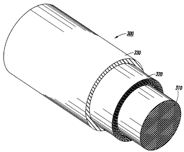
[0013] FIGS. 3A-3B depict another exemplary bias-able device including a
dual-layer structure in accordance with the present teachings.
[0014] FIG. 4 depicts an additional exemplary bias-able device including
a
triple-layer structure in accordance with the present teachings.
4
CA 02625443 2014-02-12
DESCRIPTION OF THE EMBODIMENTS
[0015] Reference will now be made in detail to the present embodiments
(exemplary embodiments) of the invention, examples of which are illustrated in
the
accompanying drawings. Wherever possible, the same reference numbers will be
used throughout the drawings to refer to the same or like parts. In the
following
description, reference is made to the accompanying drawings that form a part
thereof, and in which is shown by way of illustration specific exemplary
embodiments in which the invention may be practiced. These embodiments are
described in sufficient detail to enable those skilled in the art to practice
the
invention and it is to be understood that other embodiments may be utilized
and
that changes may be made without departing from the scope of the invention.
The following description is, therefore, merely exemplary.
[0016] While the invention has been illustrated with respect to one or
more
implementations, alterations and/or modifications can be made to the
illustrated
examples without departing from the scope of the invention. In addition, while
a
particular feature of the invention may have been disclosed with respect to
only
one of several implementations, such feature may be combined with one or more
other features of the other implementations as may be desired and advantageous
for any given or particular function. Furthermore, to the extent that the
terms
"including", "includes", "having", "has", "with", or variants thereof are used
in either
the detailed description and the claims, such terms are intended to be
inclusive in
a manner similar to the term "comprising." As used herein, the term "one or
more
of" with respect to a listing of items such as, for example, A and B, means A
alone, B alone, or A and B. The term "at least one of" is used to mean one or
more of the listed items can be selected.
CA 02625443 2008-03-13
[0017] Notwithstanding that the numerical ranges and parameters setting
forth the broad scope of the invention are approximations, the numerical
values
set forth in the specific examples are reported as precisely as possible. Any
numerical value, however, inherently contains certain errors necessarily
resulting
from the standard deviation found in their respective testing measurements.
Moreover, all ranges disclosed herein are to be understood to encompass any
and all sub-ranges subsumed therein. For example, a range of "less than 10"
can
include any and all sub-ranges between (and including) the minimum value of
zero and the maximum value of 10, that is, any and all sub-ranges having a
minimum value of equal to or greater than zero and a maximum value of equal to
or less than 10, e.g., 1 to 5.
[0018] Exemplary embodiments provide bias-able devices for use in
electrostato-graphic printing apparatuses using rubber materials, which are
mechanically conformable and electrically relaxable. In various embodiments,
the
bias-able devices can take various forms, such as, for example, rolls, films,
belts
and the like. Exemplary bias-able devices can include, but are not limited to,
bias
charging rolls (BCRs) or bias transfer rolls (BTRs), which can be subsystems
of
an electrostato-graphic printing apparatus. In various embodiments, the bias-
able
device can include a rubber material disposed over a conductive substrate such
as a conductive core depending on the specific design and/or engine
architecture.
The disclosed rubber material can include a plurality of nanotubes as filler
materials dispersed in a rubber (or polymer) matrix.
[0019] As used herein and unless otherwise specified, the term
"nanotubes"
refers to elongated materials (including organic or inorganic material) having
at
least one minor dimension, for example, width or diameter, about 100
nanometers
6
CA 02625443 2008-03-13
or less. Although the term "nanotubes" is referred to throughout the
description
herein for illustrative purposes, it is intended that the term also encompass
other
elongated structures of like dimensions including, but not limited to,
nanoshafts,
nanopillars, nanowires, nanorods, and nanoneedles and their various
functionalized and derivatized fibril forms, which include nanofibers with
exemplary forms of thread, yarn, fabrics, etc. The term "nanotubes" can also
include single wall nanotubes such as single wall carbon nanotubes (SWCNTs),
multi-wall nanotubes such as multi-wall carbon nanotubes, and their various
functionalized and derivatized fibril forms such as nanofibers. In various
embodiments, the term "nanotubes" can further include carbon nanotubes, which
can include SWCNTs and/or multi-wall carbon nanotubes.
[0020] The nanotubes can have various cross sectional shapes, such as,
for example, rectangular, square, polygonal, oval, or circular shape.
Accordingly,
the nanotubes can have, for example, a cylindrical 3-dimensional shape.
[0021] The nanotubes can be formed of conductive or semi-conductive
materials. In some embodiments, the nanotubes can be obtained in low and/or
high purity dried paper forms or can be purchased in various solutions. In
other
embodiments, the nanotubes can be available in the as-processed unpurified
condition, where a purification process can be subsequently carried out.
[0022] The nanotubes can be distributed uniformly throughout and/or
spatially-controlled throughout a rubber matrix forming a rubber material. In
some
embodiments, the nanotubes, such as carbon nanotubes, can be bundled tubes
with random tangles throughout the rubber material by a physical or chemical
bonding with desirable rubbers. In other embodiments, the nanotubes, such as
carbon nanotubes, can be spatially-controlled, for example, be aligned or
oriented
7
CA 02625443 2008-03-13
at certain directions throughout the rubber matrix by, for example, use of a
magnetic field.
[0023] In various embodiments, the rubber material can be prepared by a
physical mix and/or a chemical reaction including a biochemical reaction or
their
combination between the nanotubes and one or more rubbers. For example,
carbon nanotubes can be physically mixed and dispersed uniformly within the
rubber matrix. Alternatively, the carbon nanotubes can be covalently bonded
with
various rubbers forming the rubber material by, for example, chemical
modifications on nanotubes surfaces followed by chemical reactions between the
modified nanotubes and the rubber. In various embodiments, enzymes can be
used in biochemical reactions to provide an environmentally-friendly rubber
material for the bias-able devices. In various embodiments, a sonication
process
or other enhanced mixing process can be used during the preparation.
[0024] The rubber material can also be prepared by, for example, in-situ
processes such as an in-situ polymerization and/or an in-situ curing process
of the
rubbers of interest. For example, carbon nanotubes can be dispersed uniformly
throughout an exemplary rubber of polyimide matrix during an in-situ
polymerization of the polyimide monomers. In another example, carbon
nanotubes can be dispersed throughout an epoxy type rubber matrix during the
curing process of the epoxy.
[0025] In various embodiments, the disclosed rubber material can be used
in the bias-able devices for providing exceptional and desired functions, such
as,
mechanical and electrical functions for the devices. Specifically, the rubber
material can provide conformability, that is, being mechanically compliant and
also
strong enough for forming a nip for the bias-able devices such as BCRs. In
8
CA 02625443 2008-03-13
. ,
addition, the rubber materials can provide electrical resistivity for bias
charge of,
for example, the photoreceptors connected to BCRs. In various embodiments, the
rubber material can provide a resistivity ranging, for example, from about 105
ohm-cm to about 1010 ohm-cm, to allow charges to relax across the functional
layers while being resistive enough to avoid bias leaks at high field.
[0026] In an exemplary embodiment, the rubber material can
include
carbon nanotubes, for example, SWCNTs with a weight loading of, for example,
about 2.0 % or less to retain the mechanical property of, for example, tensile
strength and conformability of the rubber matrix.
[0027] In various embodiments, other filler materials besides
nanotubes
can be added into the rubber material. The other fillers can include one or
more
materials selected from the group consisting of carbon, graphite, Sn02, T102,
1n203, ZnO, MgO, A1203, and metal powders such as Al, Ni, Fe, Zn, or Cu.
[0028] In various embodiments, the rubber material can include a
variety of
rubbers used as a functional layer of the bias-able devices. As used herein,
the
term "rubber" refers to any elastomer (i.e., elastic material), that emulates
natural
rubber in that they stretch under tension, have a high tensile strength,
retract
rapidly, and substantially recover their original dimensions (or become even
smaller in some embodiments). The term "rubber" includes natural and man-
made (synthetic) elastomers, and the elastomers can be a thermoplastic
elastomer or a non-thermoplastic elastomer. The term "rubber" can include
blends (e.g., physical mixtures) of elastomers, as well as copolymers,
terpolymers, and multi-polymers.
[0029] Exemplary rubbers can include, but are not limited to,
ethylene-
propylene-diene monomers (EPDM), epichlorohydrin, polyurethane, silicone, and
9
CA 02625443 2008-03-13
various nitrile rubbers which can be copolymers of butadiene and acrylonitrile
such as Buna-N (also known as standard nitrile and NBR). In an additional
example, by varying the acrylonitrile content, elastomers with improved
oil/fuel
swell or with improved low-temperature performance can be achieved. Other
useful rubbers can include, but are not limited to, polyvinylchloride-nitrile
butadiene (PVC-NBR) blends, chlorinated polyethylene (CM), chlorinated
sulfonate polyethylene (CSM), aliphatic polyesters with chlorinated side
chains
such as epichlorohydrin homopolymer (CO), epichlorohydrin copolymer (ECO)
and epichlorohydrin terpolymer (GECO), polyacrylate rubbers such as ethylene-
acrylate copolymer (ACM), ethylene-acrylate terpolymers (AEM), EPR, elastomers
of ethylene and propylene which sometimes can have a third monomer such as
ethylene-propylene copolymer (EPM), ethylene vinyl acetate copolymers (EVM),
butadiene rubber (BR), polychloroprene rubber (CR), polyisoprene rubber (IR),
IM,
polynorbornenes, polysulfide rubbers (OT and EOT), polyurethanes (AU) and
(EU), silicone rubbers (MQ), vinyl silicone rubbers (VMQ), phenylmethyl
silicone
rubbers (PMQ), styrene-butadiene rubbers (SBR), copolymers of isobutylene and
isoprene known as butyl rubbers (IIR), brominated copolymers of isobutylene
and
isoprene (BIIR) and chlorinated copolymers of isobutylene and isoprene (CIIR).
[0030] In various embodiments, the bias-able devices can be used in a
"green" environment, that is, all parts, components, and materials of the
devices
can be manufactured in an "environmentally acceptable" fashion. The "green"
rubbers used in the rubber materials for the bias-able devices can include,
but are
not limited to, biocompatible rubber materials, such as, for example,
polycarboxylic acids, cellulosic polymers including cellulose acetate and
cellulose
nitrate, gelatin, polyvinylpyrrolidone including cross-linked
polyvinylpyrrolidone,
CA 02625443 2008-03-13
,
polyanhydrides including maleic anhydride polymers, polyamides, polyvinyl
alcohols, copolymers of vinyl monomers such as EVA, polyvinyl ethers,
polyvinyl
aromatics, polyethylene oxides, glycosaminoglycans, polysaccharides,
polyesters
including polyethylene terephthalate, polyacrylamides, polyethers, polyether
sulfone, polycarbonate, polyalkylenes including polypropylene, polyethylene
and
high molecular weight polyethylene, halogenated polyalkylenes including
polyurethanes, polyorthoesters, proteins, polypeptides, enzymes, silicones,
siloxane polymers, polylactic acid, polyglycolic acid, polycaprolactone,
polyhydroxybutyrate valerate, styrene-isobutylene copolymers and blends and
copolymers thereof. Other examples of the "green" rubbers can include
polyurethane, fibrin, collagen and derivatives thereof, polysaccharides such
as
celluloses, starches, dextrans, alginates and derivatives, hyaluronic acid,
squalene, etc.
[0031] Additional suitable "green" rubbers can include, thermoplastic
elastomers in general, polyolefins, polyisobutylene, ethylene-alphaolefin
copolymers, acrylic polymers and copolymers, vinyl halide polymers and
copolymers such as polyvinyl chloride, polyvinyl ethers such as polyvinyl
methyl
ether, polyvinylidene halides such as polyvinylidene fluoride and
polyvinylidene
chloride, polyacrylonitrile, polyvinyl ketones, polyvinyl aromatics such as
polystyrene, polyvinyl esters such as polyvinyl acetate, copolymers of vinyl
monomers, copolymers of vinyl monomers and olefins such as ethylene-methyl
methacrylate copolymers, acrylonitrile-styrene copolymers, ABS (acrylonitrile-
butadiene-styrene) resins, ethylene-vinyl acetate copolymers, polyamides such
as
Nylon 66 and polycaprolactone, alkyd resins, polycarbonates,
polyoxymethylenes,
polyimides, epoxy resins, rayon-triacetate, cellulose, cellulose acetate,
cellulose
11
CA 02625443 2008-03-13
butyrate, cellulose acetate butyrate, cellophane, cellulose nitrate, cellulose
propionate, cellulose ethers, carboxymethyl cellulose, collagens, chitins,
polylactic
acid, polyglycolic acid, polylactic acid-polyethylene oxide copolymers, EPDM
(etylene-propylene-diene) rubbers, polyethylene glycol, polysaccharides,
phospholipids, and combinations of the foregoing.
[0032] In various embodiments, rubbers can be obtained from chemical
modifications (e.g., derivatives), and be used in rubber materials to provide
additional functions and/or to improve the performance of the bias-able
devices.
For example, a polyurethane can be a modified polyurethane obtained by varying
the structure of the monomers in the pre-polymer; a polyolefin can be a
modified
polyolefin including copolymers of polyolefins or blends; and a
epichlorohydrin can
be a modified epichlorohydrin copolymerized with varying amount of ethylene
oxide.
[0033] In various embodiments, the rubber material can further include a
variety of additives, such as, for example, plasticizers, softening agents,
dispersant aid, and/or compatiblizer, which can be added to render the rubber
materials with desired useful properties known to one of the ordinary skill in
the
art.
[0034] In various embodiments, the disclosed bias-able device can include
a conductive substrate, that can be formed in various shapes and using any
suitable material for bias charging. For example, the conductive substrate can
take the form of a cylindrical tube or a solid cylindrical shaft of, for
example,
stainless steel, aluminum, copper, or certain plastic materials chosen to
maintain
rigidity, structural integrity and be capable of readily responding to a
biasing
12
CA 02625443 2008-03-13
potential placed thereon. For example, the conductive substrate can be a solid
cylindrical shaft of stainless steel.
[0035] Generally, the bias of the bias-able device can be controlled by
use
of a DC potential. An AC potential can also be used along with the DC
controlling
potential to aid the charging control. In various embodiments, the bias-able
device can be used as BCRs and/or BTRs. The basic construction and operating
principal for these two exemplary types of rolls can be similar. For example,
in the
case of BCRs, an electric field can be created above the air-breakdown limit
(i.e.,
Paschen field limit) in the pre-nip and post-nip regions when the BCRs are
loaded
against photoreceptor drums. When the field exceeds the Paschen limit, it can
break the air down generating a corona current that can charge the
photoreceptor.
In the case of BTRs, an electric field can be created without breaking down
the
air. This electric field can then aid the transfer of the toner images from
the
photoreceptor to the printing substrate.
[0036] In various embodiments, the disclosed bias-able device can also
include one or more rubber materials disposed upon the conductive substrate
and/or other functional layers of the device. In some embodiments, the rubber
material can be, for example, coated or cast on the underlying surface, for
example, surfaces of the conductive substrate or the other functional layers.
In
other embodiments, the rubber material can be, for example, extruded or molded
to be accommodated with the configurations of the disclosed device.
[0037] In various embodiments, the disclosed bias-able device can further
include a surface material as an outer layer, for example, a surface
protecting
and/or resistivity adjusting layer, known to one of ordinary skill in the art.
The
surface layer (i.e., the outer layer) of the bias-able device can be used to
protect
13
CA 02625443 2008-03-13
the inside layers from abrasion and toner contamination. The surface layer can
have a thickness of about 0.01 mm to about 0.1 mm. In various embodiments, the
surface layer can be prepared using a variety of polymers or rubbers
including,
but not limited to, nylons, polyurethanes such as fluorinated polyurethane,
fluoropolymers, polyesters, polycarbonates, acrylic acid resins, different
kind of
celluloses, phenoxy resin, polysulfone, and polyvinylbutyral. In various
embodiments, the surface layer can further include conductive fillers, such
as, for
example, Sn02, Ti02, carbon, and fluorinated carbon. In an exemplary
embodiment, polymers with low surface energy, such as polymers containing
fluorinated fillers, can be used in the surface material to reduce toner
contamination.
[0038] Exemplary bias-able devices can have one or more functional layers
provided upon a conductive substrate as shown in FIGS. 1A-1B, FIGS. 3A-3B and
FIG. 4 in accordance with the present teachings. The rubber material can be
used as one of the one or more functional layers to provide uniform mechanical
and electrical functions.
[0039] FIGS. 1A-1B depict an exemplary bias-able device 100 including a
single-layer structure disposed upon a conductive substrate in accordance with
the present teachings. In particular, FIG. 1A is a perspective view of a
partial
section of the exemplary bias-able device 100, while FIG. 1B is a cross-
sectional
view of the exemplary bias-able device 100 shown in FIG. 1A. It should be
readily
apparent to one of ordinary skill in the art that the device depicted in FIGS.
1A-1B
represents a generalized schematic illustration and that other
layers/materials can
be added or existing layers/materials can be removed or modified.
14
CA 02625443 2008-03-13
. .
[0040] As shown in FIGS. 1A-1B, the exemplary bias-able device
100 can
include a conductive substrate 110, and a rubber material 120. The rubber
material 120 can be disposed on the conductive substrate 110. The rubber
material 120 can include, for example, a plurality of nanotubes 125
distributed
throughout a rubber matrix 128.
[0041] The conductive substrate 110 can be any conductive
substrate as
described herein. The size of the conductive substrate 110 can depend on the
compliance of the rubber material, and more importantly, the size of the
printing
machine and the speed of the operation. For example, the conductive substrate
110 can be a solid cylindrical shaft of stainless steel having a diameter of
the
cylindrical tube of about lmm to about 15 mm, and a length of about 10 mm to
about 500 mm. In an additional example, the diameter of the conductive
substrate
110 can be about 6 mm to about 15 mm and the length can be about 200 mm to
about 500 mm. In a further example, the diameter of the conductive substrate
110
can be less than about 6 mm and the length can be less than about 200 mm.
[0042] The rubber material 120 can be disposed upon the surface
of the
conductive substrate 110. The rubber material 120 can be a conductive elastic
layer configured to be responsible for the conformability (i.e., compliance)
and the
resistivity, which can be relative to the process speed and/or the AC
frequency in
the case of AC/DC condition. That is, the rubber material 120 can provide the
nip-
forming function and also relax the charge across the layer.
[0043] The rubber material 120 can be prepared including one or
more
rubbers and a plurality of nanotubes as disclosed herein. For example, the
rubber
material 120 can include a plurality of nanotubes 125 dispersed throughout a
rubber matrix 128 as illustrated in FIG. 1A-1B. In this example, the plurality
of
CA 02625443 2008-03-13
. ,
nanotubes 125 can be oriented in a certain direction throughout the polymer
matrix 128 for a desirable function. In various embodiments, a plurality of
carbon
nanotubes such as SWCNTs can be dispersed physically or chemically
throughout various rubber materials such as, for example, epichlorohydrins,
urethanes, EPDM (ethylene propylene diene monomers), styrene-butadienes,
silicones, chloroprenes, butyl rubbers, isoprenes, polyester thermoplastic
rubbers,
natural rubbers and the like.
[0044] In various embodiments, the rubber material 120,
including a
plurality of nanotubes within a rubber matrix can be, for example, coated or
cast
on surface of the conductive substrate 110. In various other embodiments, the
rubber material 120 can be, for example, extruded or molded to be
accommodated with the configurations of the conductive substrate 110.
[0045] In an exemplary embodiment, the rubber material 120 can
include
rubbers that can be dissolved and cured or polymerized in situ on the surface
of
the conductive substrate 110 of the bias-able device 100. In another exemplary
embodiment, the rubber material 120 can include rubbers having relatively low
melting points, which can be blended with biologically active materials and
coated
on the conductive substrate 110. In an additional embodiment, the rubber
material 120 can include biocompatible materials, enzymes and/or their
biochemical reactions.
[0046] In various embodiments, the rubber material 120 can
provide a
desired resistivity, for example, ranging from about 105 ohm-cm to 1010 ohm-
cm.
This resistivity range can be achieved with a low carbon-nanotube-loading such
that the filler effect on compliance and other mechanical properties of the
rubber
used can be minimal and thus providing a wide material selection latitude.
This is
16
CA 02625443 2011-09-20
also because the electrical percolation of the rubber material 120 can be
achieved
by a very low carbon-nanotube-loading, for example, about 0.05 % by weight. In
an exemplary embodiment, the carbon nanotube loading of the rubber material
120 can be about 2% by weight or less.
[0047] FIG. 2 depicts an exemplary electrical result of a rubber material
containing SWCNTs in accordance with the present teachings. As shown, when
there is no loading of SWCNTs, the conductivity of the exemplary material can
be
about 10-17 S/CM (1017 ohm-cm). The conductivity of the material can be
controlled by adding SWCNTs as conductive fillers to the rubber material. For
example, when the loading levels of SWCNTs are in excess of about 0.1 wt.%,
the
conductivity of the rubber material can be about 10-8 s/cm (108 ohm-cm), which
can be a desired conductivity/ resistivity for the rubber material 120.
Various
conductivities/ resistivities or ranges of conductivity/ resistivity can be
obtained
and determined by the loading levels of the nanotubes (as indicated in FIG. 2)
and/or the type of rubbers used.
[0048] In various embodiments, other functional layers can be added over
the conductive substrate to meet, for example, the abrasion requirement, which
can result in dual-, triple-, quad- or multiple-layered bias-able devices. The
functional layers including the rubber material can provide desired
mechanical,
electrical, and surface functions for the bias-able devices in a manner that
each of
these functions can be separated and/or arbitrary combined in the discrete
functional layers. For example, the functional layers can include, but are not
limited to, a compliant layer, a conductive elastic layer (e.g., the rubber
material),
an electrode layer, a resistance adjusting layer, a surface protecting layer,
or any
other functional layer.
17
CA 02625443 2008-03-13
, .
[0049] FIGS. 3A-3B depict an exemplary bias-able device 300
having a
dual-layer structure coated upon a conductive substrate in accordance with the
present teachings. In particular, FIG. 3A is a perspective view in partial
section of
the exemplary bias-able device 300. FIG. 3B is a cross-sectional view of the
exemplary bias-able device 300 shown in FIG. 3A. It should be readily apparent
to one of ordinary skill in the art that the devices depicted in FIGS. 3A-3B
represent a generalized schematic illustration and that other layers/materials
can
be added or existing layers/materials can be removed or modified.
[0050] As shown in FIGS. 3A-3B, the exemplary bias-able device
300 can
include a conductive substrate 310, a rubber material 320, and a surface
material
330. The surface material 330 can be a surface resistive/protecting layer
disposed on the rubber material 320 forming a dual-layer structure formed on
the
surface of the conductive substrate 310. In various embodiments, the device
300
can be formed by simply disposing a surface layer on the rubber material 220
of
the device 200.
[0051] The conductive substrate 310 can use a substrate that is
similar to
the conductive substrate 110 as described in FIGS. 1A-1B. The rubber material
320 can be any rubber material as disclosed herein disposed upon the surface
of
the conductive substrate 310 to provide uniform mechanical and electrical
properties for the bias-able device 300. The rubber material 320 can be
prepared
including a plurality of carbon nanotubes distributed within a rubber matrix.
In an
exemplary embodiment, the rubber materials 320 can include SWCNTs dispersed
uniformly throughout rubber matrices including, but not limited to, EPDM
(ethylene
propylene diene monomers), epichlorohydrins, urethanes, styrene-butadienes,
silicones, chloroprenes, butyl rubbers, isoprenes, polyester thermoplastic
rubbers,
18
CA 02625443 2008-03-13
, .
natural rubbers and the like. In various embodiments, the rubber material 320
can
include a plurality of SWCNTs with an exemplary weight loading of, for
example,
about 2.0% or less. In an additional example, the weight loading of SWCNTs can
be about 0.1% or less.
[0052] The surface material 330 can be disposed on the rubber
material
320. The surface material 330 can be any surface material configured as a
surface protecting layer and/or a resistivity adjusting layer known to one of
ordinary skill in the art. In various embodiments, the resistance of the
surface
material 330 can dominate the resistance of the bias-able devices 300, for
example, a BCR, to reduce the electrical environmental instability of the
entire
BCR.
[0053] In various embodiments, the exemplary dual-layer bias-able
device
300 can be used in both BCR and BTR applications. Generally, in a color
machine of an electrostato-graphic printing apparatus, there can be a BCR
configured to charge the photoreceptor, and there can be at least two BTRs
configured in the color machine. For example, there can be two BTRs for the 4-
cycle color engine and there can be five BTRs for a 4-color tandem engine. In
the
4-cycle color engine, the first BTR can be configured at the nip interface of
the
photoreceptor and intermediate transfer belt, and the second BTR can be
configured at the interface of intermediate transfer belt and, for example,
paper.
Depending on the application and/or the architecture of the BCRs and BTRs, the
electrical requirement of these devices can be different. In addition, the
dimensions (e.g., diameter, and/or thickness) of each material of the
conductive
substrate 310, the rubber material 320 and the surface material 330 can also
depend on the machine architecture and the intended operating speed.
19
CA 02625443 2008-03-13
. .
[0054] According to various embodiments when the bias-able
device 300 is
used for a BCR application, the rubber material 320 can have a thickness of
about
1-3 mm and provide a resistivity ranging from about 104 ohm-cm to about 108
ohm-cm at the operating field. The surface material 330 can have a thickness
of
about 0.01-0.1 mm and provide a resistivity of about 107 ohm-cm to about 1011
ohm-cm.
[0055] According to various embodiments when the bias-able
device 300 is
used for an application of the first BTR of the 4-cycle color engine, the
rubber
material 320 can have a thickness of about 3-5 mm and provide a resistivity
ranging from about 105 ohm-cm to about 1010 ohm-cm at the operating field. The
surface material 330 can have a thickness of about 0.01-0.1 mm and provide a
resistivity of about 108 to about 1012 ohm-cm. In this case, the conductive
substrate 310 can be, for example, a stainless steel shaft, and can have a
diameter of about 8-12 mm.
[0056] FIG. 4 depicts an exemplary bias-able device 400 having a
triple-
layer structure disposed upon a conductive substrate in accordance with the
present teachings. In particular, FIG. 4 is a cross-sectional view of the
exemplary
bias-able device 400. It should be readily apparent to one of ordinary skill
in the
art that the devices depicted in FIG. 4 represents a generalized schematic
illustration and that other layers/materials can be added or existing
layers/materials can be removed or modified.
[0057] As shown in FIG. 4, the exemplary bias-able device 400
can include
a conductive substrate 410, a conductive foam 415, a rubber material 420, and
a
surface material 430. The surface material 430 can be an outer layer disposed
on
CA 02625443 2008-03-13
. .
the rubber material 420 disposed on the conductive foam 415 and form a triple-
layer structure disposed on the surface of the conductive substrate 410.
[0058] The conductive substrate 410 can be a substrate that is
similar to
the conductive substrate 110 and/or the conductive substrate 310 as described
in
FIGS. 1A-1B and/or FIG. 3. In various embodiments, the conductive substrate
410 can be, for example, a stainless steel shaft.
[0059] The conductive foam 415 can be, for example, a conductive
polyurethane foam to provide additional compliance for the device 400. The
conductive foam 415 can be formed by, for example, molding the foam material
according to the configuration of the conductive substrate 410.
[0060] The rubber material 420 can be any disclosed rubber
material
disposed upon the surface of the conductive foam 415. The rubber material 420
can be similar to the rubber material 120 and/or 320 as described in FIGS. 1
and/or FIG. 3 to provide uniform mechanical and electrical properties for the
bias-
able device 400.
[0061] The surface material 430 can be disposed on the rubber
material
420. The surface material 430 can be any surface material configured as a
surface protecting and/or resistivity adjusting layer known to one of ordinary
skill in
the art.
[0062] In various embodiments, the device 400 can have a large
size for
each layer and can be more compliant. For example, the bias-able device 400
can be used for an application of the second BTR for the exemplary 4-cycle
color
engine. In this example, the conductive substrate 410 can be, for example, a
stainless steel shaft, and can have a diameter of about 10 mm to about 15 mm.
The conductive foam 415 can have a thickness of, for example, about 3 mm to
21
CA 02625443 2013-01-29
about 5 mm. The rubber material 420 can have a thickness of about 3 mm to
about 5 mm.
[0063] Other
embodiments of the invention will be apparent to those skilled
in the art from consideration of the specification and practice of the
invention
disclosed herein. It is intended that the specification and examples be
considered
as exemplary only, with a true scope of the invention being indicated by the
following claims.
22