Note: Descriptions are shown in the official language in which they were submitted.
CA 02625635 2008-04-10
WO 2007/055625 PCT/SE2005/001713
TITLE: COOLING ASSEMBLY
TECHNICAL FIELD
The present invention generally concerns the cooling of heat generating
electronic applications
by means of heat sinks brought into heat transferring thermal contact with a
printed circuit
board (PCB) mounted heat generating component of the application.
BACKGROUND
Present day electronic applications commonly include PCB mounted components,
such as chips or
microprocessors, that generate much heat and that are also very sensitive to
overheating and
therefore require optinium cooling to be maintained at acceptable operating
temperatures. One
important prerequisite for acliieving effective cooling is to optimize thermal
contact between the
component and the heat sink by minimiziuig thermal resistance of the joint
between the-heat
transfer contact surfaces of the heat sink and the component. This is
generally achieved with good
surface structure and measurement precision and parallelism between the
component and heat
sinks surfaces. In theory, acceptable thermal resistance values would be
achievable by securing
flatness of as well as parallelism between the surfaces and by producing high
surface finish for
both surfaces. In practice, however, it would be far too expensive to produce
a surface finish that
would sufficiently reduce the interstitial air caught in gaps formed between
the contact points of
even polished surfaces.
Although good surface structure can be achieved by machining, e.g. of the
commonly used
aluminum heat sink, it is also a fact that in practical applications
parallelism between the contact
surfaces and height of the component surface above a PCB is often not very
exact, being dependent
on i.a. soldering joints. For the above reasons, it is common practice to
improve the thermal contact
by providing thermal interface material, such as thermal grease, thermal tape,
thermal phase
change material and various thermally conductive gap filler materials, between
the contact surfaces
to fill the microscopic gaps formed by the roughness of the surfaces and to
thereby increase the
heat transfer from the component to the heat sink. However, gap filler or
other thermal interface
material shall not be used to fill "large gaps" since the conductivity is not
good enough. A gap-filler
shall likewise not be used to compensate for dynamic changes of the gaps,
caused e.g. by shock or
vibration.
CA 02625635 2008-04-10
WO 2007/055625 PCT/SE2005/001713
2
Thermal contact between heat sink and component is dependent also on the
contact pressure,
and in this context higher contact pressure means smaller gaps and hence
better contact.
Resilient clamp and/or spring attachments are therefore often used to hold
together component
and heat sink and to provide appropriate contact pressure for ensuring
intimate thermal contact
between the contact surfaces, without putting excessive load on either
component or printed
circuit board.
One problem associated with today's cooling assemblies for heat generating
electronic
applications is that the integrity of the thermal interface between the
component and the heat
sink may become disturbed or even destroyed both during transport of the
application and
during its operation. A cause of such problems is the dynamic dimensional
changes that may
occur in different environments, such as by differential thermal
expansion/contraction or by
changes in air humidity affecting plastic materials. Such problems may also
occur if an
application is subjected to mechanical shock during transport, in its normal
operational
environment, by accident or even caused by natural forces, such as assemblies
operating in
areas subjected to eartllquakes. The problem is quite obviously aggravated in
applications
having small size highly heat generating components that for their cooling
require
comparatively large and heavy heat sinks. Due to the great mass of the heat
sink and its large
extension past the component contact surface, even moderate shock may destroy
the intimate
contact between the component and the heat sink and thereby be detrimental to
the thermal
interface there between.
SUMMARY
It is a general object of the present invention to provide effective and
reliable cooling of
applications of electronic equipment having heat generating components.
In particular, a basic object of the invention is to suggest a principle of
electronic equipment
cooling, providing long-time stable cooling with essentially maintained
thermal resistaiice in
the thermal interface between a component and a heat sink.
It is a specific object of the invention to provide an improved method of long
time stable cooling
of heat generating electronic component applications on a circuit board by
means of a cooling
CA 02625635 2008-04-10
WO 2007/055625 PCT/SE2005/001713
3
assembly including a heat sink attached to the circuit board in heat
transferring thermal contact
with a heat generating electronic component and to provide an electronic
application employing
such iunproved cooling principles.
Another specific object of the invention is to provide an improved cooling
assembly for long
time stable cooling of heat generating electronic component applications on a
circuit board,
including a heat sink attached to the circuit board in heat transferring
thermal contact with a
heat-generating electronic component.
Another specific object of the invention is to provide an improved method of
long time stable
mounting of a cooling assembly to a printed circuit board for cooling heat
generating electronic
coinponent applications on the PCB by means of a heat sink attached in heat
transferring, thermal
contact with a heat generating electronic component.
These and other objects are met by the invention as defined by the
accompanying patent claims.
The invention concerns the removal of heat from a heat generating electronic
component mounted
on a PCB, by means of a heat sink attached to the PCB in thermal contact with
said component. It
has been recognized that the above objects are achieved by securing a
controlled and uniform
pressure between heat sink and heat generating component. A basic idea is to
secure the heat sink
to the PCB in a stationary position, at a fixed distance from said circuit
board and to resiliently bias
the component against -the heat sink. This will provide inherent automatic
compensation for
dynamic dimensional changes as well as assembly tolerances and manufacturing
tolerances of
parts of the equipment by employing the resilience of the substrate of the
PCB.
In accordance with a further aspect of the invention improved optimized
cooling may also be
achieved for applications having several further, closely mounted components.
A basic idea of
this aspect of the invention is to provide one separate heat sinlc for each of
said further
components and to use the heat sink of the main heat generating component to
resiliently force
said additional heat sinks against the further components. With this design,
tolerance conflicts
of the components may be avoided and individual optimization of the heat sinks
for each
component may be obtained.
CA 02625635 2008-04-10
WO 2007/055625 PCT/SE2005/001713
4
By securing the heat sink to the PCB at discrete positions in an outer area of
the heat sink, the
attachment has a negligible affect on the total flow of cooling air between
the heat sink and the
PCB, so that effective cooling may be achieved also for other components that
are not in direct
heat transfer contact with a main heat sink.
Preferably, the heat sink is secured to the PCB in an outer peripheral area
thereof and the
biasing force is applied closely outside the component. This solution provides
for a significant
distance between the area where the heat sink is secured to the PCB and the
area where the
biasing force is applied, so that the flexibility of the PCB substrate may be
effectively employed
for tolerance and heat expansion compensation. Such a solution is also
excellent for applications
having a heat generating component requiring a very large and accordingly
heavy heat sink.
In one embodiment that provides specifically good conditions for providing a
controlled flexing of
the PCB substrate to compensate for existing tolerances and thereby ensure low
thermal resistance
of the thermal interface, the biasing forces are applied through a backing
frame that underlies and
stabilizes the PCB substrate in the area of the component.
The specified height of the heat sink above the PCB is defined for each
application in relation to a
nominal height of the mounted heat generating component above the PCB, and is
preferably
chosen to be approximately equal to such a nominal height.
In other embodiments the specified height of the heat sink above the PCB is
determined by
means of standoffs of specified length being provided between the PCB and the
heat sink and
being formed integral with or separate from the heat sink.
A cooling principle according to the present invention offers a number of
advantages, including:
- Compensates for variations due to mechanical tolerances, heat expansion etc.
in heat sink,
component holder, component, PBC and solder joints;
- Enables the application of controlled and uniform contact pressure even
between a large
and heavy heat sink and a comparatively small component; and thereby
CA 02625635 2008-04-10
WO 2007/055625 PCT/SE2005/001713
- Allows for establishing good thermal contact between heat sink and
component;
- Permits individual optimization of the heat sink for each component.
5 - The fastening arrangement occupies minimum board space;
- Low and predictable thermal resistance between the heat sink and the
component, with
low variations between individual boards;
- Mechanically robust, thereby meeting mechanical strength and endurance
requirements
with regard to vibration and shock (e.g. by transportation, office vibration
or earthquake);
Advantages offered by the present invention, in addition to those described
above, will be readily
appreciated upon reading the below detailed description of embodiments of the
invention.
BRIEF DESCRIPTION OF THE DRAWINGS
The invention, together with further objects and advantages thereof, will be
best understood by
reference to the following description taken together with the accompanying
drawings, in which:
Fig. 1 is an exploded isometric view from above of a first embodiment of a
cooling assembly
for an electronic application, according to the invention;
Fig. 2A is a partly schematical side view of a first practical example of a
cooling assembly of
the first embodiment mounted to the electronic application of Fig. 1;
Fig. 2B is a likewise partly schematical top view of the installation of Fig.
2A;
Fig. 3A is a schematical illustration that, greatly exaggerated, exemplifies a
tilted component
on a PCB of a variant of the electronic application of Fig. 2A-B, before
mounting of
the cooling assembly;
Fig. 3B is a schematical illustration, in a section taken along line A-A in
Fig. 2B, that, likewise
greatly exaggerated, illustrates a second practical example of the cooling
assembly of
the first embodiment mounted to the schematical electronic application of Fig.
3A;
CA 02625635 2008-04-10
WO 2007/055625 PCT/SE2005/001713
6
Fig. 4A is a schematical side view that, greatly exaggerated, exemplifies a
component mounted
at reduced height on a PCB of a further variant of the electronic application
of Fig. 2A-
B, before installing the cooling assembly;
Fig. 4B is a side view that, likewise greatly exaggerated, illustrates a third
practical example of
the cooling assembly of the first embodiment mounted to the schematical
electronic
application of Fig. 4A;
Fig. 5A is a partly schematical side view of a second embodiment of a cooling
assembly
mounted to an alternative electronic application, according to the invention,
Fig. 5B is a likewise partly schematical top view of the assembly of Fig. 4A;
Figs. 6 is a schematical illustration, in a section taken along line B-B in
Fig. 5B; that,
greatly exaggerated, exemplifies a practical example of the cooling assembly
of the
second embodiment mounted to the electronic application of Fig. 5A, having a
tilted
component mounted on a PCB.
DETAILED DESCRIPTION
The invention will now be explained with reference to embodiments that are
illustrated in the
accompanying drawing figures and that exeinplify the use of the inventive
cooling principles in
electronic applications that include a cooling assembly attached to electronic
equipinent. A first
exemplifying embodiment of the invention is illustrated in Figs. 1 and 2A-B
and relates to an
electronic application 1 including a partially and very schematically outlined
printed circuit board
(PCB) on which is mounted a likewise schematically outlined electronic
component 3 in the form
of a processor or other highly heat generating component. It shall be
emphasized, though that the
illustrations are for the purpose of describing preferred embodiments of the
invention and are
not intended to limit the invention to the details thereof.
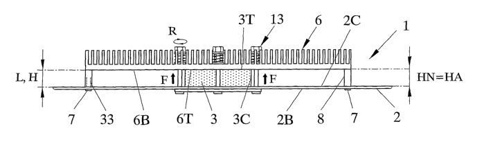
In this application 1, heat generated by the electronic component 3 is removed
from the component
3 by means of a cooling assembly primarily consisting of a rigid heat sink 6
that is attached to the
PCB 2 in heat transferring thermal contact with the heat generating electronic
component 3 and
from which heat is transferred away from the application 1 in an appropriate,
not specifically
CA 02625635 2008-04-10
WO 2007/055625 PCT/SE2005/001713
7
illustrated manner, such as by means of forced air flow, heat pipes etc. A
distinctive feature of
the invention is that in the assembled application 1, outer areas of the heat
sink 6 are secured
to the circuit board 2 so that the heat sink 6 is held in a static or
stationary position relative to
the PCB and at a specified height L (see Figs 2A and 3B) above the printed
circuit board 2. In
particular, in the illustrated embodiment, the heat sink 6 is fixed to the
circuit board 2 at discrete
first positions 9-12 (see Fig. 2B) in the outer area of the heat sink,
preferably in an outer
peripheral area of the heat sink 6 with regard to its extension in a direction
parallel to the circuit
board 2, or expressed otherwise, close to the outer circumference 6C of the
heat sink 6. The
number of fixing positions 9-12 is four in the illustrated embodiment, but may
be varied
dependent upon the shape, size and/or weight of the heat sink used in each
application. In any
case, the number of and distribution of the first fixing positions 9-12 around
the periphery of the
heat sink 6 shall be sufficient to statically fix the heat sink in all
directions relative to the PCB.
To serve the purposes of the invention, the heat sink 6 is rigid or stiff
compared to the PCB
substrate and with respect to the later discussed forces that are used to
apply the required
contact pressure between the heat sink 6 and the coinponent 3. The heat sink 6
may preferably
be made e.g. of extruded aluminum.
The heat sink 6 is fixed relative to the circuit board 2 with a lower thermal
contact surface 6T (Fig.
2A) thereof being provided at a specified distance H above the level of the
circuit board 2 at said
first positions 9-12. Specifically, the heat sink 6 is positively fixed to the
printed circuit board 2 by
means of first attachments 7 that are here schematically illustrated as screw
or bolt type fasteners.
From the underside 2B of the PCB 2, with regard to the mounting of the
component 3 thereon, said
first attachments 7 are introduced through corresponding holes 32 in the PCB 2
and into engage-
ment with threaded bores 33 (outlined in Fig. 1) formed in lower ends of
standoffs 8 of specified
length L, being provided between an upper surface 2C of the PCB 2 and a lower
surface 6B of the
heat sink 6 at the first positions 9-12. In the illustrated embodiment the
standoffs 8 are formed
integral with the heat sink 6, at each corner area of the generally
rectangular heat sink 6.
The length L of these standoffs 8 determines the height of the secured heat
sink 6 above the circuit
board 2 at said first positions 9-12 and in the illustrated embodiment where
the lower thermal
contact surface 6T is at a level with a lower surface 6B of the heat sink 6
said heights L and H are
CA 02625635 2008-04-10
WO 2007/055625 PCT/SE2005/001713
8
equal. In variants of the heat sink, not illustrated, the thermal contact
surface 6T may, however, be
positioned at a different level, separated from the lower surface 6B of the
actual heat sink 6, so
that said heights L and H, respectively, differ. The length L of the standoffs
8 is chosen in relation
to a nominal height HN (see Fig. 2A) of a thermal contact surface 3T of the
mounted component
3 above the circuit board 2, and in the applicable case in relation to the
relative positioning of the
lower heat sink surface 6B and the thennal contact surface 6T, so that the
height H of the thermal
contact surface 6T is approximately equal to the nominal height HN of the
component 3, for
reasons that will be described further below. The associated thermal contact
surfaces 6T, 3T of the
heat sink 6 and the coinponent 3, respectively, each have a substantial area
permitting effective
heat transfer from component 3 to heat sink 6. Said surfaces are preferably
completely flat, as
illustrated, but may alternatively have other complementary shapes allowing
for an intimate
parallel contact, such as concave and convex arcs of the same radius.
Furthermore, in accordance with the invention, the heat sink 6 is resiliently
connected to the
circuit board 2 through biasing forces F (see Figs. 3B and 4B) applied between
the heat siuik 6 and
the printed circuit board 2, with the heat sink 6 acting as a fixed anvil due
to the fixed attachment
thereof to the PCB at said first positions 9-12. The biasing forces F are
applied to the PCB 2 in an
area outside the heat generating component 3, preferably closely surrounding
the component 3.
Specifically, in the illustrated embodiment, the heat sink 6 is attached to
the PCB 2 through a
second attachment 13 resiliently connecting the heat sink 6 to the circuit
board 2 at discrete second
positions 21-24 just outside an outer circutnference 3C (Fig. 2A) of the
component 3.
Said second attachment 13 comprises a backing frame 15 that is provided on the
underside 2B of
the substrate of the PCB 2, i.e. on the opposite side of the circuit board 2
from the component 3,
and aligned with the component. In order to lower the weight of the frame 16
it is preferably
provided with a central cut-out 17 underlying the central area of the
component 3. The backing
frame carries a nutnber of, in the illustrated embodiment four, bolt-like
fasteners 16 extending
upwardly therefrom and in the assembled condition being extended through
associated apertures
formed in the circuit board 2. Preferably, said circuit board apertures 30 are
evenly distributed
30 around the outer circumference 3C of the heat generating component 3, and
they are provided at
locations corresponding to said second positions 21-24. The fasteners 16
extend further upwardly,
CA 02625635 2008-04-10
WO 2007/055625 PCT/SE2005/001713
9
through heat sink apertures 31 that in the assembled condition are aligned
with the circuit board
apertures 30 at said second positions 21-24.
At their portion protruding from the upper side of the heat sink 6, the
fasteners 16 each carry
an intermediary biasing means 14, here in the shape of a coil spring that on
both sides is
flanked by a washer 19 and 20, respectively. The distal end of the fasteners
16 carries a nut
member 18 that during assembly will be tightened into indirect engagement,
through the
biasing means 14, with the heat sink 6 to apply the resilient biasing forces F
to the circuit
board 2 in the area of said component 3. The biasing means 14 and the nut
members 18 are in
their assembled condition accommodated in cut-outs 34-37 formed in the upper
finned surface
6A of the heat siuik 6. As will be described more closely below, the biasing
forces F will be
employed to secure the desired unifornn contact and the required contact
pressure between the
thermal contact surfaces 6T, 3T of the heat sink 6 and the component 3,
respectively.
Mounting of the cooling assembly 6-8 and 13 to the printed circuit board 2
will now be described.
To secure the heat sink 6 to the circuit board 2 at the first positions 9-12,
the heat sink 6 is first laid
upside down so that the lower surface 6B thereof faces upwardly. The printed
circuit board 2 is
then positioned on the heat sink 6 with the mounted component 3 facing the
lower surface 6B of
the heat sink 6 and with the heat transfer contact surface 3T of the component
3 aligned with the
thermal contact surface 6T of the heat sink 6. At said first positions 9-12,
the first attachments 7 are
extended through the apertures 32 in the circuit board 2, and are brought into
engagement with the
bores 33 of the standoffs 8. The first attachments 7 are then tightened to fix
the heat sink 6 to the
circuit board 2 in the stationary position with its lower thermal contact
surface 6T being provided
at the specified distance L, H from the circuit board 2 at said first
positions 9-12. Depending upon
the mechanical tolerances and especially upon the mounted position of the
component 3 this
tightening of the first atta.chments 7 to fix the heat sink 6 to the PCB 2,
may result in a local elastic
deformation of the PCB substrate or may leave a small gap between heat sink 6
and component 3,
as will be described further below. However, reference is first made to Fig.
2A that illustrates an
ideal case where the actual height HA of the contact surface 3T of the mounted
component 3 above
the PCB 2 is approximately equal to the nominal height HN and where there is
parallelism between
the contact surfaces 6T, 3T. In this case tightening of the first attachments
7 will bring the thermal
contact surfaces 6T, 3T into intimate contact with each other, preferably
through a gap filler
CA 02625635 2008-04-10
WO 2007/055625 PCT/SE2005/001713
material (not specifically shown) pre-applied to the component contact surface
3T, but without any
significant elastic deformation of the PCB substrate.
With the heat sink 6 fixed to the PCB 2, the second attachment 13 is fitted at
said second positions
5 21-24 by extending the bolt-like fasteners 16 through the circuit board
apertures 30 until the
backing frame 15 engages the underside 2B of the PCB 2. The whole application
1 is then turned
over 180 and the biasing means 14 are placed over the free ends of the
fasteners 16 that are
extended through the apertures 31 and cut-outs 34-37 of the heat sink 6.
Finally, the nuts 18 are
brought into engagement with the fasteners 16 and are tightened with a
specified torque R to
10 establish the correct contact pressure between the heat sink 6 and the
component 3.
A different practical situation is illustrated in Figs 3A-B. In this case the
component 3 has
been mounted with a tilt caused e.g. by improperly formed solder joints 2A and
resulting in an
actual maximum height HA1 of the component 3 that clearly exceeds the nominal
height NH.
It must be clarified though, that the tilt and height difference have been
heavily exaggerated in
Figs. 3A-B (as well as in the later discussed Figs 4A-B and 6) and in practice
amount to only
fractions of the illustrated measurements.
In this case, Fig. 3A briefly illustrates the situation before tightening of
the first attachments 7,
namely the lack of parallelisin between the contact surfaces 6T and 3T and the
difference in
height. The forces that are then applied through the first attachments 7 will
in this situation
cause downwardly directed flexing of the PCB substrate to accommodate the
difference in
height and lack of parallelism between the contact surfaces 6T, 3T of the heat
sink 6 and the
component 3, respectively, as is schematically illustrated in Fig. 3B. The
flexing of the PCB
effectively compensates for the tilt and height variations, partly due to the
relatively large distance
between the first and second positions 9-12 and 21-24, respectively. With the
invention, the
resiliency of the PCB 2 substrate will thus be employed to provide effective
inherent and automatic
compensation not only for assembly tolerances and manufacturing tolerances of
parts of the
equipment but also for dynamic dimensional changes during transport and
operation of the
application. The tightening of the second attachment 13, through the support
of the backing frame
15, then provides the required resilient force F for achieving a controlled
contact pressure between
the heat sink 6 and component 3 surfaces 6T and 3T, respectively.
CA 02625635 2008-04-10
WO 2007/055625 PCT/SE2005/001713
11
A further practical situation when using the invention is illustrated in Figs.
4A-B, where the actual
height HA2 of the component contact surface 3T is smaller than the nominal
height HN. Fig. 4A
briefly illustrates the situation after tightening the first attachments 7. A
small gap still exists
between the contact surface 6T of the secured heat sink 6 and the component
contact surface 3T. In
this case, the resilient force F applied by tightening the second attachment
13 will, likewise through
the support of the backing frame 15, first close the small gap between heat
sink 6 and component 3
by upwardly directed elastic deformation of the PCB substrate, and will then
provide the controlled
uniform contact pressure between the heat sink and component surfaces 6T and
3T.
As described above, the invention will, through the local resilient
deformation of the circuit board,
provide automatic compensation for all mechanical manufacturing as well as
assembly tolerances
by compensating for e.g. discrepancies between said nominal height HN and an
actual maximum
height HAl, HA2 of the component 3 above said circuit board 2 as well as for
lack of parallelism
between the associated thermal contact surfaces 6T, 3T of the heat sink and
the component,
respectively. This will secure an initial exact assembly with controlled and
uniform contact
pressure between heat sink and component and likewise controlled thermal
interface there
between, to secure effective cooling of the electronic application. Through
the fixed, stationary
heat sink and the resilient biasing of the thermal interface, dynamic
mechanical as well as thermal
forces will likewise be absorbed without deteriorating or destroying the
thermal interface.
A second embod'unent of the present invention will now be described with
specific reference to
the electronic application 101 illustrated in Figs. 5A-B and 6. Here, the
cooling assembly likewise
consists of a large heat sink 106, the standoffs 108 and the first and second
attachments 107 and
113, respectively, for attaching the heat sink 106 to the printed circuit
board 2 at a specified
distance L above the PCB 2. In this case, however, a number of, in the
illustrated embodiment
five, secondary heat generating electronic components 104A-E are mounted on
the printed circuit
board 2, within the projected area 106A of the main heat sink 106. Secondary
heat sinks 140-144
are pressed into contact with the respective secondary component 104A-E by
means of a resilient
support member 145 that is here schematically illustrated as a spring. In the
mounted condition
the springs 145 act between an underside 106B of the heat sink 106 that in a
mounted condition
faces the circuit board 2 and the respective secondary heat sink 140-144, and
apply a force F' that
biases the associated heat sink 140-144 into heat transferring thermal contact
with the respective
CA 02625635 2008-04-10
WO 2007/055625 PCT/SE2005/001713
12
secondary component 104A-E. Like in the first embodiment, the heat sink 106 is
here too in
substantial heat transferring thermal contact with only one main heat
generating electronic
component 103 on the printed circuit board 2. While allowing close mounting of
several
components, the design thus still permits individual optimization of heat
sinks for each component.
In this second embodinlent of the cooling assembly 106-108, 113 it is even
more essential to
attach the heat sink 106 to the circuit board 2 only at the discrete first
positions 109-112 close to
the outer circumference 106C of the heat sink 106 and at the discrete second
positions 121-124
outside the outer circumference 103C of the component 103, so that substantial
free space
remains between the heat sink 106 and the circuit board 2 to allow free flow
of cooling air past
the first and second attachments 107 and 113, respectively. Since the large
heat sink 106 is not
in any substantial heat transferring contact with any of the secondary heat
sinks 140-144, the
heat generated by them must be transferred from the application 101 by such
cooling air flow.
The mounting of the cooling assembly 106-108, 113 is the same as for the first
embodiment,
with the exception that before positioning the printed circuit board 2 on the
heat sinlc 106 lying
upside down, the secondary heat sinks 140-144 are secured to the respective
secondary heat-
generating electronic component 104A-E by means of a suitable thermal
interface material (not
specifically illustrated) and the resilient support members 145 are set in
position in associated
countersunk areas (likewise not specifically illustrated) in the underside
106B of the heat sink
106. By means of the resilient support members 145 the secondary heat sinks
140-144 will be
pressed with the force F' towards the respective secondary components 104A-E.
Through this
"floating" support of the secondary heat sinks 140-144 with regard to the heat
sink 6, the
controlled pressure will compensate not only for mechanical manufacturing and
assembly
tolerances but also for the deformation of the PCB substrate caused by the
first and/or second
attachments 107, 113.
The conventional problem in using one heat sink for several components is that
the heat sinlc is
warmed up by all components, which means that it is difficult to make thermal
calculations. The
components may also work at different operating temperatures and it may be OK
for one
component to be hotter then another one. This means that the heat sink must be
dimensioned to
keep the temperature of the most sensitive component down. With the modified
design of this
suggested solution it is possible to use one large heat sink to cool a main
component and to use
CA 02625635 2008-04-10
WO 2007/055625 PCT/SE2005/001713
13
thermally isolated heat sinks cooling several further components on the PCB in
order to save
PCB area and permit components to be closely mounted. Only one component is
thermally
connected to each heat sink and this makes it possible to adapt each heat
sink/component
individually with respect to mechauical tolerance.
Fig. 6 is an illustration of the second embodiment of the cooling assembly 106-
108, 113 secured to
an electronic application 101 in a situation that with regard to the
mechanical tolerances of the
main heat sink 106 and the mounted main component 103 resembles the one
depicted in Fig. 3B.
The illustration clarifies the above discussed advantages of this second
embodiment with regard to
the compensation for mechanical tolerances of both the main and the secondary
heat sinks and
components.
In all of the above discussed embodiments of the invention, the heat sink that
is in thermal contact
with the main heat generating component 3, 103 is illustrated as being a large
and heavy sink 6,
106 having an upper surface 6A, 106A that, projected on the circuit board 2,
has an area being
several times larger than that of an upper surface 3A, 103A of the associated
electronic component
3, 103. This is the type of situation where shock and vibration would cause
the greatest dynamic
problems in the thermal interface of conventional assemblies and where the
application of the
principles of the invention will have the greatest effect. Additionally, this
is also the situation where
the invention is most favourable, in terms of the available large distance
between the first and
second attachment positions and the associated large area in which the
resiliency of the circuit
board substrate may be employed to provide the automatic compensation for
tolerances in height
and parallelisin. Notwithstanding the above, the invention is not restricted
to any specific size of
the heat sink, but may theoretically be used in and covers any application
were there is sufficient
space available for providing the separate first and second attachments.
In alternative, but not specifically illustrated embodiments of the invention
variations of the
different illustrated parts of the cooling assembly may be employed without
departing from the
scope of the invention. One example thereof is the use of standoffs that are
separate from the
actual heat sink so that the appropriate standoff length may be chosen for
several applications
where one and the same heat sink design may be used. A similar result may be
obtained for a
heat sinlc design having integral standoffs, in case thin "shims" are
interposed between the
CA 02625635 2008-04-10
WO 2007/055625 PCT/SE2005/001713
14
standoffs and the PCB in order to achieve a desired height of the heat sink
contact surface for
each application. Specifically, the invention also covers the possibility of
using other designs of
the first and second attachinents, and not least other biasing means thereof,
than the ones
specifically illustrated as examples herein.
The invention has been described in connection with what is presently
considered the most
practical and preferred embodiments, but it is to be understood that the
invention is not limited to
the disclosed embodiments. The invention is therefore intended to cover
various modifications and
equivalent arrangements included within the spirit and scope of the appended
claims.