Note: Descriptions are shown in the official language in which they were submitted.
CA 02625764 2008-04-10
1
DESCRIPTION
INDUCTION HEATING DEVICE AND ASSOCIATED
OPERATING AND SAUCEPAN DETECTION METHOD
FIELD OF APPLICATION AND PRIOR ART
[001] The invention relates to a method for operating an induction heating
device
according to the preamble of claim 1, a method for pot or saucepan detection
for
an induction heating device according to the preamble of claim 9 and an
induction
heating device according to the preamble of claim 10.
[002] Induction cooking appliances or induction cookers are being ever more
widely used. Their high efficiency and rapid reaction to a change of the
cooking
stage or level are advantageous. However, compared with glass ceramic hobs
with radiant heaters, their disadvantage is the high price.
[003] Induction cooking appliances normally comprise one or more induction
heating devices with an induction coil associated with a given hotplate and
which
are subject to the action of an alternating voltage or alternating current, so
that
eddy currents are induced in a cooking utensil to be heated which is
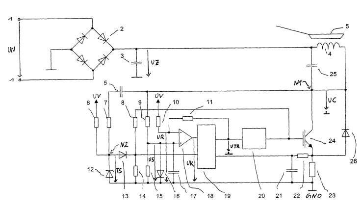
magnetically
coupled with the induction coil. The eddy currents bring about a heating of
the
cooking utensil.
[004] Numerous different circuit arrangements and drive methods are known for
driving the induction coil. It is common to all the circuit and method
variants that
they generate a high frequency drive voltage for the induction coil from a low
fre-
quency input supply voltage. Such circuits are known as frequency converters.
[005] For frequency converting or converting normally initially the input
supply or
alternating supply voltage is rectified with the aid of a rectifier into a
direct supply
voltage or intermediate circuit voltage and subsequently for generating the
high
frequency drive voltage processing takes place using one or more switching ele-
ments, generally insulated gate bipolar transistors (IGBTs). Normally a so-
called
CA 02625764 2008-04-10
2
intermediate circuit capacitor for buffering the intermediate circuit voltage
is pro-
vided at the rectifier output, i.e. between the intermediate circuit voltage
and a ref-
erence potential.
[006] A converter variant widely used in Europe is a half-bridge circuit
formed
from two IGBTs, a series resonant circuit being formed by the induction coil
and
two capacitors, which are looped in serial manner between the intermediate
circuit
voltage and the reference potential. The induction coil is connected by one
termi-
nal to a connection point of the two capacitors and by another terminal to a
con-
nection point of the two IGBTs forming the half-bridge. This converter variant
is
efficient and reliable, but relatively expensive due to the two IGBTs
required.
[007] An optimized variant from the costs standpoint consequently uses a
single
switching element or IGBT, the induction coil and a capacitor forming a
parallel
resonant circuit. Between the output terminals of the rectifier, parallel to
the in-
termediate circuit capacitor, are serially looped in the parallel resonant
circuit of
induction coil and capacitor and the IGBT. When operating this converter
variant
there is, however, a risk that under unfavourable operating conditions, e.g.
when
using an unfavourable cooking utensil, the components can become overloaded.
This normally leads to a reduced service life of such induction heating
devices.
PROBLEM AND SOLUTION
[008] The problem of the invention is therefore to provide a method for
operating
an induction heating device, a method for saucepan detection for an induction
heating device and an induction heating device, in which the induction heating
de-
vices have a frequency converter with a single switching element or IGBT and
which in the case of changing operating conditions permit a reliable,
component-
protecting operation in the case of a long service life of the induction
heating de-
vice.
[009] The invention solves this problem by a method for operating an induction
heating device according to claim 1, a method for saucepan detection for an in-
CA 02625764 2008-04-10
3
duction heating device according to claim 9 and an induction heating device ac-
cording to claim 10.
[010] Advantageous and preferred developments of the invention form the
subject
matter of the further claims and are explained in greater detail hereinafter.
By ex-
press reference the wording of the claims is made into part of the content of
the
description.
[0111 The inventive method is used for operating an induction heating device
with
an induction coil, a capacitor connected in parallel to the induction coil and
where
said induction coil and said capacitor form a parallel resonant circuit, and a
con-
trollable switching element, which is looped in in series with the parallel
resonant
circuit between an intermediate circuit voltage generated from an alternating
sup-
ply voltage and a reference potential and which is controlled in such a way
that
during a heating operation an oscillation of the parallel resonant circuit is
brought
about. For operating the induction heating device a low point of an
oscillating cy-
cle is determined at a connection node of the parallel resonant circuit and
the
switching element, a low point voltage is determined at the low point of the
oscil-
lating cycle and the switching element is switched on in the low point of the
oscil-
lating cycle for an on period, which is established as a function of the low
point
voltage in such a way that a low point voltage does not exceed a
predeterminable
maximum value in the following oscillating cycles. The maximum value is pref-
erably lower than 50 V, particularly preferably lower than 10 V. This permits
a
particularly component-protecting and therefore low-wear operation of the
induc-
tion heating device, because the switching element is switched on precisely
when
no or only a limited voltage is present at the connecting node of the parallel
reso-
nant circuit and the switching element. Thus, a switching through of the
switching
element only generates a negligible or no current peak in the actual switching
element and in the components of the induction heating device. Through the ap-
propriate choice of the on period the resonant circuit in the charging phase
is only
supplied with sufficient energy for the voltage at the connection node of the
paral-
lel resonant circuit and the switching element in the following oscillating
cycle to
oscillate through again to the desired voltage value, i.e. in the low or
reversal point
has the desired voltage level. If the on period is chosen too short, the
voltage at
CA 02625764 2008-04-10
4
the connection node in the following oscillation cycle in the low point has an
ex-
cessive value, so that on switching through the switching element a current
peak
occurs. If the on period is chosen too long, a maximum current loading of the
components, e.g. the switching element, can be exceeded, so that damage may
occur to the same. The reference voltage is preferably the earth or ground
poten-
tial. The switching element can be constituted by all suitable voltage-proof
switch-
ing elements and in particular high voltage-proof insulated gate bipolar
transistors
(IGBTs). The switching on time of the switching element is consequently syn-
chronized with the oscillation low points, the voltage level at the switching
on point
being used for determining the on period.
[012] In a further development of the method the on period is so determined or
set, that a low point voltage in the following oscillation cycles is equal to
the refer-
ence voltage. In this case there is a virtually currentless switching on
process of
the switching element.
[013] In a further development of the method the on period is increased com-
pared with the on period of a preceding oscillation cycle if the low point
voltage
exceeds a predetermined threshold value. This makes it possible to obtain a
stepwise adaptation or regulation of the low point voltage. If the low point
voltage
in an oscillation cycle n is too high, this means that in an oscillation cycle
n-1 too
little energy has been fed into the resonant circuit, i.e. the on period was
too short.
Thus, the on period must be increased, e.g. with a predetermined step width.
If in
the oscillation cycle n+1 the low point voltage again exceeds the threshold
value,
the on period is again increased. This process is repeated until the low point
volt-
age has reached the desired value, ideally 0 V. Starting from a low point
voltage
of 0 V, the on period can obviously be reduced during following oscillation
cycles
until the low point voltage is e.g. somewhat higher than 0 V, but lower than
an ad-
justable threshold value. This allows a dynamic tracking or follow-up of the
on pe-
riod if the resonant circuit parameters, e.g. due to a shifting of a cooking
vessel on
a hotplate, are subject to change.
[014] In a further development of the method the low point of the oscillation
or the
given oscillation cycles is determined by deriving or differentiating a
voltage gradi-
CA 02625764 2008-04-10
ent at the connection node of the parallel resonant circuit and the switching
ele-
ment. Through differentiation it is possible to easily determine the low point
of the
voltage gradient or an oscillation cycle, because there the differentiation
value is
zero.
[015] In a further development of the method no low point determination takes
place when the switching element is switched on. This makes it possible to pre-
vent the suppression of low points in the voltage gradient caused by a
switching
on of the switching element, because they are normally not necessary for
evalua-
tion or even interfere with the latter.
[016] In a further development of the method the low point voltage is compared
with a reference voltage and as a function of the result of the comparison a
com-
parison signal is produced indicating whether the low point voltage is higher
or
lower than the reference voltage. Preferably the reference voltage is
generated
as a function of the switching state of the switching element.
[017] In a further development of the method determination takes place as to
whether there is a cooking vessel on the cooking surface or heating zone
associ-
ated with the induction heating device, a cooking vessel being detected if in
the
range of a zero passage of the alternating supply voltage it is not possible
to de-
termine low points of oscillation cycles at the connection node of the
parallel reso-
nant circuit and the switching element. The damping of the resonant circuit is
highly dependent on whether or not there is a cooking vessel in a heating zone
of
the induction heating device. If a magnetically acting cooking vessel is
placed on
a cooking surface, resonant circuit damping strongly increases, because energy
is
removed from the resonant circuit and absorbed by the cooking vessel. In this
case the intermediate circuit voltage in the vicinity of a zero passage of the
alter-
nating supply voltage decreases so strongly that there is no longer the
formation
of an oscillation with detectable low points. If in the vicinity of the supply
zero
passage it is no longer possible to detect low points, it can be concluded
there-
from that a cooking vessel is present. This is possible continuously, also
during
active heating operation.
CA 02625764 2008-04-10
6
[018] In the inventive method for saucepan detection for an induction heating
de-
vice, which largely corresponds to the above-described induction heating
device,
the switching element is briefly closed, which excites an oscillation of the
parallel
resonant circuit. The number of oscillation cycles which occur is established
by
determining and counting the low points of the oscillation at a connection
node of
the parallel resonant circuit and the switching element. The presence of a
cooking
vessel or pot is determined as a function of whether the number of oscillation
cy-
cles drops below a predeterminable threshold value. As stated hereinbefore,
resonant circuit damping is dependent on whether or not there is a cooking
vessel
in a heating zone of the induction heating device. If a magnetically acting
cooking
vessel is placed on a hotplate or in a heating zone, the resonant circuit
damping
increases sharply. In this case, even after a few oscillation cycles or
periods it is
no longer possible to detect an oscillation and therefore also oscillation low
points.
If no cooking vessel is placed on a hotplate, the oscillation and therefore
the oscil-
lation low points can be detected for a much longer time, i.e. the number of
counted or countable low points is much larger than for more strongly damped
os-
cillation with a cooking vessel. The number of counted low points can
therefore
be used to indicate the presence of a cooking vessel.
[019] The inventive induction heating device, which is particularly suitable
for per-
forming one of the aforementioned methods, comprises an induction coil, a ca-
pacitor connected in parallel to the induction coil, said induction coil and
said ca-
pacitor forming a parallel resonant circuit, and a controllable switching
element
looped in in series with the parallel resonant circuit between an intermediate
cir-
cuit voltage and a reference voltage and which is controlled in such a way
that
during a heating operation the parallel resonant circuit is made to oscillate.
Ac-
cording to the invention there is a low point determination device for
determining a
low point of an oscillation cycle at a connection node of the parallel
resonant cir-
cuit and the switching element, a low point voltage determination device for
de-
termining a low point voltage at the low point of the oscillation cycle and a
control
device coupled to the low point determination device and the low point voltage
de-
termination device and which is set up in such a way that the switching
element is
switched on for an on period in the oscillation cycle low point and which is
estab-
lished as a function of the low point voltage in such a way that a low point
voltage
CA 02625764 2008-04-10
7
in the following oscillation cycles does not exceed a predeterminable maximum
value. The control unit can e.g. be a microcontroller.
[020] In a further development of the induction heating device the low point
de-
termination device comprises a first capacitor, a first resistor, an
overvoltage sup-
pressor, particularly a Zener diode, and a second resistor, the first
capacitor, the
first resistor and the overvoltage suppressor being looped in serially between
the
connection node of the parallel resonant circuit and the switching element and
a
reference potential and the second resistor is looped in between a supply
voltage
and a connection node of the first resistor and the overvoltage suppressor and
a
low point signal is present at the connection node of the first resistor and
the over-
voltage suppressor and said signal indicates a low point. Said components form
a
differentiator, which differentiates or derives a voltage gradient at the
connection
node of the parallel resonant circuit and the switching element. This makes it
eas-
ily possible to implement a low point detection of the voltage gradient,
because at
the transition from a negative to a positive slope of the voltage gradient a
rising
slope of the low point signal is produced. As a result of the second resistor
in the
case of a constant voltage at the connection node the low point signal is
raised to
a supply voltage level.
[021] In a further development of the induction heating device the low point
volt-
age determination device comprises a voltage divider looped in between the con-
nection node of the parallel resonant circuit and the switching element and a
ref-
erence potential and which produces a divided down resonant circuit voltage, a
reference voltage generating device for generating a reference voltage and a
comparator, which is supplied with the resonant circuit voltage and the
reference
voltage and as a function thereof generates a comparator signal indicating
whether the resonant circuit voltage is higher or lower than the reference
voltage.
Preferably the low point determination device comprises a delay element, which
outputs the resonant circuit voltage with a time delay to the comparator. This
permits a facilitated evaluation of the comparator signal in the control unit.
CA 02625764 2008-04-10
8
[022] In a further development of the induction heating device the reference
volt-
age generating device is set up in such a way that the reference voltage is
gener-
ated as a function of the switching state of the switching element.
[023] These and further features can be gathered from the claims, description
and drawings and the individual features, both singly or in the form of
subcombi-
nations, can be implemented in an embodiment of the invention and in other
fields
and can represent advantageous, independently protectable constructions for
which protection is claimed here. The subdivision of the application into
individual
sections and the subheadings in no way restrict the general validity of the
state-
ments made thereunder.
BRIEF DESCRIPTION OF THE DRAWINGS
[024] Embodiments of the invention are described hereinafter relative to the
at-
tached diagrammatic drawings, wherein show:
Fig. 1 A circuit diagram of an embodiment of an induction heating device.
Fig. 2 Signal curves of signals of the induction heating device of fig. 1
during a
heating operation.
Fig. 3 Signal curves of the signals of fig. 2 during a saucepan detection,
when no
saucepan is present.
Fig. 4 Signal curves of the signals of fig. 2 during a saucepan detection when
a
saucepan is present.
DETAILED DESCRIPTION OF THE EMBODIMENTS
[025] Fig. 1 shows a circuit diagram of an embodiment of an induction heating
device with connecting terminals 1 for the connection of an alternating supply
voltage UN, e.g. of 230 V, 50 Hz supply frequency and which is rectified by a
bridge rectifier 2. A so-called intermediate circuit voltage UZ is applied to
an out-
CA 02625764 2008-04-10
9
put of the bridge rectifier 2 and this is buffered by an intermediate circuit
capacitor
3.
[026] An induction coil 4 and a capacitor 25 are connected in parallel and
form a
parallel resonant circuit. A controllable switching element in the form of an
IGBT
24 and a current sensing resistor 23 are looped in serially with the parallel
reso-
nant circuit between the intermediate circuit voltage UZ and a reference
potential
in the form of the earth or ground voltage GND. The IGBT 24 is controlled by a
control unit in the form of a microcontroller 19 and for generating the
necessary
drive level of the IGBT 24 a drive circuit 20 is looped in between a control
output
of microcontroller 19 and the gate terminal of the IGBT 24. A freewheeling
diode
26 is connected in parallel to the collector-emitter junction of the IGBT 24.
A
measuring voltage at the current sensing resistor 23 is filtered by a RC
filter from
resistor 22 and capacitor 21 and applied to an associated input of
microcontroller
19.
[027] Following the application of the alternating supply voltage UN or if the
in-
duction heating device is not subject to a heating operation, the intermediate
cir-
cuit capacitor 3 is charged to a peak value of the alternating supply voltage
UN,
e.g. 325 V in the case of a 230 V alternating supply voltage. If the IGBT 24
is
switched on starting from this state, a voltage UC at the collector of the
IGBT or at
a connection node N1 of the parallel resonant circuit and the IGBT assumes
roughly a ground potential GND, because the current sensing resistor 23 is di-
mensioned in very low resistance manner.
[028] Therefore the capacitor 25 is charged to the value of the intermediate
circuit
voltage UZ. As the induction coil 4 is also supplied with the intermediate
circuit
voltage UZ, there is a linear current rise through the induction coil 4, so
that mag-
netic energy is stored in the coil.
[029] If the IGBT 24 is switched off, an oscillation is formed in the resonant
circuit
whose amplitude at the collector of IGBT 24 can rise well above the value of
the
intermediate circuit voltage UZ. This oscillation e.g. induces in a bottom of
a
cooking vessel 5 standing over induction coil 4 an eddy current which brings
about
CA 02625764 2008-04-10
the heating thereof. As a result energy is extracted from the resonant circuit
and
the oscillation is damped.
[030] Ideally the induction heating device is so operated and the IGBT 24 so
con-
trolled that the resonant circuit during the charging phase, i.e. with the
IGBT 24
switched through, is supplied with just enough energy for the voltage UC at
node
N1 or at the collector of IGBT 24 oscillate through in a following oscillation
cycle to
the ground potential GND. For this purpose there must be an appropriate choice
of the on period of IGBT 24. Precisely at the time where voltage UC at node N1
has reached its lowest potential, i.e. in the low point of an oscillation
cycle, IGBT
24 must be switched on again in order to recharge the resonant circuit for the
fol-
lowing oscillation cycle or following period. If in the low point the voltage
UC at
node N1 oscillates through to ground potential, on switching on IGBT 24 there
are
no switch-on current peaks through IGBT 24 or capacitor 25, which ensures a
component-protecting operation.
[031] However, if in a preceding oscillating cycle insufficient energy has
been
= transferred into the resonant circuit, i.e. the on period has been chosen
too short,
the voltage UC at node N1 does not oscillate through to ground potential GND,
so
that prior to the switching on of IGBT 24 in the oscillation low point there
is a volt-
age difference between collector and emitter of IGBT 24 or ground. When IGBT
24 is switched on this leads to a current peak through IGBT 24 and capacitor
25,
because for the voltage jump at its terminal capacitor 25 virtually represents
a
short-circuit and is very rapidly charged. This is prejudicial both to IGBT 24
and
capacitor 25 and leads to a reduced service life of said components.
[032] In order to permit a switching on of IGBT 24 in the low point of an
oscillation
cycle at node N1, a low point determination device is provided in the form of
a ca-
pacitor 5, a resistor 7, an overvoltage suppressor in the form of a Zener
diode 12
and a resistor 6, the capacitor 5, resistor 7 and Zener diode 12 being looped
in
serially between the connection node N1 and ground potential GND and resistor
6
is looped in between a supply voltage UV and a connection node N2 of resistor
7
and Zener diode 12. A signal or a voltage TS is present at connection node N2
and its curve indicates a low point.
CA 02625764 2008-04-10
11
[033] The voltage UC at node N1 or between the collector and emitter of IGBT
24
is derived or differentiated by capacitor 5, resistor 7 and resistor 6, i.e.
during or
shortly after the low point of an oscillation cycle at node N1 a rising slope
of volt-
age TS arises. The Zener diode 12 limits the occurring voltage level of
voltage TS
to values which can be processed by microcontroller 19, e.g. to approximately
0.6
to 5.6 V. With a rising oscillation at node N1 the voltage TS e.g. assumes
values
of approximately +5 V and with a falling oscillation e.g. values of
approximately -
0.6 V.
[034] If there is no change to the voltage UC at node N1, e.g. if IGBT 24 is
switched on, a positive potential is applied across resistor 6 to the cathode
of
Zener diode 12. Therefore there is a positive voltage slope at Zener diode 12
or
voltage TS, if the differentiated voltage at node N1 changes from negative
values
to positive values or from negative values to a value of zero. The voltage TS
is
transmitted for evaluation across a diode 13 to an associated input of
microcon-
troller 19.
[035] Thus, by means of a rising slope of voltage TS, microcontroller 19 can
de-
tect a low point of an oscillation cycle at node N1 and switching in the IGBT
24
synchronously to the low point.
[036] However, if at the switching on point the voltage UC at node N1 is
higher
than 0 V, as a result of the switching on of IGBT 24 there is initially a
negative
slope of voltage UC at node N1, so that the signal TS again passes to a low
level
from a positive level resulting from the previously detected low point. Since
in the
case of switched through IGBT 24 the voltage UC at node N1 remains roughly
constant at ground potential, due to the resistor 6 there is again a positive
slope of
voltage TS. This would indicate a further oscillation low point to
microcontroller
19. However, as the low point has not been caused by the oscillation, but by
the
switching on of the IGBT at voltages higher than 0 V, said second positive
slope of
voltage TS is not transmitted to microcontroller 19.
CA 02625764 2008-04-10
12
[037] For this purpose a control or drive voltage of IGBT 24 is divided down
and
coupled back to an evaluatable level by a voltage divider formed from
resistors 8
and 14. The diode 13, which is looped in between voltage TS and the associated
input of microcontroller 19, in conjunction with the coupled back control or
drive
voltage leads to the second rising slope of voltage TS being transmitted to
the in-
put of microcontroller 19. Thus, there is no low point determination with the
IGBT
24 switched on.
[038] To determine the voltage UC at node N1 in the low point of an
oscillation
cycle, the determined voltage at the low point forming the basis for the
calculation
of the on period of IGBT 24, a low point voltage determination device in the
form
of a voltage divider formed by resistors 9 and 15 looped in between the connec-
tion node N1 and ground GND and generating a divided down resonant circuit
voltage US, a reference voltage generating device with resistors 10 and 11 for
generating a reference voltage UR and a comparator 18 are provided, which is
supplied with the resonant circuit voltage US and reference voltage UR and as
a
function thereof generates a comparator signal UK indicating whether the reso-
nant circuit voltage US is higher or lower than reference voltage UR and is
applied
to an associated input of microcontroller 19 for evaluation purposes.
[039] The resonant circuit voltage US is limited by a diode 16 to
approximately
0.7 V and is looped in between the input of comparator 18 to which the
resonant
circuit voltage US is applied and ground GND. A capacitor 17 connected in
paral-
lel to diode 16 ensures that the change to the voltage UC at node N1 is only
effec-
tive with a slight delay at the input of comparator 18.
[040] The resistors 10 and 11 for generating reference voltage UR are serially
looped in between the control output of microcontroller 19 for controlling or
driving
IGBT 24 and the supply voltage UV, the reference voltage UR being at the con-
nection node between resistors 10 and 11. Reference voltage UR is consequently
generated as a function of the switching state of the switching element or the
level
of a voltage UTR at the control output of microcontroller MC. Resistors 10 and
11
are dimensioned in such a way that, with the IGBT 24 switched on, the
reference
CA 02625764 2008-04-10
13
voltage UR is lower than the forward voltage of diode 16 and with the IGBT 24
switched off is higher than the forward voltage of diode 16.
[041] Thus, with the IGBT 24 switched off, independently of the voltage UC at
node N1, the comparator signal UK always indicates that the resonant circuit
volt-
age US is lower than the reference voltage UR.
[042] With IGBT 24 switched on, at the end of the time lag of the voltage at
node
N1 or the resonant circuit voltage US produced by capacitor 17, the resonant
cir-
cuit voltage US is approximately 0 V, because with the IGBT 24 switched on or
through approximately 0 V is present at the collector or at node N1. Thus, at
the
end of the time lag, the comparator signal UK always indicates that the
resonant
circuit voltage US is lower than the reference voltage UR.
[043] Since, as a result of capacitor 17, the resonant circuit voltage US is
always
applied with a delay to comparator 18, a value of the resonant circuit voltage
US
belonging to a switching on time of IGBT 24 is compared with a reference
voltage
value belonging to a switched on IGBT 24. Thus, as a result of the delay of
the
resonant circuit voltage US on switching on IGBT 24 there is a pulse of
compara-
tor signal UK if the resonant circuit voltage US at the time of switching on
is higher
than the reference voltage UR with IGBT 24 switched on. This pulse indicates
to
microcontroller 19 that the voltage UC at node N1 in the oscillation cycle low
point
is higher than a maximum value corresponding to the reference voltage value.
[044] This means that the energy fed into the resonant circuit during the
preced-
ing on period was not sufficient to allow the voltage UC at node N1 to
oscillate
through to ground potential GND. Thus, compared with the preceding oscillation
cycle the on period is increased. If the voltage UC at node N1 in the low
point of a
following oscillation cycle is lower than the maximum value corresponding to
the
reference voltage value, the on period remains constant. The described method
steps are repeated periodically.
[045] In summarizing, the induction heating device is operated in such a way
that
the switching on time of the IGBT 24 is synchronized with the low point of
voltage
CA 02625764 2008-04-10
14
UC at node N1 or the collector voltage. The on period or switching off time of
the
IGBT 24 is determined by the minimum resonant circuit energy necessary for os-
cillating through voltage UC at node N1 to ground potential with IGBT 24
switched
off. For determining the associated on period the microcontroller 19 increases
the
on period of IGBT 24 until the voltage UC at the switching on time, i.e. in
the oscil-
lation low point, is lower than a predefined value close to 0 V. This on
period or
this operating point corresponds to the lowest continuous power output. Lower
power levels are set by the use of the conventional, so-called 1/3 or 2/3 half-
wave
operation and optionally additional cycles of the IGBT 24 by periodic
switching on
and off. A power increase within a half-wave is possible through increasing
the on
period to beyond the aforementioned minimum on period.
[046] For illustrating the operation of the induction heating device, fig. 2
shows
the voltage UC, the signal or voltage TS and the voltage UTR at the control
output
of microcontroller 19 used for controlling driver 20 or IGBT 24. A low level
of volt-
age UTR brings about a switching through of IGBT 24 and a high level leads to
a
blocking action. With IGBT 24 switched on, the voltage UC is approximately 0 V
and the voltage TS approximately 5 V.
[047] As soon as IGBT 24 is switched off, voltage UC increases roughly sinusoi-
dally in a first oscillation cycle. Voltage TS remains unchanged at
approximately 5
V. When voltage UC has exceeded its peak value, it decreases sinusoidally to
approximately 0 V. Voltage TS drops slowly to approximately 0 V.
[048] At the low point of the first oscillation cycle there is a positive
slope of volt-
age TS indicating the low point to microcontroller 19. Consequently this
changes
the voltage UTR at its control output and in the case shown a level of 0 V of
volt-
age UTR brings about a switched on IGBT 24. The IGBT remains switched on or
the voltage UTR remains at a level of 0 V until the energy fed into the
resonant
circuit is just sufficient for the voltage UC to oscillate through again to 0
V in a fol-
lowing, second oscillation cycle. The method described is repeated for the
follow-
ing oscillation cycles.
CA 02625764 2008-04-10
[049] For saucepan or pot detection, i.e. for establishing whether the cooking
vessel 5 is located in a heating zone associated with induction coil 4, in the
vicinity
of the zero passages of the input supply voltage UN monitoring takes place to
es-
tablish whether low points can be determined, i.e. whether rising slopes of
the
voltage TS occur within a time interval in which experience has shown that
rising
slopes must occur. If a cooking vessel 5 is present the resonant circuit is
highly
damped, i.e. the intermediate circuit capacitor 3 is approximately completely
dis-
charged in the zero passage area. In this case the intermediate circuit
voltage UZ
is no longer adequate for generating rising slopes of voltage TS in the supply
zero
passage area. This can be used for saucepan detection during active heating op-
eration.
[050] For saucepan detection with non-active heating operation, e.g. if an
opera-
tor sets a desired heating power of a hotplate and for enabling a heating
power
generation it is necessary to establish whether there is a cooking vessel 5 on
the
hotplate, use can be made of the method illustrated in figs. 3 and 4.
[051] Fig. 3 shows signal curves of signals of fig. 2 during saucepan
detection,
when no saucepan is present, whilst fig. 4 shows signal curves during saucepan
detection when a saucepan is present.
[052] At the start of saucepan detection, initially through a brief voltage
pulse of
voltage UTR IGBT 24 is briefly switched through which excites an oscillation
of the
parallel resonant circuit. A positive slope of voltage TS is generated in each
low
point of the oscillation cycle of voltage UC. Microcontroller 19 counts the
positive
slopes and therefore the number of oscillation cycles which occur.
[053] Since due to the absence of a cooking vessel the resonant circuit
damping
is limited in fig. 3, a large number of slopes are counted. Due to the strong
damp-
ing of the resonant circuit in fig. 4 only approximately five rising slopes
are detect-
able there.
[054] If a threshold value of e.g. ten slopes is fixed for saucepan detection,
in fig.
3 the slopes or number of low points exceed the fixed threshold value, i.e. by
defi-
CA 02625764 2008-04-10
16
nition there is no cooking vessel in the heating zone. As the number of slopes
in
fig. 4 is below the threshold value, it can be concluded that there is a
cooking ves-
sel in the heating zone.
[055] The evaluation of the low points or the use of the low point
determination
device can consequently be used for the optimum operation of the induction
heat-
ing device and for saucepan detection during a heating operation and also for
saucepan detection for enabling the heating operation.
[056] The embodiments shown permit a reliable, component-protecting operation
of the induction heating device although the latter has a frequency converter
with
a single switching element or single IGBT.