Note: Descriptions are shown in the official language in which they were submitted.
CA 02626532 2012-06-15
BIOCHIP WITH CHANNEL-DEFINING PROTECTION FILM
FIELD
The following description relates generally to a bio chip and an apparatus for
analyzing
biological material capable of analyzing a variety of specific materials
included in
biological materials using a single bio chip, and capable of automatically
conducting
blood-collecting, sterilization and analysis.
BACKGROUND
A bio sensor may include a series of devices for immobilizing molecules having
a
biological activity on the surface of a solid small thin film by utilizing
covalent bonding
or non-covalent bonding and for changing interactions or bonding in biological
materials to an electrical signal useful for monitoring and assaying gene
expression,
gene mutation, gene polymorphism and the like.
Bio sensors may also be called bio chips in a broader sense that includes
micro devices
for assaying biological molecules quantitatively and qualitatively. Bio chips
may be
categorized into three types based on thin film material formed on a solid
substrate and
targets to be assayed, that is, a DNA chip, a cell chip and a protein chip.
SUMMARY
Structures for assaying a single specific material included in biological
materials are
described, which may compare to conventional bio chips by increasing and/or
otherwise
improving production efficiency, yield, and applicability and while reducing
wasting of
raw materials.
In accordance with one aspect of the present invention, there is provided a
bio chip for
analyzing biological material. The bio chip includes a substrate and a
protection film
positioned on the substrate. The protection film having an inlet port
structured to
receive injected biological materials, a plurality of first through-holes that
expose the
substrate, and micro channels each connected to the inlet port and to a
respective first
through hole. The bio chip further includes reaction-inducing materials
immobilized on
portions of the substrate positioned at and exposed by the first through
holes.
1
CA 02626532 2011-05-09
The bio chip may include at least one electrode pad positioned on the
substrate, and
electrode lines connected to the electrode pad, and the protection film may be
structured
to define at least one second through hole that exposes a first portion of the
electrode
pad and micro channels connecting the at least one second through hole with
the inlet
port.
The at least one second through hole defined by the protection film may expose
distal
ends of the electrode lines connected to a second portion of the electrode
pad.
The width of each micro channel may be in the range of 0.1mm tolmm.
The micro channels may be positioned inside the protection film or on an upper
surface
of the protection film.
The inlet port may be formed at a side surface of the protection film.
The protection film may include an isolation film positioned on the substrate,
and a
polymer film formed on the isolation film and the micro channels may be
positioned at
one side of the polymer film.
The bio chip may include an upper substrate positioned on the protection film.
The bio chip may include a sterilizer positioned at an upper surface of the
upper
substrate.
The sterilizer may include a groove positioned at the upper surface of the
upper
substrate, and sterilization material inside the groove.
The sterilizer may further include a cover layer at least partially covering
the groove
and adhered to the upper substrate.
The sterilizer may include sterilization material positioned at the upper
surface of the
upper substrate, and a cover layer at least partially covering the
sterilization material
and adhered to the upper substrate.
2
CA 02626532 2011-05-09
The bio chip may include a mesh structure positioned within the groove and
capable of
absorbing the sterilization material.
The sterilization material may include at least one or more components
selected from a
group consisting of sterilizer, antibiotic, biocide, anesthetic, peroxidic
sterilizer,
halogen sterilizer and alcoholic sterilizer.
The bio chip may include a treatment unit positioned at the upper surface of
the upper
substrate.
The treatment unit may include a groove positioned on an upper surface of the
upper
substrate, and a treatment material inside the groove.
The treatment material may include at least one or more components selected
from a
group consisting of glycerin, propylene glycol, butylen glycol, polyethylene
glycol,
sorbitol, trehalose, sodium PCA, hyaluron acid, collagen and betaine.
In accordance with another aspect of the invention there is provided a bio
chip for
analyzing biological material. The bio chip includes a substrate, at least one
electrode
pad positioned at an upper surface of the substrate, and electrode lines
connected to the
electrode pad. The bio chip also includes a protection film, positioned at an
upper
surface of the substrate, and structured to define through holes that expose
the electrode
pad, and to define micro channels each connecting the through holes to an
inlet port into
which biological materials are injected. The electrode lines have distal ends
exposed at
an associated through hole. The bio chip further includes reaction-inducing
materials
immobilized on the distal ends of the electrode lines exposed at each through
hole.
Implementations of these aspects may include one or more of the following
effects.
One single biological material can be injected into a single bio chip to
analyze a variety
of specific materials included in the biological materials.
3
CA 02626532 2011-05-09
Optical measurement and electro-chemical measurement can be simultaneously
conducted to improve the efficiency.
The biological material can be supplied from an inlet port to a reaction
region by way of
a capillary phenomenon in micro channels, dispensing with any special
manipulation
from outside.
The bio chip can be formed with a sterilizer to allow any vulnus caused by,
i.e., blood
collection to be swiftly sterilized to the enhanced convenience to a user.
Collected blood can be supplied to the reaction region upon blood collection
to allow a
swift analysis of the blood.
The bio chip is formed with a sterilizer for sterilizing any vulnus caused by
blood
collection and a treatment unit for treating the vulnus.
The apparatus for analyzing the biological material is formed with a laser
beam source
to enable a swift blood collection, and is also formed with a device for
transferring the
bio chip provided with the sterilizer to allow the bio chip to be transferred
for automatic
blood collection, sterilization and analysis.
BRIEF DESCRIPTION OF THE DRAWINGS
FIG. 1 is a schematic plan illustrating a bio chip according to a first
exemplary
implementation.
FIG. 2 is a schematic plan illustrating another bio chip according to a first
exemplary
implementation.
FIGS. 3A and 3B are a schematic plan and a cross-sectional view illustrating
still
another bio chip according to a first exemplary implementation.
FIG. 4 is a cross-sectional view illustrating a bio chip formed on a top
surface of a
substrate according to the first exemplary implementation.
FIGS. 5A and 5B are a schematic plan illustrating micro channels formed on a
protection film of the bio chip according to the first exemplary
implementation.
FIG. 6 is a schematic plan illustrating a bio chip formed on a top surface of
a substrate
according to the first exemplary implementation.
3a
CA 02626532 2008-03-19
collecting blood from a bio chip of the second implementation immobilized on
an
apparatus for analyzing another biological material.
FIG.19 is a schematic concept representation illustrating an operation of
transferring a
bio chip from an apparatus for analyzing biological material.
DETAILED DESCRIPTION
Hereinafter, a bio chip and an apparatus for analyzing biological material in
accordance
with the exemplary implementations will be described in detail referring to
the
accompanying drawings.
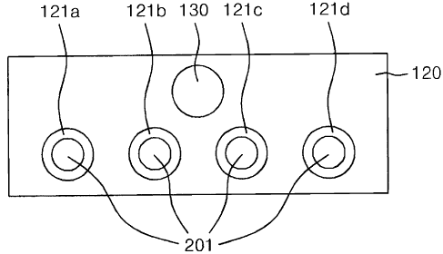
Referring to FIG.1, a bio chip for analyzing biological material includes: a
substrate; a
protection film (120) formed on the substrate with first through holes (121a,
121b, 121c,
121d) for exposing the substrate, micro channels each connected to the first
through
holes (121a, 121b, 121c, 121d), and an inlet port (130) into which biological
materials
are injected by being connected to the micro channels; and reaction-inducing
materials
(201) each immobilized on the substrate at a position that is exposed
to/through the first
through holes.
It should be noted for reference that FIG.1 does not illustrate the substrate
and the micro
channels.
In the bio chip, thus constructed, biological materials may be injected into
the inlet port
(130), and the biological materials may be supplied to the first through holes
(121a,
121b, 121c, 121d) from the inlet port (130) via the micro channels. The
biological
materials supplied to the first through holes (121a, 121b, 121c, 121d) may be
reacted
with the reaction-inducing materials (201), where the reacted degree is
optically
measured, and the measured reacted degree is utilized to analyze the
biological
materials.
The reaction-inducing materials (201) may include different reaction-inducing
materials. In other words, the reaction-inducing materials respectively
located at a
position on the substrate corresponding to and exposed to/through the first
through
holes (121a, 121b, 121c, 121d) may be respectively different reaction-inducing
materials, which correspondingly react with various specific materials
included in the
supplied biological materials, whereby reactions may be optically measured
from each
of the first through holes (121a, 121b, 121c, 121d).
For example, if one reaction-inducing material reacts with cholesterol, and
another
reaction-inducing material reacts with hemoglobin, said one reaction-inducing
material
may react with the cholesterol contained in the biological material while said
another
reaction-inducing material may react with hemoglobin. Therefore, one
biological
material can be injected into one bio chip to effect analysis of various
specific materials
contained in the biological material. The biological materials may be, for
instance, body
fluid including blood, urine, serum and saliva.
Referring to FIG.2, a bio chip for analyzing biological material comprises: a
substrate
4
CA 02626532 2008-03-19
(100) formed with electrode pads (150) and electrode lines (151) each
connected to the
electrode pads (150); a protection film (120) formed on the substrate (100)
exposing the
electrode pads (150) and mounted with second through holes (122a, 122b, 122c,
122d)
exposing distal ends of the electrode lines (151), micro channels each
connected the
second through holes (122a, 122b, 122c, 122d), and an inlet port (130)
connected to the
micro channels and into which biological materials are injected; and reaction-
inducing
materials (201) immobilized on the distal ends of the electrode lines (151)
exposed to
each second through hole (122a, 122b, 122c, 122d). In other words, the bio
chip works
in such a fashion that the biological materials respectively supplied to the
second
through holes (122a, 122b, 122c, 122d) react with the reaction-inducing
materials (201),
and a reaction degree is electro-chemicall y measured.
The distal ends of the electrode lines (151) may be connected to the electrode
pads
(150), while the other ends of the electrode lines (151) may be dispersed to
be
positioned within the second through holes (122a, 122b, 122c, 122d).
A screen print may be employed to form pasted electrode material, which is
plasticized
at a predetermined temperature to form the electrode pads (150) and the
electrode lines
(151), or photolithography process may be used to form the electrode pads
(150) and the
electrode lines (151). The distal ends of the electrode lines (151) that are
used for
measurement may comprise varying sizes and shapes, and two or more electrodes
may
be used for each measurement case.
FIGS.3A and 3B are a schematic plan and a cross-sectional view illustrating
still
another bio chip according to a first exemplary implementation, where the bio
chip may
be mixedly formed with the first through holes for optical measurement of
FIG.1, and
formed with second through holes for electro-chemical measurement of FIG 2.
In other words, a top of the substrate (100) of the bio chip as in FIG A may
be further
formed with the electrode pads and electrode lines respectively connected to
the
electrode pads, the protection film may expose the electrode pads, and the
protection
film may be further formed with at least one or more second through holes
exposing the
distal ends of the electrode lines and micro channels connecting the second
through
holes and the inlet port.
As illustrated in FIG3A, the protection film (120) of the bio chip may be
formed on the
substrate (100) exposing the electrode pads (150), and is formed with the
first through
holes (121a, 121b, 121c) and second through hole (122).
As illustrated in FIG3B, the first through holes (121a, 121b, 121c) may
contain only the
reaction-inducing material (201), and the second through hole (122) contains
the
electrode lines (151) and the reaction-inducing material (201). Thus, the
optical
measurement and electro-chemical measurement can be simultaneously conducted
to
enhance the efficiency.
Referring to FIG.4, the protection film (120) of the bio chip may be formed
thereon with
an upper substrate (170). The upper substrate (170) may be formed with a main
inlet
CA 02626532 2008-03-19
port communicating with the inlet port formed at the protection film (120) of
the bio
chip. The biological material may be injected into the main inlet port of the
upper
substrate (170), and the biological material injected into the main inlet port
may pass
through the inlet port formed at the protection film (120) and the micro
channels to be
supplied to the first and second through holes.
The substrate (100) foamed underneath the bio chip and the upper substrate
(170) may
be transparent. In other words, one of the substrate (100) and the upper
substrate (170)
or both the substrates (100, 170) be made of transparent substrates to allow
optically
measuring the reaction of the biological materials.
In FIGS. 5A and 513, the micro channels of bio chip is formed inside or on the
protection film. In other words, micro grooves may be formed on the protection
film
(120) to embody the micro channels (126a) as shown in FIG.5A, and as depicted
in
FIG.5B, micro paths may be formed inside the protection film (120) to embody
the
micro channels (126b). The width of each micro channel ranges from 0.1nmm-lmm,
typically.
The length of each micro channels may be the same so that the biological
materials can
be uniformly supplied from the inlet port (130) to the first through holes
(121a, 121b,
121c) and second through holes (122). The micro channels are manufactured
using
micro-fluidic control technique, such that biological materials can be
supplied from the
inlet port (130) to the first through holes (121a, 121b, 121c) and second
through holes
(122) according to capillary phenomenon without any special manipulation.
The micro-fluidic control technique separate blood corpuscles including red
corpuscle
and white corpuscle from blood elements including blood plasma but excluding
cells,
and the separated blood elements are supplied from the inlet port (130) to the
first
through holes (121a, 121b, 121c) and second through holes (122) via the micro
channels. Notably, different of the capillaries may be differently configured
to enable
routing of different aspects of a single introduced biological material to
different areas
of the substrate for reaction with the same or different reaction-inducing
materials
located at those sites, yielding concurrently observable test results.
Referring to FIG.6, the substrate (100) may be formed thereon with electrode
pads (150)
and electrode lines (151) each connected to the electrode pads (150).
Distal ends of the electrode lines (151.) may be positioned at a substrate
region formed
with the second through holes for clectro-chemically measuring the reaction
degree of
specific materials and the reaction-inducing materials included in the
biological
materials.
The distal ends of the electrode lines (151) may be configured in the form of
pads (A, B,
C) to easily detect the reaction degrees of the specific materials and the
reaction-
inducing materials contained in the biological materials.
The circular dotted lines (202) in FIG.6 indicate a region where the reaction-
inducing
6
CA 02626532 2008-03-19
materials are immobilized. As shown, a substrate region where the single
second
through hole is formed is arranged with three electrode lines, where the three
electrode
lines are respectively a working electrode, a reference electrode and a
counter electrode.
Referring to FIG.7, an inlet port (131) of the bio chip may be formed at a
lateral surface
of the protection film (120). In the case where an upper substrate is formed
on the
protection film (120), a main inlet port may be formed at a lateral surface
region of the
upper substrate correspondingly opposite to the inlet port (131) formed at the
protection
film (120) to thereby enlarge an inlet port area.
Now, referring to FIG.8, the protection film (120) may include an isolation
film (127)
formed on the substrate (100) and a polymer film (128) formed on the isolation
film
(127). The isolation film (127) and the polymer film (128) may be formed with
openings (127a, 127b, 127c, 128a, 128b, 128c) correspondingly opposite to the
substrate (100) region for measuring the reaction degrees of the specific
materials and
reaction-inducing materials contained in the biological materials.
The polymer film (128) may be laterally formed with an inlet port (131), and
the
polymer film (128) may be formed with micro channels (126a, 126b, 126c) for
connecting the inlet port (131) to the openings (128a, 128b, 128c) formed at
the
polymer film (128).
In a case where the protection film (120) is formed thereon with an upper
substrate
(170), a main inlet port (175) may be formed at a lateral surface of the upper
substrate
(170) correspondingly opposite to the inlet port (131) formed at the
protection film
(120).
As shown, the upper substrate (170) is formed with a transparent substrate
through
which light can pass. Alternatively, an opaque material film may be formed at
the upper
substrate (170), such that light can pass through only the region
correspondingly
opposite to the openings (127a, 127b, 127c, 128a, 128b, 128c) formed at the
isolation
film (127) and the polymer film (128).
As a result, the upper substrate (170) may be formed with light permissible
regions
(171, 172, 173) for passing irradiated light through for measuring the
reaction degrees
of the specific materials and reaction-inducing materials contained in the
biological
materials. The isolation film (127) may be formed at regions except for the
distal ends
of the electrode lines and the electrode pads for measurement.
The polymer film (128) may be embodied by forming at the isolation film (127)
with a
double-sided tape coated with adhesive polymer materials, or by printing on
the
isolation film (127) with polymer film materials.
FIG.9 is a schematic perspective view illustrating a bio chip according to a
second
exemplary implementation, where the bio chip according to the second
implementation
further includes a sterilizer (270) in addition to the chip structure of the
first
implementation.
7
CA 02626532 2008-03-19
To be more specific, the sterilizer (270) is formed on an upper substrate
(250) in the bio
chip structure formed with the upper substrate on the protection film, whereby
blood is
collected by a user who injects the collected blood into an inlet port (230)
of the bio
chip, and the finger vulnus caused by the blood collection can be sterilized
by the
sterilizer (270) provided at the bio chip.
With the sterilizer formed at a bio chip, blood may be injected the moment the
blood is
collected to assay the blood, and a finger vulnus caused by the blood
collection may be
swiftly sterilized by a sterilizer, allowing implementing a variety of
functions with a
single bio chip to the convenience of a user.
For reference, the inlet port (230) is formed in the shape of a through hole
that has
penetrated the upper substrate (250) and the protection film. Furthermore,
FIG.10 is a
schematic plan illustrating a state of the sterilizer (270) provided at a bio
chip, where the
inlet port (231) into which the biological materials are injected is formed at
a lateral
surface of the upper substrate (250) and the protection film.
Now, referring to FIGS. 11A and 11B, the sterilizer of the bio chip may
include a groove
(252) formed on the upper substrate (250), and a sterilization material (257)
filled inside
the groove (252) (see FIG h A).
The sterilizer may also include a cover layer (258) covering the groove (252)
and
adhered to the upper substrate (250).
If the cover layer (258) is further included at the sterilizer, leakage of
sterilization
material (257) from the sterilizer can be prevented, and if a user is to
conduct
sterilization, the sterilization can be performed at the sterilizer by
removing the cover
layer (258). As shown in FIG.11B, the sterilizer (270) includes the
sterilization material
(257) formed on the upper substrate (250), and the cover layer (258) adhered
to the
upper substrate (250) and for covering the sterilization material (257).
The sterilization material (257) may include at least one or more components
selected
from a group consisting of sterilizer, antibiotic, biocide, anesthetic,
peroxidic sterilizer,
halogen sterilizer and alcoholic sterilizer. The peroxidic sterilizer includes
hydrogen
peroxide, sodium preborate, potassium permanganate, benzoly peroxide and
peroxyacetic acid, and 2.53.5 % of hydrogen peroxide solution is largely used
for the
peroxidic sterilizer.
The halogen sterilizer may include chlorine or iodine which oxidizes cell
membranes of
microorganisms and protein of protoplasm to perform the sterilization and
disinfection
effect against various microorganisms. 2% of iodine solution or 9-12% of
povidone
iodine solution is largely used for the halogen sterilizer.
The alcoholic sterilizer may include ethanol and isopropanol, and 70% of
ethanol is
largely used for alcoholic sterilizer. The alcohol for disinfection has a
strong osmotic
power to easily penetrate membranes of surfaces of bacteria. The ethanol can
penetrate
the bacteria membranes to coagulate the protein of bacteria or transform the
cell
8
CA 02626532 2008-03-19
membranes of bacteria to kill the bacteria for disinfection.
Referring to FIG.12, the sterilizer formed on the upper substrate of the bio
chip is
accommodated with a mesh structure (259) for absorbing the sterilization
materials. The
mesh structure (259) may be soft feeling non-woven fabric, gauze or absorbent
sanitary
cotton. In other words, if the mesh structure (259) is laid on the sterilizer,
the
sterilization materials are absorbed by the mesh structure (259), and the
sterilization
materials are leaked only if there is any outside pressure. Therefore, unless
a user's
finger touches the mesh structure (259) to allow pressure thereof to be
transferred to the
mesh structure (259), the sterilization materials are not leaked to prevent
the bio chip
from being polluted. In so doing, the user can enhance the touch feeling for
sterilization
just by touching and pressing the mesh structure (259).
Referring to FIG.13, the bio chip according to the third implementation may
include a
sterilizer (270) and a treatment unit (290). The user may sterilize the vulnus
caused by
the blood collection using the sterilizer (270) and cure the vulnus using the
treatment
unit of the bio chip. The treatment unit (290) is shown to include a groove
formed on
the upper substrate, and a treatment material filled inside the groove. In one
implementation, the treatment material is humectant that provides an
environment
conducive to treatment of vulnus.
The treatment material may include at least one or more components selected
from the
group consisting of glycerin, propylene glycol, butylen glycol, polyethylene
glycol,
sorbitol, trehalose, sodium PCA, hyaluron acid, collagen and betaine.
FIG.14 is a schematic block diagram illustrating an apparatus for analyzing
biological
material of a bio chip. A connector (310), a photo sensor (320) or both the
collector and
the photo sensor may be needed in order to assay the biological materials
injected into
the bio chip according to the first, second and third implementations.
In other words, the connector (310) is brought into contact with the electrode
pads
formed at the bio chip for electro-chemically measuring the reaction degrees
of the
specific materials and reaction-inducing materials included in the biological
materials.
The photo sensor (320) may irradiate light to through holes in which the
specific
materials and reaction-inducing materials contained in the biological
materials react,
and may receive the light that has passed through or that has been reflected
from the
through holes.
In so doing, a voltage may be applied to the electrode pads of the bio chip
via the
connector (310). A current variation value in response to the applied voltage
may be
measured by an electro-chemical measurer (330). The electro-chemical measurer
(330)
may convert the current variation value to an electrical signal and output the
electrical
signal.
The photo-sensor (320) may irradiate light to the through holes of the bio
chip. Light is
received that has passed through or that has been reflected from a region in
which the
specific materials and reaction-inducing materials contained in the biological
materials
9
CA 02626532 2008-03-19
react. An intensity of the received light may be measured by an optical
measurer (340).
The light intensity is converted to an electrical signal which is then
outputted.
The signals outputted from the electro-chemical measurer (330) and the optical
measurer (340) may be inputted into an analyzer (350). The analyzer (350) may
perform
qualitative and quantitative analyses using the signals inputted from the
electro-
chemical measurer (330) and the optical measurer (340). The photo sensor
(320), the
electro-chemical measurer (330), the optical measurer (340) and the analyzer
(350) may
be controlled by a controller (360).
Therefore, the apparatus for analyzing biological material may comprise: a
connector
(310) connected to electrode pads of bio chip formed with reaction regions in
which
specific materials and reaction-inducing materials included in the biological
material are
reacted, formed with distal ends of electrode lines on part of the reaction
regions and
having electrode pads connected to the electrode lines; an electro-chemical
measurer
(330) applying a voltage to the electrode pads of the bio chip via the
connector (310) to
measure a current variation value in response to the applied voltage,
converting the
current variation value to an electrical signal and outputting the electrical
signal; a photo
sensor (320) irradiating light on reaction regions where the distal ends of
the electrode
lines of the bio chip are not formed, and collecting the light reflected or
transmitted
therefrom; an optical measurer (340) measuring a light intensity collected
from the
photo sensor (330), converting the light intensity to an electrical signal and
outputting
the electrical signal; and an analyzer (350) receiving the signal outputted
from the
electro-chemical measurer (330) and the optical measurer (340) to
qualitatively and
quantitatively analyze the biological material. The apparatus may further
include a
display for displaying an analytical result of the biological materials
outputted from the
analyzer (350) and storage for storing the analytical result.
The analyzer (350) may include a function capable of analyzing concentration
of the
specific material contained in the biological materials using the signals
outputted from
the electro-chernical measurer (330) and the optical measurer (340).
Meanwhile, the apparatus for analyzing biological material may be constructed
by
mounting the afore-mentioned bio chip to the analyzer of the biological
materials.
In other words, the apparatus for analyzing biological material may include: a
bio chip
formed with reaction regions in which specific materials and reaction-inducing
materials included in the biological material are reacted; and a biological
material
analyzer formed with the bio chip for measuring the reaction regions of the
bio chip to
qualitatively and quantitatively analyze the biological material, wherein the
biological
material analyzer comprises: the photo sensor (320) irradiating light on the
reaction
regions and collecting the light transmitted or reflected therefrom; the
optical measurer
(340) measuring a light intensity collected from the photo sensor, converting
the light
intensity to an electrical signal and outputting the electrical signal; and
the analyzer
(350) receiving the signal outputted from the electro-chemical measurer and
the optical
measurer to qualitatively and quantitatively analyze the biological material.
The bio chip may further include electrode lines, and electrode pads connected
to the
CA 02626532 2008-03-19
electrode lines. A part of the reaction regions may be formed with distal ends
of the
electrode lines. The biological material analyzer may be further included with
a
connecter (310), and an electro-chemical measurer (330) for measuring a
current
variation value of a voltage applied to the electrode pads of the bio chip via
the
connector (310), for converting the current variation value to an electrical
signal and
outputting the electrical signal.
Furthermore, the analyzer (350) may further receive the signal outputted from
the
electro-chemical measurer (330) to qualitatively and quantitatively analyze
the
biological material.
FIG.15 is a schematic partial cross-sectional view illustrating a state of an
apparatus for
analyzing biological material of a bio chip, where the apparatus may be formed
with a
bio chip for analyzing the biological materials or a construction capable of
mounting the
bio chip.
As shown, the apparatus includes a case (500), where the connector (310) is
exposed to
the case (500).
In other words, the connector (310) exposed to the case (500) is a mounting
unit capable
of mounting a bio chip (400) to which the bio chip (400) may be mounted. The
electrode pad (150) of the bio chip (400) may be brought into contact with the
connector
(310) to electro-chemically analyze the biological materials.
The case (500) may be disposed therein with a circuit substrate formed with an
electro-
chemical measurer and an analyzer, where the electro-chemical measurer may be
connected to the connector (310).
In an alternative configuration, the case (500) may be formed with a
transparent
window. The case (500) may be formed therein with a photo sensor (320) for
irradiating
light to the transparent window and collecting the irradiated light.
Therefore, the photo
sensor (320) and the transparent window are able to optically analyze the
biological
materials. The photo sensor may include a light emitting unit (321) for
irradiating light
and a light receiving unit (322) for receiving the irradiated light. The case
(500) may be
provided therein with a circuit substrate formed with an optical measurer and
an
analyzer. Furthermore, all the components for electro-chemically and optically
measuring the biological materials may be provided on a surface of the case or
within
the case. The light emitting unit (321) may be an LED (Light Emitting Diode)
or an LD
(Laser Diode) for emitting a single wavelength light.
For example, if the reaction-inducing material that reacts with the biological
material is
changed to blue, and if a red light is irradiated to the reaction region, the
degree of the
red light absorbed into the reaction-inducing material may be changed in
response to the
degree changed to the color of blue. The greater the degree the reaction-
inducing
material is changed to, the smaller the intensity of light reflected from or
passed through
the reaction-inducing material. The light receiving unit (322) receives the
light reflected
from or passed through the reaction-inducing material.
11
CA 02626532 2008-03-19
FIGS. 16A and 16B are schematic perspective views illustrating another state
of an
apparatus for analyzing biological material of a bio chip, in which the case
(500) for
analyzing the biological materials may be provided with an inserter (510. see
FIG.16A).
The inserter (510. see FIG.16B) may be inserted a part of the bio chip (400)
to analyze
the biological materials.
The electro-chemical measurer, the optical measurer and the analyzer of FIG 14
may be
formed on a single printed circuit board to be accommodated inside the case.
The photo
sensor and the connector may be also housed inside the case.
FIGS. 17A to 17D are schematic cross-sectional views illustrating a method for
collecting blood from a bio chip of the second implementation immobilized on
an
apparatus for analyzing biological material.
First of all, as shown in FIG.17A where the bio chip (400) is mounted on the
case (500)
for analyzing the biological materials, blood is collected from a finger (600)
using a
lancet (650) as illustrated in FIG.17B. Thereafter, blood (610) oozes out from
the finger
(600) by the blood collection, and the blood (610) is injected into the inlet
port (410) of
the bio chip (400) as depicted in FIG.17C. Successively, a user moves the
finger (600) to
the sterilizer (420) and disinfects the vulnus caused by the blood collection
as illustrated
in FIG.17D.
FIGS. 18A to 18D are schematic cross-sectional views illustrating a method for
collecting blood from a bio chip of the second implementation immobilized on
an
apparatus for analyzing another biological material.
A set-up is prepared in such a manner that a concave unit (550) having an
opening (551)
is formed in the case (500), a transfer unit (not shown) capable of
transferring the bio
chip (400) is disposed inside the case (500), the bio chip (400) is mounted at
the transfer
unit, and an apparatus is formed for analyzing the biological materials
mounted with a
laser beam source (700) for emitting laser beam to the opening (551) of the
concave unit
(550) formed in the case (500) (see FIG 18A), where the laser beam source
(700) is
blood collecting means.
Successively, when a user positions a finger (600) inside the concave unit
(550) formed
at the case (500), the laser beam source (700) emits laser beam to collect
blood (600)
through the opening (551) of the concave unit (550) (FIG.18B). The blood (610)
that has
oozed out from the finger (600) is injected into the inlet port (410) of the
bio chip (400)
(FiG.18C).
Thereafter, the bio chip (400) is transferred to the transfer unit to allow
the sterilizer
(420) of the bio chip (400) to be positioned at the opening (551) of the
concave unit
(550), and the vulnus of the finger (600) is disinfected by being brought into
contact
with the sterilizer (420) (FIG.18D).
As noted from the above description, there is an advantage in the apparatus
for
analyzing biological materials in that a laser beam source is mounted at the
apparatus to
12
CA 02626532 2008-03-19
enable a swift blood collection, where the apparatus is provided with a
transfer unit for
transferring the bio chip having a sterilizer, and where the bio chip is
transferred
following the blood collection to automatically perform the blood collection,
sterilization and analysis.
FIG.19 is a schematic concept representation illustrating an operation of
transferring a
bio chip from an apparatus for analyzing biological material, where a transfer
rail (800)
is formed inside the case (500) of the apparatus for analyzing the biological
materials to
a transfer unit, and the transfer rail (800) is mounted with the bio chip
(400).
Furthermore, as illustrated in FIG.18D, if the transfer rail (800) is operated
to disinfect
the finger, the bio chip (400) is moved as long as `d' from a solid line to a
dotted line as
shown in FIG.19. As a result, the bio chip is automatically moved to enable a
disinfection of the vulnus on the finger caused by the blood collection.
The above-described implementations are not intended to be limited by any of
the
details of the foregoing description, unless otherwise specified, but rather
should be
considered broadly to define concepts and specific examples.
13