Note: Descriptions are shown in the official language in which they were submitted.
CA 02626569 2008-04-18
WO 2007/045682 PCT/EP2006/067594
1
A SAMPLING MODULE AND A METHOD OF SAMPLING ONE OR MORE
ANALOGUE CHARACTERISTICS OF A POWER TRANSMISSION SYSTEM
This invention relates to in particular, but not
exclusively, a sampling module and a method of sampling
one or more analogue characteristic of a power
transmission system.
An intelligent Electronic Device (IED) uses
samples of the analogue voltage and current
characteristics of a power transmission system to help
protect and control the system.
A conventional arrangement for sampling such
analogue characteristics is a, so called, "multiplex
system", as shown schematically in Figure 1.
A typical multiplex system 10 includes a
plurality of inputs 12, each for sampling a respective
analogue characteristic.
Each input 12 includes an isolating transformer
14 and an anti-aliasing filter 16 electrically connected
in series therewith.
An output of each anti-aliasing filter 16 is
connected to an analogue multiplexer 18 which is, in
turn, connected in series with a hold filter 20.
The hold filter 20 is connected in series with
an analogue to digital converter (ADC)22.
In use, each isolation transformer 14 steps
down, i.e. reduces, the magnitude of the sampled
analogue characteristic to a level suitable for analogue
to digital conversion by the ADC. In addition, each
CA 02626569 2008-04-18
WO 2007/045682 PCT/EP2006/067594
2
isolating transformer 14 isolates the remaining portion
of the multiplex system 10.
Isolation is required because each input 12 is
connected via a step down transformer (not shown) to the
power transmission system operating at a higher voltage.
The isolating transformer provides protection
against voltages induced in the wiring and differences
in earth potential that may exist between the location
of the step down transformer and the location of the
IED. The isolation provided also protects a human
operator and the various other components of the system
from the high voltages at the inputs 12.
The analogue characteristic is fed from each
isolating transformer 14 through a corresponding anti-
aliasing filter 16 to remove noise and high frequency
harmonics.
The analogue multiplexer 18 then feeds each
filtered analogue characteristic sequentially to the
hold filter 20 which stabilises the respective analogue
characteristic. This allows the ADC 22 to digitise each
characteristic before outputting a digital data stream
to a processing module 24.
There are a number of disadvantages associated
with the aforementioned multiplex system 10.
Each of the isolating transformers 14 needs to
be physically large in order to accurately reproduce the
analogue characteristic. As a consequence the system 10
is large and heavy.
CA 02626569 2008-04-18
WO 2007/045682 PCT/EP2006/067594
3
In addition, each of the isolating transformers
14 has a limited linear operating range. This results in
non-linearity errors which are often at their most
severe when the greatest accuracy is needed.
Furthermore, each isolating transformer 14 tends
to leak flux. Consequently, close packing of the
isolating transformers 14 leads to cross-talk between
adjacent transformers 14.
Therefore it is a general aim of the invention
to provide a sampling module which is more compact and
more accurate than conventional multiplex sampling
systems.
According to a first aspect of the invention
there is provided a sampling module, for sampling one or
more analogue characteristics of a power transmission
system, comprising at least one input circuit for
sampling a respective analogue characteristic, the or
each input circuit including:
a scaling circuit for reducing the magnitude of
the analogue characteristic to a desired level;
an isolating circuit for creating an electrical
barrier between respective upstream and downstream
portions of the input circuit; and
an analogue to digital converter for digitising
the analogue characteristic to produce a digital data
stream,
the scaling circuit, the isolating circuit and
the analogue to digital converter being electrically
connected in series.
CA 02626569 2008-04-18
WO 2007/045682 PCT/EP2006/067594
4
The inclusion of separate scaling and isolating
circuits allows for optimisation of the scaling and
isolating functions while obviating the need for
conventional isolating transformers.
This results in a sampling module which is more
compact and lighter than a conventional multiplex
system. The invention is also able to provide more
accurate sampling because it permits the reduction of
cross talk and non-linearity errors.
In addition, the inclusion of an analogue to
digital converter (ADC) in each input circuit allows for
the concurrent sampling of a plurality of analogue
characteristics, thereby eliminating the bottleneck
associated with the analogue multiplexer 18 of
conventional multiplex systems 10.
Furthermore, concurrent sampling obviates the
skew introduced in conventional multiplex systems 10
when samples can only be taken consecutively.
Concurrent sampling also makes it possible to
configure differing sample rates for respective analogue
characteristics according to the degree of resolution
required.
Preferably the scaling circuit is electrically
connected to an input of the analogue to digital
converter and the isolating circuit is electrically
connected to an output thereof.
Isolating the digital data stream in this way
reduces the likelihood of any external noise corrupting
the data stream.
CA 02626569 2008-04-18
WO 2007/045682 PCT/EP2006/067594
In addition, isolating the digital data stream
also means that it is not necessary to faithfully
reproduce the digital data when transferring it across
the electrical barrier. This is because it is only
5 necessary downstream of the electrical barrier to be
able to discern a 0 or a 1 rather than, e.g. a complete
analogue waveform.
Conveniently the scaling circuit is or includes
a resistor network. This results in the scaling circuit
having a linear response over a desired measurement
range, thereby helping to minimise non-linearity errors.
Optionally the resistor network defines a
potential divider.
Alternatively the resistor network defines a
shunt.
The foregoing arrangements allow the sampling of
analogue voltage and analogue current characteristics,
respectively.
In a preferred embodiment of the invention the
analogue to digital converter is or includes a sigma-
delta modulator. The inclusion of a sigma-delta
modulator allows for the transfer of a single-bit word,
i.e. a 0 or a 1, across the electrical barrier of the
isolating circuit at a high frequency.
This results in the digitised analogue
characteristic having a finer resolution compared to
that produced by a conventional 16-bit ADC,
Preferably the isolating circuit is or includes
a single pulse transformer. Such a transformer has
CA 02626569 2008-04-18
WO 2007/045682 PCT/EP2006/067594
6
particularly desirable transfer characteristics while
providing a desired degree of electrical isolation
downstream thereof.
Optionally the sampling module further includes
a data interface electrically connected to the or each
input circuit so as to allow the output of a respective
digital data stream to a processing module.
Conveniently the downstream portion of the or
each input circuit includes a digital signal processing
module.
In another preferred embodiment of the invention
the digital signal processing module includes a digital
filter.
In a further preferred embodiment of the
invention the digital signal processing module includes
a re-sampling module.
In a still further preferred embodiment of the
invention the sampling module further includes a control
interface electrically connected to the or each input
circuit so as to permit configuration of the digital
signal processing module and the ADC by a control
module.
The foregoing features permit processing of the
digitised analogue characteristic to a desired degree
before output to a processing module.
According to a second aspect of the invention
there is provided a method of sampling one or more
analogue characteristics of a power transmission system,
comprising the steps of providing at least one input
CA 02626569 2008-04-18
WO 2007/045682 PCT/EP2006/067594
7
circuit for sampling a respective analogue
characteristic, and electrically connecting in series
within the or each input circuit:
a scaling circuit for reducing the magnitude of
the analogue characteristic to a desired level;
an isolating circuit for creating an electrical
barrier between respective upstream and downstream
portions of the input circuit; and
an analogue to digital converter for digitising
the analogue characteristic to produce a digital data
stream.
The method of the invention shares the
advantages associated with the aforementioned sampling
module according to the invention.
There now follows a brief description of a
preferred embodiment of the invention, by way of non-
limiting example, with reference being made to the
accompanying drawings in which:
Figure 1 is a schematic of a known multiplex
sampling system;
Figure 2 is a schematic of a sampling module
according to a first embodiment of the invention;
Figure 3 is a more detailed schematic of the
sampling module shown in Figure 2; and
Figure 4 is a schematic of a preferred isolating
circuit according to the invention.
CA 02626569 2008-04-18
WO 2007/045682 PCT/EP2006/067594
8
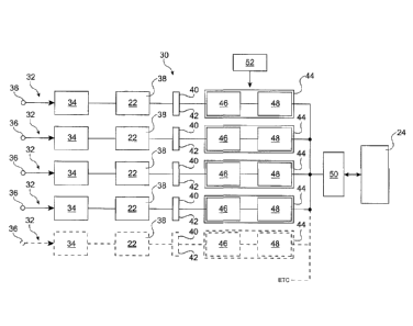
A sampling module according to a first
embodiment of the invention is designated generally by
the reference numeral 30.
The sampling module 30 includes a plurality of
input circuits 32, each input circuit 32 being for
sampling a particular analogue characteristic of a power
transmission system (not shown) to which the sampling
module 30 is electrically connected.
In the embodiment shown each input circuit 32
includes a scaling circuit 34 at an upstream, input end
36 thereof. The scaling circuit 34 is electrically
connected in series to an input of an analogue to
digital converter (ADC) 22. A preferred ADC 22, in the
form of a sigma-delta modulator 38, is shown.
An output of the sigma-delta modulator 38 is
electrically connected in series to an isolating circuit
40.
In other embodiments of the invention differing
series arrangements of the scaling circuit 34, ADC 22,
and isolating circuit 40 are also possible.
In each input circuit 32 the scaling circuit 34
is a resistor network (not shown) . The resistor network
may be in the form of a potential divider or a shunt,
for sampling analogue voltage and analogue current
characteristics, respectively.
Each isolating circuit 40 includes a single
pulse transformer 42, as detailed schematically in
Figure 4.
CA 02626569 2008-04-18
WO 2007/045682 PCT/EP2006/067594
9
A portion of each input circuit 32 downstream
from the isolating circuit 40 includes a digital signal
processing module 44, each of which includes digital
filter 46 and a re-sampling module 48.
The output of each digital signal processing
module 44 is electrically connected to a data interface
which, in turn, is connectable to a processing module
24.
The sampling module 30 also includes a control
interface 52 which is electrically connected to each
input circuit 32. The control interface 52 is configured
to be connectable to a control module (not shown), which
permits configuration of the digital signal processing
module 44 and the ADC 22.
In addition, the embodiment of the sampling
module 30 shown also includes a master clock 54 (Figure
3).
In use, each scaling circuit 34 scales a
respective sampled analogue characteristic to a level
suitable for analogue to digital conversion by the
corresponding sigma-delta modulator 38. It is possible
to determine the measurement range of each scaling
circuit 34 by selecting the values of the resistors
therein.
Furthermore, it is possible to improve the
accuracy of each sampled analogue characteristic by
calibrating each scaling circuit 34. Calibration could
correct any linear gain or offset errors introduced by a
given scaling circuit 34. Calibration could also correct
CA 02626569 2008-04-18
WO 2007/045682 PCT/EP2006/067594
any inversion of the sampled analogue characteristic
caused by incorrect assembly of the scaling circuit 34.
Each sigma-delta modulator 38 outputs a 1-bit,
serial, digital data stream corresponding to a given
5 sampled analogue characteristic. A clock signal controls
the sampling rate of each sigma-delta modulator 38.
Respective single pulse transformers 42 transfer
the digital data stream in a first direction from the
sigma-delta modulator 38 to a digital signal processor
10 44, while creating an electrical barrier between these
respective components. Each digital signal processor 44
may be configured to receive one or more digital data
streams.
Each single pulse transformer 42 also transfers
power to drive the corresponding sigma-delta modulator
38, and the aforementioned clock signal, in a second,
opposite direction.
Each single pulse transformer 42 implements a
forward converter topology with a frequency of operation
equal to that of the clock signal, thereby allowing the
corresponding sigma-delta modulator 38 to derive the
clock signal directly from the transferred power.
Transfer of the binary signal data stream is
achieved by changing the amplitude of the voltage used
to reset the transformer's flux, on a cycle by cycle
basis, from the secondary side of the forward converter.
Monitoring of the converter's primary waveform
determines whether a high voltage has been used to
quickly reset the flux or a low voltage has been used to
reset the flux more slowly.
CA 02626569 2008-04-18
WO 2007/045682 PCT/EP2006/067594
11
The digital filter 46 of each digital signal
processing module 44 filters a respective digital data
stream to, e.g. remove any extraneous noise.
The re-sampling module 48 of each digital signal
processing module 44 is able to generate a digital data
stream having a desired sampling rate.
Configuration of the digital signal processing
module 44 and the sampling rate of each sigma-delta
modulator 38 is conducted through the control interface
52, thereby allowing for differing sample rates and
filtering characteristics in each input circuit 32
according to the requirements of an attached processing
module 24, connected via the data interface 50.
Each input circuit 32 transmits its digital data
stream corresponding to a given sampled analogue
characteristic, to the processing module 24 via the data
interface 50. The master clock 54 time tags each digital
data stream so as to ensure that the data within a
particular stream is correctly synchronised following
transmission to the external device.
Accordingly, each input circuit 32 contributes
an independently filtered sample value to a given
digital data stream.
Each data stream block (44 in figure 3) accepts
the isolated bit streams from every input circuit (32 in
figure 3), filters them to remove unwanted frequency
components and then resamples them to produce packets of
samples at the sample rate required by the IED (24 in
figure 2) . The parameters of the digital filter (46 in
figure 3) and the period of the resampling logic (48 in
CA 02626569 2008-04-18
WO 2007/045682 PCT/EP2006/067594
12
figure 3) can both be configured by the IED (24), on-
the-fly if necessary, to suit the particular protection
algorithm. As the invention contains multiple concurrent
data stream blocks (44), it is possible to have
different protection algorithms running simultaneously
within the IED that require sample data at different
rates and with different levels of filtering.