Note: Descriptions are shown in the official language in which they were submitted.
CA 02626854 2008-04-22
WO 2007/056291 PCT/US2006/043204
PRINTED CIRCUIT BOARD STACKING
CONNECTOR WITH SEPARABLE INTERFACE
[0001] The present invention depicts electrical connectors for interconnection
to
printed circuit boards, and in particular for stacked board to board
interconnections.
[0002] It is common to provide interconnections to and from printed circuit
boards
to other devices and or to other printed circuit boards. It is also common
place to provide
multi-layer printed circuit boards in specific applications. For example, it
is common place
to provide multi-layer stacked printed circuit boards in such instances as
control technology
where the boards are stacked one above the other in parallel manner in a
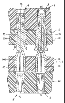
closely spaced
arrangement, with an insulator providing the insulative spacing between the
two printed
circuit boards. It is also common to provide printed circuit boards having a
like array of
plated through holes where the boards are interconnected at each plated
through hole by a
commoning connection at each of the plated through holes.
[0003] One such application has screw machined components having hexagonal,
(or
other multi-sided configuration) which are press-fit into one of the plated
through holes and
includes another pin or other interconnection device connected to the press-
fit screw
machined members. In such applications, the insertion forces for press fitting
the screw
machined components into the printed circuit board tend to be excessive and
cause the
screw machine contact and/or the printed circuit board to become damaged
during the
assembly.
[0004] These and other objects are to be accomplished with the following
embodiments and teachings.
[0005] According to the present invention, a board to board interconnect
assembly
is obtained comprising a stamped and formed socket contact having a compliant
portion for
interconnection to a first printed circuit board plated throughhole and an
integral socket
portion. A stamped and formed pin contact has a compliant portion for
interconnection to a
-1-
CA 02626854 2010-07-21
67789-578
second printed circuit board plated throughhole, and a pin portion for
interconnection to the integral socket portion.
[0006] A board to board interconnect assembly, comprises first and second
printed circuit boards positioned in a spaced apart and parallel manner, each
printed circuit board having an array of plated throughholes, with the arrays
in
each board being in alignment. A stamped and formed socket contact has an
integral socket portion and a compliant portion interconnected to the first
printed
circuit board plated throughhole. A stamped and formed pin contact has an
integral pin portion and a compliant portion interconnected to a second
printed
circuit board plated throughhole. The pin portion projects through the first
printed
circuit board, and through the socket compliant portion, to interconnect the
pin
portion and socket portion.
In one broad aspect of the present invention, there is provided a
board to board interconnect assembly, comprising: first and second printed
circuit
boards positioned in a spaced apart and parallel manner, each printed circuit
board having an array of plated throughholes, with said arrays in each board
being
in alignment; a stamped and formed socket contact having an integral socket
portion and a compliant portion interconnected to said first printed circuit
board
plated throughhole; a stamped and formed pin contact having an integral pin
portion and a compliant portion interconnected to a second printed circuit
board
plated throughhole; and said pin portion projecting through said first printed
circuit
board, and through said compliant portion of said socket contact, to
interconnect
said pin portion and socket portion.
[0007] Figure 1 is a side view of the components of the board to board
interconnect of the invention shown in a space apart manner and poised for
interconnection with each other;
[0008] Figure 2 shows an underside perspective view of the socket
assembly of Figure 1;
-2-
CA 02626854 2010-07-21
67789-578
[0009] Figure 3 shows a perspective view similar to that of Figure 2, of the
housing without the socket contacts;
[0010] Figure 4 is an enlarged view of the portion denoted in Figure 3;
[0011] Figure 5 is a cross-sectional view through lines 5-5 of Figure 4;
[0012] Figure 6 is a perspective view of the socket contact of the present
invention;
[0013] Figure 7 is an enlarged view of the portion denoted in Figure 1;
[0014] Figure 8 is an underside perspective of the pin assembly shown in
Figure 1;
[0015] Figure 9 is a perspective view of one of the pin contacts of Figure 8;
-2a-
CA 02626854 2008-04-22
WO 2007/056291 PCT/US2006/043204
[0016] Figure 10 is an enlarged view of the portion denoted in Figure 1; and
[0017] Figure 11 is a cross-sectional view similar to that of Figure 1 showing
the
board to board inner connect in its fully mated condition.
[0018] With reference first to Figure 1, a board to board interconnect
assembly is
shown generally at 2 which includes a socket assembly 4, having a socket
housing 6 and a
plurality of socket terminals 8. The socket assembly 6 is shown poised for
receipt and
interconnection to, a printed circuit board 10. Assembly 2 further includes a
pin assembly
12 including a pin housing 14 and a plurality of pin terminals 16. Pin
assembly 12 is
shown poised for receipt and interconnection to a printed circuit board 18.
[0019] With reference now to Figure 2, socket assembly 4 is shown in greater
detail
as including a plurality of columns and rows of socket terminals 8 defining an
array of
socket terminals. With reference to Figures 3 and 4, socket housing 6 is shown
in greater
detail where socket housing 6 is comprised an insulative plate member 20
having a plurality
of openings at 22. As shown in Figure 4, openings 22 include a U-shaped
portion at 24
and a flat sidewall portion 26. As shown in Figure 3-5, openings 22 extend
between an
internal face 28 and an external face 30.
[0020] With reference now to Figure 6, socket terminals 8 are shown including
compliant portions 32 integrally connected to socket portions 34 by way of an
integral strap
36. As shown, compliant portions 32 include a C-shaped cross section around a
body
portion 38 which necks down into lead in portions 40 as described herein. As
also shown
in Figure 6, body portion 38 of compliant portion 32 includes an upper
engaging surface 42
as will be described herein. Socket portion 34 includes a C-shaped retaining
portion 46
having socket beams 50 extending downwardly from the retaining portion 46. As
shown
socket beams are deflected inwardly to form a constricted portion between
contact surfaces
52 of socket beams 50 and with a contact surface portion 54 of strap 36.
[0021] Thus socket terminals 8 may be positioned in openings 22 with retaining
portions 46 being positioned in openings 22, and with the socket beams 50
depending
-3-
CA 02626854 2008-04-22
WO 2007/056291 PCT/US2006/043204
downwardly as shown in Figure 7. As also shown, body portion 38 is a larger
diameter
than opening 22 and thus engaging surface 42 abuts inner face 28 of socket
housing 6.
[0022] With respect now to Figure 8, pin assembly 12 is shown with a plurality
of
pin terminals 16 positioned in a plurality of columns and rows defining an
array of pin
terminals 16. It should be appreciated that the arrays of the pin terminals 16
and the array
of socket terminals 8 are substantially identical in order to provide mating
engagement
between the two. It should also be appreciated that pin housing 14 is
substantially identical
to socket housing 6, and therefore pin housing 14 will not be described in
detail herein.
[0023] With respect now to Figure 9, pin terminals 16 will now be described.
Pin
terminals 16 includes compliant portion 60 having a socket portion 62
integrally attached by
way of strap portion 64. Furthermore pin portion 66 is integrally attached to
compliant
portion 60 from the opposite end as the socket portion 62. Socket portion 62
includes a C-
shaped retaining portion 68 in the way of a compliant C-shaped member, having
socket
beams 70 extending downwardly therefrom. Socket portion 62 defines a three
point contact
by way of contact surfaces 72 of socket beams 70, and by way of contact
surface portion 74
on strap portion 64. Furthermore, compliant portion 60 includes a body portion
80 of C-
shaped configuration on the cross section together with a lead in portion at
82, and an
engaging portion at 84.
[0024] Thus, as shown in Figure 10, pin terminals 16 are situated in pin
housing 14
with the C-shaped retaining portions 68 maintaining the pin terminals 16 in
openings 22
with the compliant portion 60 and the pin portion 66 exterior to pin housing
14, and with
the engaging surface 84 in abutment with internal face 28. Thus, it is the
socket assembly
4 in the configuration of Figure 7 and the pin assembly 12 in the
configuration of Figure 10
which allow for the interconnection of the two assemblies 4, 12 and the two
printed circuit
boards 10 and 18 to be interconnected together. As shown in Figure 1, printed
circuit
board 10 includes a plurality of plated through holes 100 (only one of which
is shown)
however it should be appreciated that the through holes 100 have a like array
as the array
of socket terminals 8. Furthermore circuit board 18 is shown poised over pin
assembly 12
where printed circuit board 18 has a plurality of plated through holes 102
(only one of
-4-
CA 02626854 2008-04-22
WO 2007/056291 PCT/US2006/043204
which is shown) for interconnection to pin assembly 12. Figure 1 also shows
multiple
spacers such as 104 positioned between the two circuit boards 10, 18. These
spacers are
intended to insulate the two boards 10, 18 and their components from each
other. While
shown as washers or grommets, it should be appreciated that this insulation
could also be in
the form of a sheet gasket, or any other spacer.
[0025] To make the interconnection, one of the boards 10 or 18 is positioned
over
its respective assembly 4 or 12. For example, and with respect again to Figure
1, printed
circuit board 10 is positioned with the plurality of plated through holes 100
to be positioned
over the compliant portions 32 which retains and electrically connects the
socket terminals
8 to the plated through holes 100. During insertion into the PCB, the lead-in
portions (40)
of the socket contact flare open to allow for ease of mating to pin (66).
Meanwhile printed
circuit board 18 can be positioned with the plated through holes over pins 66
and in
interconnection with compliant portions 60 which causes pins 66 to project out
of plated
through holes 102. As shown in Figure 11, the two assemblies may now be
brought
together, such that pins 66 protrude into openings 44 (Figure 7) of the socket
terminals 8
and the pin portions 66 extends upwardly through compliant portion 32, to make
contact
with socket beams 50 and the kinked contact surface 54 (Figure 6).
[0026] Thus, a very inexpensive interconnect has been provided, for the
placement
of two printed circuit boards in a back to back manner for interconnecting the
two boards
together. It should also be appreciated from Figure 1, 10 or 11 that a further
interconnection could be made with the socket beams 70 of pin terminal 16 for
further
electrical interconnection.
-5-