Note: Descriptions are shown in the official language in which they were submitted.
CA 02627061 2010-11-04
WO 2007/097811 PCT/1JS2006/060154
CAPACITOR STRAP
SPECIFICATION
BACKGROUND OF THE INVENTION
1. FIELD OF INVENTION
The current invention relates to security tags and more particulary, discloses
a capacitor
strap that can be applied to an EAS or RFID coil or antenna to complete the
EAS or RFID tag.
2. DESCRIPTION OF RELATED ART
Electronic article surveillance (EAS) security tags, typically comprise a
resonant circuit
that utilize at least one coil and at least one capacitor that operate to
resonate when exposed to a
predetermined electromagnetic field (e.g., 8.2 MHz) to which the EAS tag is
exposed. By way of
example only, the coil and the capacitor are etched on a substrate whereby a
multi-turn conductive
trace (thereby forming the coil) terminates in a conductive trace pad which
forms one plate of the
capacitor. On the opposite side of the substrate another conductive trace pad
is etched to form the
second capacitor plate, while an electrical connection is made through the
substrate from this
second plate to the other end of the coil on the first side of the substrate;
the non-conductive
substrate then acts as a dielectric between the two conductive trace pads to
form the capacitor.
Thus, a resonant circuit is formed. Various different resonant tag products
are commercially
available and described in issued patents, for example, U.S. Pat. Nos.
5,172,461; 5,108,822;
4,835,524; 4,658,264; and 4,567,473 all describe and disclose electrical
surveillance tag
structures. However, such products utilize, and indeed require, substrates
which use patterned
sides of conductive material on both face surfaces of the substrate for proper
operation. Special
conductive structures and manufacturing techniques must be utilized on both
substrate faces for
producing such resonant tag products. Currently available EAS tag structures
have numerous
drawbacks. For example, since special patterning and etching techniques must
be utilized on both
sides of the available tags to produce the proper circuit, per unit processing
time and costs are
increased. Furthermore, the complexity of the manufacturing machinery required
for production is
also increased. Oftentimes, complex photo-etching processes are used to form
the circuit
structures. As may be appreciated, two sided photo-etching is generally time
consuming and
1
CA 02627061 2010-11-04
WO 2007/097811 PCT/US2006/060154
requires precise alignment of the patterns on both sides. Additional material
is also necessary to
pattern both sides, thus increasing the per unit material costs.
With particular regard to radio frequency identification (REID) tags, RFID
tags include an
integrated circuit (IC) coupled to a resonant circuit as mentioned previously
or coupled to an
antenna (e.g., a dipole) which emits an information signal in response to a
predetermined
electromagnetic field (e.g., 13.56 MHz). Recently, the attachment of the IC
has been
accomplished by electrically-coupling conductive flanges to respective IC
contacts to form a "chip
strap." This chip strap is then electrically coupled to the resonant circuit
or antenna. See for
example U.S. Patent Nos. 6,940,408 (Ferguson, et al.); 6,665,193 (Chung, et
a).); 6,181,287
(Beigel); and 6,100,804 (Brady, et al.).
However, it has been determined that the formation of the capacitive element
of the EAS
circuit or of the RFID circuit is what substantively controls the tuning of
the EAS resonant circuit,
or the RFID circuit, to respond properly to the desired electromagnetic field.
Thus, there remains
a need for an EAS or RFID tag that can be efficiently formed and tuned
properly, as well as a
method for efficiently and accurately forming, as well as controlling the
tuning of, an EAS tag or
an RFID tag.
BRIEF SUMMARY OF THE INVENTION
A strap component for electrically bridging at least two respective portions
of an antenna
or coil component of an EAS or RFII) tag or inlay. The strap component is a
thin, generally
planar member comprising a first electrically conductive planar element, a
second planar
electrically conductive element and a planar dielectric layer disposed between
at least portions of
the first and second electrically conductive planar elements, whereupon the
strap component
exhibits a desired capacitance. The first electrically conductive element
includes a first portion
arranged to be secured in electrical continuity with one of the at least two
respective portions of
the antenna or coil. The second electrically conductive element includes a
first portion arranged to
be secured in electrical continuity with another of the at least two
respective portions of the
antenna or coil.
An EAS or RFID tag or inlay comprising an antenna or coil component and a
strap
component bridging at least two respective portions of the antenna or coil
component. The strap
component is a thin, generally planar member comprising a first electrically
conductive planar
element, a second electrically conductive planar element and a planar
dielectric layer disposed
2
CA 02627061 2008-04-23
WO 2007/097811 PCT/US2006/060154
between at least portions of the first and second electrically conductive
planar elements,
whereupon the strap component exhibits a desired capacitance. The first
electrically conductive
element includes a first portion secured in electrical continuity with one of
the at least two
respective portions of the antenna or coil. The second electrically conductive
element includes a
first portion secured in electrical continuity with another of the at least
two respective portions of
the antenna or coil.
A thin, generally planar, flexible, strap component for electrically bridging
at least two
respective portions of an antenna or coil component of an EAS or RFID tag or
inlay. The strap
component exhibits a desired capacitance and comprises a first electrically
conductive planar
element and a second electrically conductive planar element, and a planar
dielectric layer disposed
between at least portions of the first and second electrically conductive
planar elements. The first
electrically conductive element includes a first portion arranged to be
secured in electrical
continuity with one of the at least two respective portions of the antenna or
coil. The second
electrically conductive element includes a first portion arranged to be
secured in electrical
continuity with another of the at least two respective portions of the antenna
or coil, resulting in
the formation of the EAS or RFID tag or inlay.
A method of making an EAS or RFID tag or inlay comprising: (a) providing a
thin,
generally planar antenna or coil component; (b) providing a thin, generally
planar, strap
component comprising a first electrically conductive planar element, a second
electrically
conductive planar element and a planar dielectric layer disposed between at
least portions of the
first and second electrically conductive elements, and whereupon the strap
component exhibits a
desired capacitance; and (c) causing the strap component to bridge at least
two respective portions
of the antenna or coil component, whereupon a first portion of the first
electrically conductive
element is secured in electrical continuity with one of the at least two
respective portions of the
antenna or coil and a first portion of the second electrically conductive
element is secured in
electrical continuity with another of the at least two respective portions of
said antenna or coil.
BRIEF DESCRIPTION OF SEVERAL VIEWS OF THE DRAWINGS
The invention will be described in conjunction with the following drawings in
which like
reference numerals designate like elements and wherein:
Fig. I is a plan view of a capacitor strap of the present invention;
Fig. 2 is a cross-sectional view of the capacitor strap taken along line 2-2
of Fig. 1;
3
CA 02627061 2008-04-23
WO 2007/097811 PCT/US2006/060154
Fig. 2A is a cross-sectional view of the capacitor strap taken along line 2-2
of Fig. 1
formed by a hybrid-style process;
Fig. 2B is a cross-sectional view of the capacitor strap taken along line 2-2
of Fig. I
formed by an etching process and including an insulator layer along the lower
conductive layer;
Fig. 3 is a plan view of a second embodiment of the capacitor strap which
includes an
integrated circuit electrically-coupled to the capacitor strap;
Fig. 4 is a cross-sectional view of the capacitor strap of Fig. 3 taken along
line 4-4 of Fig.
3;
Fig. 5 is a plan view of the capacitor strap of Fig. I applied to a multi-turn
coil;
Fig. 5A is an equivalent circuit schematic of the circuit formed in Fig. 5;
Fig. 6 is a cross-sectional view of the tag of Fig. 5 taken along line 6-6 of
Fig. 5;
Fig. 7 is a plan view of the capacitor strap of Fig. 3 applied to a multi-turn
coil;
Fig. 7A is an equivalent circuit schematic of the circuit formed in Fig. 7;
Fig. 8 is a cross-sectional view of the tag of Fig. 7 taken along line 8-8 of
Fig. 7;
Fig. 9 is a plan view of a plan view of a capacitor strap of Fig. 3, and a
chip strap applied
in parallel to a multi-turn coil;
Fig. 9A is an equivalent circuit schematic of the circuit formed in Fig. 9;
Fig. 10 is a cross-sectional view of the tag of Fig. 9 taken along line 10-10
of Fig. 9;
Fig. 11 is a cross-sectional view of the tag of Fig. 9 taken along line 11-11
of Fig. 9;
Fig. 12 is a plan view of an integrated parallel chip-capacitor strap applied
to a multi-turn
coil;
Fig. 12A is a plan view of only the integrated parallel chip-capacitor strap
of Fig. 12;
Fig. 13 is a cross-sectional view of the tag of Fig. 12 taken along line 13-13
of Fig. 12;
Fig. 14 is a cross-sectional view of the tag of Fig. 12 taken along line 14-14
of Fig. 12;
Fig. 15 depicts the creation process of a metal (e.g., aluminum) laminate in
making
capacitor straps;
Fig. 16 depicts a printing photoresist image process on the metal laminate
created in Fig.
15;
Fig. 17 depicts an etching process for creating the capacitor straps out of
the metal
laminate upon which the photoresist was applied in Fig. 16;
4
CA 02627061 2008-04-23
WO 2007/097811 PCT/US2006/060154
Fig. 18 depicts the application or a removable liner to the capacitor strap
web and the
removal of waste therefrom, resulting in a roll of capacitor straps ready for
application to a coil or
antenna;
Fig. 19 depicts a portion of the "hybrid-style" process of forming capacitor
straps and
more particularly shows the creation of a metal (e.g., aluminum) laminate
formed from a double-
side heat seal coated metal (e.g., aluminum) laminate;
Fig. 20 depicts the creation of a second double-side heat seal coated metal
(e.g.,
aluminum) laminate using the "hybrid-style" process; and
Fig. 21 depicts the combination of these two metal (e.g., aluminum) laminates
shown in
Figs. 19-20, along with the application of a releasable liner, and waste
removal, resulting in a roll
of capacitor straps ready for application to a coil or antenna.
DETAILED DESCRIPTION OF THE INVENTION
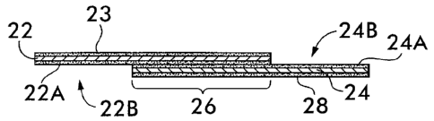
Fig. I depicts an enlarged plan view of a capacitor strap 20 of the present
invention. As
can be seen most clearly in Fig. 2, the capacitor strap 20 is a thin film
capacitor, and may be
flexible, that comprises a first electrically conductive planar element 22
having an associated
dielectric layer 22A and a second electrically conductive planar element 24
having an associated
dielectric layer 24A and wherein portions of the elements 22 and 24 overlap
26, thereby forming a
capacitor. As is known to those skilled in the art, the amount of overlap 26
determines the
capacitance.
Although there are many ways of forming the capacitor strap 20, the preferred
method is to
provide a pair of rolls, each containing a, metal foil (e.g., aluminum) that
is heat fused to a
dielectric material (e.g., a heat seal dielectric material such as polyester
or polyethylene which
readily bonds to aluminum; however, other dielectric materials, such as a
styrene-acylate polymer
or a vinyl acetate could also be used; and/or the dielectric layer may form a
coating applied to the
metal foil). These rolls are oriented such that during formation of the
capacitor straps 20, the
associated dielectric layers 22A/24A face each other. The associated
dielectric layers 22A/24A are
then heat fused together. Using a cutting die (not shown) and by precisely
controlling the cut of
the first electrically conductive planar element 22 and its associated
dielectric layer 22A (or vice
versa, i.e., cutting the second electrically conductive planar element 24 and
its associated
dielectric layer 24A), large numbers of capacitor straps 20 can be generated.
By also varying the
relative lengths of the element 22/associated dielectric layer 22A and the
element 24/associated
dielectric layer 24A (i.e., varying the overlap 26), capacitor straps 20 of
different capacitances can
CA 02627061 2008-04-23
WO 2007/097811 PCT/US2006/060154
also be generated. Alternatively, the metal foil may be purchased with the
dielectric layer already
applied (known as a "hybrid-style" (see Figs. 19-21 and their related
discussion below)). Or, the
dielectric layer may be applied to the metal foil by printing the dielectric
on-line using a gravure
knife over roll or a similar printing process (e.g., as part of an etching
process, see Figs. 15-18 and
their related discussion below).
A capacitor strap 20 is then electrically coupled to an EAS or RFID coil or
antenna, by
electrically connecting the non-overlapping ends 22B of the first electrically
conductive planar
element 22 and the non-overlapping end 24B of the second electrically
conductive planar element
24 to respective portions of the coil or antenna. Although there are many ways
of achieving such
an electrical connection 25 (which are indicated by solid black circular dots
in the figure), a
preferred way is a "cold weld" using high pressure whereby the planar elements
22/24 are
electrically coupled to the respective portions of the coil; an alternative
way is by "hot welding"
the planar elements to the respective portions of the coil; this involves
heating the conductive
portions and then crimping them such there is metal-to-metal contact of the
planar element 22 (or
24) to the respective coil portion, thereby forming the electrical connection.
Where the coil or
antenna comprises several turns, for example as shown by the coil 10 in Fig.
5, in order to prevent
shorting of the second electrically conductive planar element 24, an insulator
layer 28 (Fig. 2A,
e.g., a dielectric material), or paper insulator layer 28A (Fig. 2B), is
applied to the element 24, or
is otherwise interposed between the second electrically conductive planer
layer 28 and the
coil/antenna. As can be most clearly seen in Fig. 6, the insulator layer 28
isolates the element 24
from turn tracks 13 and 14, while electrical connection of the capacitor strap
20 is made at
connections 25A and 25B at ends 22B and 24B of the capacitor strap 20 to coil
tracks 11 and 12,
respectively. It should be noted that where a coil of less than one turn is
provided, the insulator
layer 28 is not required since the capacitor strap 20 does not crossover any
other coil tracks. Thus,
an EAS tag or inlay 16 is created having an equivalent circuit formed by the
coil 10 and the
capacitor strap 20, as shown in Fig. 5A.
It should be noted that the coil 10 is formed as part of a conductive layer
that is on or in a
substrate which is not shown.
As mentioned earlier, Figs. 2A and 2B provide alternative insulator layer
schemes. The
preferred method, as discussed with respect to Figs. 19-21, utilizes combining
a pair of double
side heat seal coated metal (e.g., aluminum) to form the capacitor straps 20.
In particular, as
shown in Fig. 2A, a first laminate formed from the first electrically
conductive planar element 22
6
CA 02627061 2008-04-23
WO 2007/097811 PCT/US2006/060154
covered on respective sides with insulator layers 23 and 22A is combined with
a second laminate
formed from the second electrically conductive planar element 24 covered on
respective sides
with insulator layers 24A and 28; these two double side heat seal coated metal
layers are
combined at the interface between insulative layers 22A and 24A to form the
capacitor strap 20.
A less preferred method does not use a double heat seal coated metal (e.g.,
the process shown in
Figs. 15-18) in which case a separate insulative layer 28A may be applied to
the exposed side of
the second electrically conductive planar element 24 to prevent electrical
shorting when the
capacitor strap 20 is applied to the coil/antenna where the exposed side of
the element 24 may
cross over coil/antenna conductors.
Fig. 3 depicts a plan view of a capacitor strap 120 which includes an IC that
is in series
with the capacitor. In particular, the capacitor strap 120 comprises a similar
configuration as
described previously with the capacitor strap 20. However, in addition, the
element 22 of the non-
overlapping end 22B is electrically coupled to an electrical contact (not
shown) of an IC 15. The
other electrical contact (also not shown) of the IC 15 is electrically coupled
to a flange 122B that
is similar to the construction of the non-overlapping end 22B. As can be seen
most clearly in Fig.
4, there is a gap G that separates the element 22 of the non-overlapping end
22B and the flange
122B. This prevents shorting of the IC 15 contacts.
This capacitor strap 120 can then be applied to a coil 10, as shown in Fig. 7
to form an
RFID tag or inlay 17. In particular, by electrically connecting the non-
overlapping end 24B of the
second electrically conductive planar element 24 and the flange 122B to
respective portions of the
coil or antenna. As shown in Figs. 7-8, the non-overlapping edge 24B is
electrically connected at
25A to turn track 11 and the flange 122B is electrically coupled at 25B to
turn track 12. The
insulative layer 28 under the element 24 prevents any shorting to turn tracks
13-14 of the coil 10.
An equivalent circuit of the RFID tag 17 is shown in Fig. 7A, showing the
series relationship of
the IC 15 and the capacitor and the coil 10.
It should be noted that the actual capacitor formed in Figs. 4 and 7 by the
capacitor strap
120 is similar in construction to that in capacitor strap 20. However, it
should be noted that the
actual capacitor formed has a different capacitance value than the capacitor
formed in the
capacitor strap 20 because RFID operation is, by way of example only, 13.56
MHz as compared to
EAS operation which is approximately 8.2 MHz.
7
CA 02627061 2008-04-23
WO 2007/097811 PCT/US2006/060154
It should be readily apparent from these two examples, that depending on the
type of
capacitor strap applied to the coil 10, either capacitor strap 20 or capacitor
strap 120, an EAS tag
or an RFID tag, respectively, is formed.
It should be understood that the capacitor straps 20 and 120 can be
manufactured with
varying amounts of overlap 26 (for different capacitance values) and with
varying lengths of the
non-overlapping edges 22B, 24B and flange 122B such that the capacitor straps
20, 120 can be
applied over different coil tracks of the coil 10 to change the resonant
frequency of the tag 16 and
17. Thus, the relative position of the capacitor straps 20 and 120 shown with
respect to the coil 10
are by way of example only.
Figs. 9-11 depict the use of the capacitor strap 20 and a conventional chip
strap 19 being
used on a common coil l0A to form an RFID tag 18 using a parallel resonant
circuit, as shown in
Fig. 9A. The capacitor strap 20 is electrically coupled to the coil in a
manner similarly discussed
with regard to Figs. 5-6 previously and will not be discussed again. The chip
strap 19 comprises
an IC 15 that is electrically connected to conductive flanges 19A and 19B. A
gap 19G also
separates these two flanges to prevent shorting the IC 15 electrical contacts
(not shown). The
conductive flanges 19A and 19B are electrically coupled to respective
locations of the coil l0A at
connections 25C and 25D, respectively. To prevent shorting the IC 15 when it
is electrically
coupled to the coil 10A, an insulating layer 19C (e.g., paper) is disposed
between the conductive
flanges 19A/19B and the coil 10A, as shown most clearly in Fig. 10. It should
be understood that
the chip strap 19 does not comprise a thin film capacitor as does the
capacitor strap 20 (or
capacitor strap 120).
Figs. 12-14 depict an RFID tag 18' using a parallel resonant circuit (similar
to the one
shown in Fig. 9A) but with an integrated parallel chip-capacitor strap 220;
thus, instead of using a
separate capacitor strap 20 and a conventional chip strap 19, the integrated
parallel chip-capacitor
strap 220 is used. In particular, as shown most clearly in Fig. 12A, the
integrated parallel chip-
capacitor strap 220 is formed from basically three parts: a rectangular
conductive flange 222, an
"L-shaped" conductive flange 224 having a narrow section 226 that overlaps a
portion of the
rectangular conductive flange 222, and an IC 15. The IC 15 has respective
electrical contacts (not
shown) that are electrically coupled to the flange 222 and to the flange 224.
A gap G separates the
flanges 222 and 224 from electrically shorting out the contacts. A dielectric
layer 226A is
disposed between the flange 222 and the narrow section 226 which forms the
capacitor. A
dielectric layer 222A electrically insulates the rectangular conductive flange
222 from the turn
8
CA 02627061 2010-11-04
WO 2007/097811 PCT/US2006/060154
tracks 11-14. The flange 222 is electrically coupled to the coil track 11 at
connection point 25A as
shown in Figs. 12 and 13. The L-shaped conductive flange 224 is electrically
coupled to the coil
track 12 at connection point 25B as also shown in Figs. 12 and 13. As
described earlier with
respect to varying the capacitance value of the capacitor straps 20 and 120,
the capacitor strap 220
can be manufactured with varying amounts of overlap of the narrow section 226
with respect to
the flange 222 to provide capacitor straps 220 with different capacitance
values.
It should be noted that the use of the capacitor straps 20, 120 and 220 are
not limited to
coils. These straps could also be used in higher frequency applications where
antennas, such as
dipoles are used. Thus, by way of example only, a capacitor strap 20 or 120 or
220 could be
positioned between the dipole elements of a dipole antenna to form a tag
operating in the UHF or
microwave frequency bands.
It should also be noted that although all of the capacitor straps 20, 120 and
220 are shown
being electrically coupled on top of the coils 10/10A, this is by way of
example only. These straps
can also be electrically coupled below the coils 10/10A or antenna. If so,
penetration of the
substrate (not shown) which supports the coil or antenna would have to occur
to permit the
electrical connection.
The term "inlay" as used throughout this Specification means that the
completed tag (e.g.,
EAS tag 16, RFID tags 17, or 18 or 18') may themselves either form a portion
of a label or be
coupled to a label for use on, or otherwise associated with, an item.
The capacitor straps 20,120 and 220 can also include deactivation mechanisms
that permit
the security tag formed thereby to be deactivated by an external field when
required such as
including a predetermined breakdown voltage of the capacitor strap, or
including a breakdown in a
specific area of the capacitor strap, such as disclosed in U.S. Patent Nos.
5,861,809 (Eckstein, et
al.); 6,232,878 (Rubin) and 6,025,780 (Bowers, et al.).
As mentioned earlier, Figs. 15-18 depict the creation of a roll of capacitor
straps using a
printing/etching process.
For clarity, throughout Figs. 15-18, cross-sections of portions of layers or
laminates are
shown at the different stages. It should be noted that these thicknesses are
greatly exaggerated and
do not depict the actual thickness of the various layers.
In particular, a laminate 408 is formed from two layers of a metal (e.g.,
aluminum) 400 and
402 (from respective rolls 400A/402A) that are joined to a polyethylene (PET)
extrusion 404 (a
9
CA 02627061 2008-04-23
WO 2007/097811 PCT/US2006/060154
"hot" PET) from a PET extrusion stage 404A. Following the combining stage 406,
the metal
laminate 408 is wound on a take-up roll 410. Next, as shown in Fig. 16, the
take-up roll 410 is fed
to a printing process whereby photoresist is selectively applied, on both
sides, at a printing station
412 and the "printed laminate" 414 is fed to a take-up roll 414A. As shown in
Fig. 17, the printed
laminate 414 is then fed to an etching process 416 whereby portions of the
metal (e.g., aluminum)
layers, on both sides of the laminate 414, are etched away, thereby leaving
isolated portions of
metal bands on both sides of the laminate, thereby forming a capacitor strap
web 418. This
capacitor strap web 418 is then fed to a take-up roll 420. The next stage
(Fig. 18) in the process is
to apply all of these capacitor straps to a liner with a releasable adhesive
and then to physically
separate each capacitor strap 20 from adjacent straps. In particular, a roll
422A of a liner 422 with
a releasable adhesive is combined with the capacitor strap web 418 at station
424. Then, at a die
cutting station 426, portions of the extrusion layer 404 in between the
capacitor straps 20 are
severed and removed to a waste take-up roll 428. The end result is a plurality
of capacitor straps
20 (or 120 or 220) on a web 430 that are wound up on a roll 430A that are
ready for application to
coils or antennas.
As also mentioned earlier, an alternative process for making capacitor straps
uses the
"hybrid-style" process. One of the advantages of this process is that the
metal layers used in this
process are heat seal coated. As a result, the capacitor "plates" of the
capacitor straps are
insulated from the beginning so there is no need to introduce a separate
insulating layer 28A, as
shown in Fig. 2B, when the capacitor strap may span several turns of a coil or
antenna. Figs. 19-
21 depict the creation of a roll of capacitor straps using the "hybrid-style"
process.
For clarity, throughout Figs. 19-21, cross-sections of portions of layers or
laminates are
shown at the different stages. It should be noted that these thicknesses are
greatly exaggerated and
do not depict the actual thickness of the various layers.
In particular, as shown in Fig. 19, a liner 500 from a liner supply roll 500A
is fed to an
extruder 502A where an adhesive 502 is applied to the liner 500 to form a
liner 504 with a
releasable adhesive. From a supply roll 506A of double side heat seal coated
metal (e.g.,
aluminum) 506, the heat seal coated metal 506 is combined, at combining
station 507, with the
liner 504 with the releasable adhesive to form a laminate 508 that forms a
"set of plates" of the
capacitor straps; a take-up roll 508A holds this laminate 508. A second
similar laminate 608 is
formed using a similar process. This second similar laminate 608 forms the
"other set of plates" of
the capacitor straps. Reference numbers 600-608A correspond directly to
reference numbers 500-
CA 02627061 2008-04-23
WO 2007/097811 PCT/US2006/060154
508A and are therefore not discussed any further. The take-up rolls 508A and
608A are then used
in a combination process to form the capacitor straps, as shown in Fig. 21. In
particular, the
laminates 508 and 608 are die cut at respective die cutting stations 510 and
610 through the
double side heat seal coated metal portions (506 and 606) and the waste
removed onto respective
waste take-up rolls 511/611 in order to form isolated bands 512/612 of the
double heat seal coated
metal (e.g., aluminum). As can be seen in Fig. 21, these isolated bands 512
and 612 are facing
each other (e.g., bands 512 face downward and bands 612 face upward). In these
orientations, the
individual isolated bands 512 and 612 are registered and then stamped at
stamping station 514 to
form the capacitor straps. To permit the individual capacitor straps to be
removed and applied to
coils or antennas, one of the liners with the releasable adhesive (i.e., 504
or 604) needs to be
removed onto a take-up roll 700. The end result is a plurality of capacitor
straps 20 (or 120 or 220)
on web 702 that are wound up on a roll 702A that are ready for application to
coils or antennas.
Fig. 21 also shows the capacitor strap 20 in cross section that corresponds to
Fig. 2A.
While the invention has been described in detail and with reference to
specific examples
thereof, it will be apparent to one skilled in the art that various changes
and modifications can be
made therein without departing from the spirit and scope thereof.
11