Note: Descriptions are shown in the official language in which they were submitted.
CA 02627439 2008-04-25
WO 2007/056081 PCT/US2006/042849
1
APPARATUS AND METHOD FOR TRANSMIT POWER CONTROL FREQUENCY
SELECTION IN WIRELESS NETWORKS
BACKGROUND OF THE INVENTION
[0001] The present invention generally relates to communications systems and,
more
particularly, to wireless systems, e.g., terrestrial broadcast, cellular,
Wireless-Fidelity (Wi-
Fi), satellite, etc.
[0002] A Wireless Regional Area Network (WRAN) system is being studied in the
IEEE
802.22 standard group. The WRAN system is intended to make use of unused
television (TV)
broadcast channels in the TV spectrum, on a non-interfering basis, to address,
as a primary
objective, rural and remote areas and low population density underserved
markets with
performance levels similar to those of broadband access technologies serving
urban and suburban
areas. In addition, the WRAN system may also be able to scale to serve denser
population
areas where spectrum is available.
SUMMARY OF THE INVENTION
[0003] As noted above, one goal of the WRAN system is not to interfere with
existing
incumbent signals, such as TV broadcasts. As such, a WRAN endpoint uses a
channel that
does not have an incumbent TV signal present. However, even if the channel is
clear of a
TV signal - a TV signal may be present on an adjacent channel. As such, the
transmission
signal from the WRAN endpoint may still interfere with the adjacent TV signal
by
introducing non-linear effects (e.g., cross-modulation products). In this
regard, a wireless
endpoint performs transmit power control (TPC) to avoid interfering with a TV
broadcast on
an adjacent channel. In particular, and in accordance with the principles of
the invention, a
wireless endpoint transmits a signal on a channel; and adjusts a power level
of the
transmitted signal upon detection of a signal on an adjacent channel.
[0004] In an illustrative embodiment of the invention, a wireless endpoint is
a Wireless
Regional Area Network (WRAN) endpoint, such as a base station (BS) or customer
premise
equipment (CPE). The WRAN endpoint performs channel sensing to determine which
channels are available for use and begins transmission on an available
channel. Upon
detection of a TV broadcast on an adjacent channel, the WRAN endpoint adjusts
a power
level of its transmitted signal.
CA 02627439 2008-04-25
WO 2007/056081 PCT/US2006/042849
2
[0005] In view of the above, and as will be apparent from reading the detailed
description, other embodiments and features are also possible and fall within
the principles
of the invention.
BRIEF DESCRIPTION OF THE DRAWINGS
[0006] FIG. 1 shows Table One, which lists television (TV) channels;
[0007] FIGs. 2 and 3 show Tables Two and Three, which list frequency offsets
under
different conditions for a received ATSC signal;
[0008] FIG. 4 shows an illustrative WRAN system in accordance with the
principles of
the invention;
[0009] FIG. 5 shows an illustrative receiver for use in the WRAN system of
FIG. 4 in
accordance with the principles of the invention;
[0010] FIG. 6 shows an illustrative flow chart for use in the WRAN system of
FIG. 4 in
accordance with the principles of the invention;
[0011] FIGs. 7 and 8 illustrate tuner 305 and carrier tracking loop 315 of
FIG. 5;
[0012] FIGs. 9 and 10 show a format for an ATSC DTV signal;
[0013] FIGs. 11-21 show various embodiments of ATSC signal detectors;
[0014] FIG. 22 shows an illustrative flow chart for use in the WRAN system of
FIG. 4 in
accordance with the principles of the invention;
[0015] FIG. 23 shows an illustrative OFDM modulator in accordance with the
principles
of the invention;
[0016] FIG. 24 shows an illustrative message flow for use in the WRAN system
of FIG.
4;
[0017] FIG. 25 shows an illustrative TPC report for use in the WRAN system of
FIG. 4;
[0018] FIG. 26 shows another illustrative message flow for use in the WRAN
systein of
FIG.4;
[0019] FIG. 27 shows an illustrative OFDMA frame for use in the WRAN systei-n
of
FIG. 4; and
[0020] FIG. 28 shows another illustrative receiver for use in the WRAN system
of FIG.
4 in accordance with the principles of the invention.
CA 02627439 2008-04-25
WO 2007/056081 PCT/US2006/042849
3
DETAILED DESCRIPTION
[0021] Other than the inventive concept, the elements shown in the figures are
well
known and will not be described in detail. Also, familiarity with television
broadcasting,
receivers, networking and video encoding is assumed and is not described in
detail herein.
For example, other than the inventive concept, familiarity with current and
proposed
recommendations for TV standards such as ATSC (Advanced Television Systems
Committee) (ATSC) and networking such as IEEE 802.16, 802.11h, etc., is
assumed.
Further information on ATSC broadcast signals can be found in the following
ATSC
standards: Digital Television Standard (A/53), Revision C, including Amendment
No. 1 and
Corrigendum No. 1, Doc. A/53C; and Reconiyiaeyaded Practice: Guide to the Use
of the ATSC
Digital Television Standard (A/54). Likewise, other than the inventive
concept, transmission
concepts such as eight-level vestigial sideband (8-VSB), Quadrature Amplitude
Modulation
(QAM), orthogonal frequency division multiplexing (OFDM) or orthogonal
frequency
division multiple access (OFDMA), and receiver components such as a radio-
frequency (RF)
front-end, or receiver section, such as a low noise block, tuners, and
demodulators,
correlators, lealc integrators and squarers is assumed. Similarly, other than
the inventive
concept, formatting and encoding methods (such as Moving Picture Expert Group
(MPEG)-2
Systems Standard (ISO/IEC 13818-1)) for generating transport bit streams are
well-known
and not described herein. It should also be noted that the inventive concept
may be
implemented using conventional programming techniques, which, as such, will
not be
described herein. Finally, like-numbers on the figures represent similar
elements.
[0022] A TV spectium for the United States as known in the art is shown in
Table One of
FIG. 1, which provides a list of TV channels in the very high frequency (VHF)
and ultra high
frequency (UHF) bands. For each TV channel, the corresponding low edge of the
assigned
frequency band is shown. For example, TV channel 2 starts at 54 MHz (millions
of hertz), TV
channe137 starts at 608 MHz and TV channel 68 starts at 794 MHz, etc. As known
in the art, each
TV channel, or band, occupies 61V1Hz of bandwidth. As such, TV channel 2
covers the frequency
spectrum (or range) 54 MHz to 60 MHz, TV channel 37 covers the band from 608
MHz to 614
MHz and TV channel 68 covers the band from 794 MHz to 800 MHz, etc. As noted
earlier, a
WRAN system makes use of unused television (TV) broadcast channels in the TV
spectrum. In
this regard, the WRAN system peiforms "channel sensing" to determine which of
these TV
CA 02627439 2008-04-25
WO 2007/056081 PCT/US2006/042849
4
channels are actually active (or "incumbent") in the WRAN area in order to
deteimine that portion
of the TV spectillm that is actually available for use by the WRAN system.
[0023] In addition to the TV spectilim shown in FIG. 1, a particular ATSC DTV
signal in a
particular channel may also be affected by NTSC signals, or even other ATSC
signals, that are co-
located (i.e., in the same channel) or adjacent to the ATSC signal (e.g., in
the next lower, or upper,
channel). This is illustrated in Table Two, of FIG. 2, in the context of an
ATSC pilot signal as
affected by different interfering conditions. For example, the first row, 71,
of Table Two provides
the low edge offset in Hz of an ATSC pilot signal if there is no co-located or
adjacent interference
from another NTSC or ATSC signal. This coiYesponds to the ATSC pilot signal as
defined in the
above-noted ATSC standards, i.e., the pilot signal occurs at 309.44059 KHz
(thousands of Hertz)
above the low edge of the particular channel. (Again, Table One, of FIG. 1,
provides the low edge
value in 1VIHz for each channel.) However, reference to the row labeled 72, of
Table Two,
provides the low edge offset of an ATSC pilot signal when there is a co-
located NTSC signal. In
such a situation, an ATSC receiver will receive an ATSC pilot signal that is
338.065 KHz above
the low edge. In the context of NTSC and ATSC broadcasts, it can be observed
from Table Two
that the total number of possible offsets is 14. However, once NTSC
transmission is
discontinued, the total nuinber of possible offsets decreases to two, with a
tolerance of 10
Hz, which is illustrated in Table Three, of FIG. 3.
[0024] Since it is important for any channel sensing to be accurate, we have
observed that
increasing the accuracy of either the timing or carrier frequency references
in a receiver
improves the performance of signal detection, or channel sensing, techniques
(whether these
techniques are coherent or non-coherent). In particular, a receiver comprises
a tuner for
tuning to one of a number of channels, a broadcast signal detector coupled to
the tuner for
detecting if a broadcast signal exists on at least one of the channels,
wherein the tuner is
calibrated as a function of a received broadcast signal. An illustrative
embodirnent of such a
receiver is described in the context of using an existing ATSC channel as a
reference.
However, the inventive concept is not so limited.
[0025] An illustrative Wireless Regional Area Network (WRAN) system 200
incorporating
the principles of the invention is shown in FIG. 4. WRAN system 200 serves a
geographical
area (the WRAN area) (not shown in FIG. 4). In general terms, a WRAN system
coinprises
at least one base station (BS) 205 that communicates with one, or more,
customer premise
equipment (CPE) 250. The latter may be stationary. CPE 250 is a processor-
~ased system
CA 02627439 2008-04-25
WO 2007/056081 PCT/US2006/042849
and includes one, or more, processors and associated memory as represented by
processor
290 and memory 295 shown in the form of dashed boxes in FIG. 4. In this
context,
computer programs, or software, are stored in memory 295 for execution by
processor 290.
The latter is representative of one, or more, stored-program control
processors and these do
5 not have to be dedicated to the transmitter fimction, e.g., processor 290
may also control
other functions of CPE 250. Memory 295 is representative of any storage
device, e.g.,
random-access memory (RAM), read-only memory (ROM), etc.; inay be internal
and/or
external to CPE 250; and is volatile and/or non-volatile as necessary. The
physical layer
(PHY) of cominunication between BS 205 and CPE 250, via antennas 210 and 255,
is
illustratively OFDM-based, e.g., OFDMA, via transceiver 285 and is represented
by arrows
211. To enter a WRAN network, CPE 250 may first "associate" with BS 210.
During this
association, CPE 250 transmits information, via transceiver 285, on the
capability of CPE
250 to BS 205 via a control channel (not shown). The reported capability
includes, e.g.,
minimum and maximum transmission power, and a supported channel list for
transmission
and receiving. In this regard, CPE 250 perfoims "channel sensing" in
accordance with the
principles of the invention to determine which TV channels are not active in
the WRAN area. The
resulting available channel list for use in WRAN communications is then
provided to BS 205.
[0026] An illustrative portion of a receiver 300 for use in CPE 250 is shown
in FIG. 5.
Only that portion of receiver 300 relevant to the inventive concept is shown.
Receiver 300
comprises tuner 305, carrier tracking loop (CTL) 315, ATSC signal detector 320
and
controller 325. The latter is representative of one, or more, stored-program
control
processors, e.g., a microprocessor (such as processor 290), and these do not
have to be
dedicated to the inventive concept, e.g., controller 325 may also control
other functions of
receiver 300. In addition, receiver 300 includes memory (such as memory 295),
e.g.,
random-access memory (RAM), read-only memory (ROM), etc.; and may be a part
of, or
separate from, controller 325. For simplicity, some elements are not shown in
FIG. 5, such
as an automatic gain control (AGC) element, an analog-to-digital converter
(ADC) if the
processing is in the digital domain, and additional filtering. Other than the
inventive
concept, these elements would be readily apparent to one skilled in the art.
In this regard, the
embodiments described herein may be iinplemented in the analog or digital
domains.
Further, those skilled in the art would recognize that some of the processing
may involve
complex signal paths as necessary.
CA 02627439 2008-04-25
WO 2007/056081 PCT/US2006/042849
6
[0027] Before describing the inventive concept, the general operation of
receiver 300 is
as follows. An input signa1304 (e.g., received via antenna 255 of FIG. 4) is
applied to tuner
305. Input signal 304 represents a digital VSB modulated signal in accordance
with the
above-mentioned "ATSC Digital Television Standard" and transmitted on one of
the
channels shown in Table One of FIG. 1. Tuner 305 is tuned to different ones of
the channels
by controller 325 via bidirectional signal path 326 to select particular TV
channels and
provide a downconverted signal 306 centered at a specific IF (Intermediate
Frequency).
Signal 306 is applied to CTL 315, which processes signal 306 to both remove
any frequency
offsets (such as between the local oscillator (LO) of the transmitter and LO
of the receiver)
and to demodulate the received ATSC VSB signal down to baseband from an
intermediate
frequency (IF) or near baseband frequency (e.g., see, United States Advanced
Television
Systems Committee, "Guide to the Use of the ATSC Digital Television Standard",
Document A/54, October 04, 1995; and U.S. Patent No. 6,233,295 issued May 15,
2001 to
Wang, entitled "Segment Sync Recovery Network for an HDTV Receiver"). CTL 315
provides signal 316 to ATSC signal detector 320, which processes signal 316
(described
further below) to determine if signal 316 is an ATSC signal. ATSC signal
detector 320
provides the resulting information to controller 325 via path 321.
[0028] Turning now to FIG. 6, an illustrative flow chart for use in receiver
300 in
accordance with the principles of the invention is shown. In particular, the
detection of the
presence of ATSC DTV signals in 'the VHF and UHF TV bands at signal levels
below those
required to demodulate a usable signal can be enhanced by having precise
carrier and timing
offset information. Illustratively, the stability and known frequency
allocation of DTV
channels themselves are used to provide this information. As specified in the
above-noted
ATSC A/54A ATSC Recon2inended Practice, carrier frequencies are specified to
be at least
within 1 KHz (thousands of hertz), and tighter tolerances are recommended for
good
practice. In this regard, in step 260, controller 325 first scans the known TV
channels, such
as illustrated in Table One of FIG. 1, for an existing, easily identifiable,
ATSC signal. In
particular, controller 325 controls tuner 305 to select each one of the TV
channels. The
resulting signals (if any) are processed by ATSC signal detector 320
(described further
below) and the results provided to controller 325 via path 321. Preferably,
controller 325
looks for the strongest ATSC signal cuiTently broadcasting in the WRAN area.
However,
controller 325 may stop at the first detected ATSC signal.
CA 02627439 2008-04-25
WO 2007/056081 PCT/US2006/042849
7
[0029] Turning briefly to FIG. 7, an illustrative block diagram of tuner 305
is shown.
Tuner 305 comprises amplifier 355, multiplier 360, filter 365, divide-by-n
element 370,
voltage controlled oscillator (VCO) 385, phase detector 375, loop filter 390,
divide-by-m
element 380 and local oscillator (LO) 395. Other than the inventive concept,
the elements of
tuner 305 are well-known and not described further herein. In general, the
following
relationship holds between the signals provided by LO 395 and VCO 385:
F~t = Fvco (1)
m n.
where F,-et. is the reference frequency provided by LO 395, Fvco is the
frequency provided by
VCO 385, n is the value of the divisor represented by divide-by-n element 370
and in is the
value of the divisor represented by divide-by-m element 380. Equation (1) can
be rewritten
as:
F,co = n = nF.,et, . (2)
r~a
It can be observed from equation (2) that Fvco can be set to different ATSC
DTV bands by
appropriate values of n, as set by controller 325 (step 260 of FIG. 6) via
path 326. However,
and as noted above, receiver 300 includes CTL 315, which removes any frequency
offsets,
F,ffSet. There are two frequency offsets of note. The first is the error
caused by frequency
differences between LO 395 and the transmitter frequency reference. The second
is the error
caused by the value used for FStel, since the actual frequency, F,.ef;
provided by LO 395 is
only approximately known within a given tolerance of the local oscillator. As
such, FõItser
includes both the error from the value of nFstep to the selected channel and
the error caused
by frequency differences in the local frequency reference and the transmitter
frequency
reference.
[0030] Referring now to FIG. 8, an illustrative block diagram of CTL 315 is
shown.
CTL 315 comprises mtiltiplier 405, phase detector 410, loop filter 415,
numerically
controlled oscillator (NCO) 420 and Sin/Cos Table 425. Other than the
inventive concept,
the elements of CTL 315 are well-known and not described further herein. NCO
420
determines F,ffset as known in the art and these frequency offsets are removed
from the
received signal via Sin/Cos Table 425 and multiplier 405.
[0031] Continuing with step 270 of FIG. 6, once an existing ATSC signal is
found,
controller 325 calibrates receiver 300 by determining at least one related
frequency (timing)
CA 02627439 2008-04-25
WO 2007/056081 PCT/US2006/042849
8
characteristic from the detected ATSC signal. In particular, the general
operation of receiver
300 of FIG. 5 can be represented by the following equation:
F + F,.ff:,,r = (3)
where F represents the frequency of the pilot signal of the detected ATSC
signal. With
regard to the value for Fõff;s,r in equation (3), controller 325 determines
this value by simply
accessing the associated data in NCO 420, via bidirectional path 327. However,
while the
value for n was already determined by controller 325 for the selected ATSC
channel, the
actual value of Fsr~1, is unknown. However, equation (3) can be rewritten as:
F, - Fõff:,,
(4)
n
While this solution seems straightforward, it should be recalled that the
value for F is not
uniquely determined as suggested by Table One of FIG. 1. Rather, the detected
ATSC DTV
signal may be affected by other NTSC or ATSC signals as shown in Table Two of
FIG. 2
and Table Three of FIG. 3. If there are NTSC and ATSC transmissions in the
WRAN
region, then 14 possible offsets must be taken account as shown in Table Two,
of FIG. 2.
However, if there are no NTSC transmissions in the WRAN region, then only 2
offsets must
be taken into account as shown in Table Three, of FIG. 3. For simplicity, it
is assumed that
there are no NTSC transmissions and only Table Three is used for this example.
[0032] As such, using the values from Table One and Table Three (e.g., stored
in the
earlier-noted memory), controller 325 performs two calculations to determine
different
values for Fsr,l,:
F t') - F
tl> c of/l~er
F;,r~i, (4a)
n
F (2) F
= Ct2) - F~.V:,~~r (4b)
.,r~~> >
n
where Fc'') represents the low band edge from Table One for the selected ATSC
channel plus
the low band edge offset from the first row of Table Three; and Fc(2)
represents the low band
edge from Table One for the selected ATSC channel plus the low band edge
offset froin the
second row of Table Three. As a result, controller 325 determines two possible
values for
Fsr,l, for use in receiver 300. Thus, in step 270, controller 325 determines
tuning paraineters
for use in calibrating receiver 300.
CA 02627439 2008-04-25
WO 2007/056081 PCT/US2006/042849
9
[0033] Finally, in step 275, controller 325 scans the TV spectrum to determine
the
available channel list, which coinprises one, or more, TV channels that are
not being used
and, as such, are available for supporting WRAN communications. For each
channel that is
selected by controller 325 (e.g., from the list of Table One), the
observations with respect to
equations (3), (4), (4a) and (4b) still apply. In other words, for each
selected channel the
offsets shown in Table Three must be taken into account. Since there are two
offsets shown
in Table Three and there are two possible values for Fste,, as determined in
step 270
(equations (4a) and (4b)), four scans are performed. (If the offsets listed in
Table Two were
used, there would be 142 scans or 196 scans). For example, in the first scan,
controller 325
sets tuner 305, via path 326, to different values for n for each of the ATSC
channels.
Controller 325 determines the values for n and F,,ffSe from:
n - ' and Ftt:,et = F- nFS.,1, , (5)
where the value for Frtep is equal to the determined value for FS ~~, and the
value for F. is
equal to the low band edge from Table One for the selected ATSC channel plus
the low band
edge offset from the first row of Table Three. (It should also be noted that
instead of a
"floor" function in equation (5), a"ceiling" function can be used.) However,
for the second
scan, while the value for Fstel, is still equal to the determined value for Fs
~~ , the value for F,
is now changed to be equal to the low band edge from Table One for the
selected ATSC
channel plus the low band edge offset from the second row of Table Three. The
third and
.
fourth scans are similar except that the value for Fste,, is now set equal to
the determined
value for Fs21 . During each of these scans, as tuner 305 is tuned to provide
a selected
channel, ATSC signal detector 320 processes the received signals to determine
if an ATSC
signal is present on the currently selected channel. Data, or information, as
to the presence
of an ATSC signal is provided to controller 325 via path 321. From this
information,
controller 325 builds the available channel list. Thus, and in accordance with
the principles
of the invention, the stability and known frequency allocation of DTV channels
themselves
are used to calibrate receiver 300 in order to enhance detection of low SNR
ATSC DTV
signals. As such, in step 275, receiver 300 is able to scan for ATSC signals
that may be
present even in a very low SNR environment because of the precise frequency
information
(F,set and the various values for F~te,,) determined in step 270. The target
sensitivity is to
CA 02627439 2008-04-25
WO 2007/056081 PCT/US2006/042849
detect ATSC signals with a signal strength of -116dBm (decibels relative to a
power level of
one milliwatt). This is more than 30dB (decibels) below the threshold of
visibility (ToV). It
should be noted that, depending on the drift characteristics of the local
oscillator, it may be
necessary to periodically re-calibrate. It should also be noted that further
variations to the
5 above-described method can also be implemented. For example, the ATSC signal
detected
in step 260 can be excluded from the scans performed in step 275. Further, any
re-
calibrations can immediately be performed by tuning to the identified ATSC
signal from step
260 without having to perform step 260 again. Also, once an ATSC signal is
detected in step
275, the associated band can be excluded from any subsequent scans.
10 [0034] As noted above, receiver 300 includes an ATSC signal detector 320.
One
example of ATSC signal detector 320 takes advantage of the format of an ATSC
DTV
signal. DTV data is modulated using 8-VSB (vestigial sideband). In particular,
for a
receiver operating in low SNR environments, segment sync symbols and field
sync symbols
embedded within an ATSC DTV signal are utilized by the receiver to improve the
probability of accurately detecting the presence of an ATSC DTV signal, thus
reducing the
false alarm probability. In an ATSC DTV signal, besides the eight-level
digital data stream,
a two-level (binary) four-symbol data segment sync is inserted at the
beginning of each data
segment. An ATSC data seginent is shown in FIG. 9. The ATSC data segment
consists of
832 symbols: four symbols for data segment sync, and 828 data symbols. The
data segment
sync pattern is a binary 1001 pattern, as can be observed from FIG. 9.
Multiple data
segments (313 segments) comprise an ATSC data field, which comprises a total
of 260,416
symbols (832 x 313). The first data segment in a data field is called the
field sync segment.
The structure of the field sync segment is shown in FIG. 10, where each symbol
represents
one bit of data (two-level). In the field sync segment, a pseudo-random
sequence of 511 bits
(PN511) immediately follows the data segment sync. After the PN511 sequence,
there are
three identical pseudo-random sequences of 63 bits (PN63) concatenated
together, with the
second PN63 sequence being inverted every other data field.
[0035] In view of the above, one embodiment of ATSC signal detector 320 is
shown in
FIG. 11. In this embodiment, ATSC signal detector 320 comprises a matched
filter 505 that
matches to the above-noted PN511 sequence for identifying the presence of the
PN511
sequence. Another variation is shown in FIG. 12. In this figure, the output
from the
matched filter is accumulated multiple times to decide if an outstanding peak
exists. This
CA 02627439 2008-04-25
WO 2007/056081 PCT/US2006/042849
11
improves the detection probability and reduces the false-alarm probability. A
drawback to
the embodiment of FIG. 12 is that a large memory is required. Another approach
is shown in
FIG. 13. In this approach, the peak value is detected (520), along with its
position within
one data field (510, 515). It should be noted that the reset signal also
increments the address
counter (i.e., "bumps the address"), for storing the results in different
locations of RAM 525.
As such, the results are stored for multiple data fields in RAM 525. If the
peak positions are
the same for a certain percentage of the data fields, then it is decided that
a DTV signal is
present in the DTV channel.
[0036] Another method to detect the presence of an ATSC DTV signal is to use
the data
segment sync. Since the data segment sync repeats every data segment, it is
usually used for
timing recovery. This timing recovery method is outlined in the above-noted
Reconzinended
Practice: Guide to the Use of the ATSC Digital Television Staiida.rd (A/54).
However, the
data segment sync can also be used to detect the presence of a DTV signal
using the timing
recovery circuit. If the timing recovery circuit provides an indication of
timing lock, it
ensures the presence of the DTV signal with high confidence. This method will
work even if
the initial local symbol clock is not close to the transmitter symbol clock,
as long as the clock
offset is within the pull-in range of the timing recovery circuitry. However,
it should be
noted that since the useful range was down to 0 dB SNR, there needs to be an
additional 15
dB improvement to reach the above-noted detection goal of -116dBm.
[0037] Another approach that can be used to detect an ATSC signal is to
process the
segment syncs independent of the timing recovery mechanism employed. This is
illustrated
in FIG. 14, which shows a coherent segment sync detector that uses an infinite
impulse
response (IIR) filter 550 comprising a leaky integrator (where the symbol, a,
is a predefined
constant). The use of an IIR filter builds up the timing peak for detection by
reinforcing
information that occurs with a repetition period of one segment. This assumes
that the
carrier offset and timing offset are small.
[0038] Other than the above-described coherent methods for detecting an ATSC
signal,
non-coherent approaches may also be used, i.e., down-conversion to baseband
via use of the
pilot carrier is not required. This is advantageous since robust extraction of
the pilot can be
problematic in low SNR environments. One illustrative non-coherent segment
sync detector
is shown in FIG. 15, which illustrates a delay line structure. The input
signal is inultiplied
by a delayed, conjugated version of itself (570, 575). The result is applied
to a filter for
CA 02627439 2008-04-25
WO 2007/056081 PCT/US2006/042849
12
matching to the data seginent sync (data segment sync matched filter 580). The
conjugation
ensures that any carrier offset will not affect the amplitude following the
matched filter.
Alternatively, an integrate-and-dump approach might be taken. Following the
matched filter
580, the magnitude (585) of the signal is taken (or more easily, the magnitude
squared is
taken as I2 + Q2, where I and Q are in-phase and quadrature components,
respectively, of the
signal out of the matched filter). This magnitude value (586) can be examined
directly to see
if an outstanding peak exists indicating the presence of a DTV signal.
Alternatively, as
indicated in FIG. 15, signal 586 can be further refined by processing with IIR
filter 550 in
order to improve the robustness of the estimate over multiple segments. An
alternative
embodiment is shown in FIG. 16. In this embodiment, the integration (580) is
performed
coherently (i.e., keeping the phase information), after which the magnitude
(585) of the
signal is taken.
[0039] Similarly to the earlier-described embodiments operating at baseband,
other non-
coherent embodiments may also utilize the longer PN511 sequences found within
the field
sync. However, it should be noted that some modifications may have to be made
to
accommodate the frequency offset. For example, if the PN511 sequence is to be
used as an
indicator of the ATSC signal, there may be several correlators used
siinultaneously to detect
its presence. Consider the case where the frequency offset is such that the
carrier undergoes
one complete cycle or rotation during the PN511 sequence. In such a case, the
matched
correlator output between the input signal and a reference PN511 sequence
would sum to
zero. However, if the PN511 sequence is broken into N parts, each part would
have
appreciable energy, as the carrier would only rotate by 1/N cycles during each
part.
Therefore, a non-coherent correlator approach can be utilized advantageously
by breaking
the long correlator into smaller sequences, and approaching each sub-sequence
with a non-
coherent correlator, as shown in FIG. 17. In this figure, the sequence to be
correlated is
broken into N sub-sequences, numbered from 0 to N-1. The input data is delayed
such that
the correlator outputs are combined (590) to yield a usable non-coherent
combination.
[0040] Another illustrative embodiment of an ATSC signal detector is shown in
FIG. 18.
In order to reduce the complexity of the ATSC signal detector, the ATSC signal
detector of
FIG. 18 uses a matched filter (710) that matches to the PN63 sequence. The
output signal
from matched filter 710 is applied to delay line 715. In the embodiment of
FIG. 18, a
coherent combining approach is used. Since the middle PN63 is inverted on
every other data
CA 02627439 2008-04-25
WO 2007/056081 PCT/US2006/042849
13
field sync, two outputs yl and y2 are generated via adders 720 and 725,
corresponding to
these two data field sync cases. As can be observed from FIG. 18, the
processing path for
output yl includes multipliers to invert the middle PN63 before combination
via adder 720.
It should be noted that the embodiment of FIG. 18 performs peak detection. If
there is an
outstanding peak appearing in either yl or y2, then it is assumed that an ATSC
DTV signal is
present.
[0041] An alternative embodiment of an ATSC signal detector that matches to
the PN63
sequence is shown in FIG. 19. This embodiment is similar to that shown in FIG.
18, except
that the output signal of matched filter 710 is applied first to element 730,
which computes
the square magnitude of the signal. This is an example of a non-coherent
combining
approach. As in FIG. 18, the embodiment of FIG. 19 performs peak detection.
Adder 735
combines the various elements of delay line 715 to provide output signal y3.
If there is an
outstanding peak appearing in y3, then it is assumed that an ATSC DTV signal
is present. It
should be noted that when the carrier offset is relatively large, the non-
coherent combining
approach of FIG. 19 may be more suitable than the coherent combining one.
Also, it should
be noted that element 730 can simply determine the magnitude of the signal.
[0042] Yet additional variations are shown in FIGs. 20 and 21. In these
illustrative
einbodiments, the PN511 and PN63 sequences are used together for ATSC signal
detection.
Turning first to the embodiment shown in FIG. 20, the signals yl and y2 are
generated as
described above with respect to the embodiment of FIG. 18 for detecting a PN63
sequence.
In addition, the output from matched filter 505 (which matches to the PN511
sequence) is
applied to delay line 770, which stores data over the time interval for the
three PN63
sequences. The embodiment of FIG. 20 performs peak detection. If there is an
outstanding
peak appearing in either zl or z2, (provided via adders 760 and 765,
respectively) then it is
assumed that an ATSC DTV signal is present.
[0043] Turning now to FIG. 21, the embodiment of FIG. 21 also coinbines
detection of
the PN511 sequence with detection of the PN63 sequence as shown in FIG. 19. In
this
embodiment, the output signal of matched filter 505 is applied first to
element 780, which
computes the square magnitude of the signal. This is an example of another non-
coherent
combining approach. As in FIG. 20, the embodiment of FIG. 21 performs peak
detection.
Adder 785 combines the various elements of delay line 770 with output signal
y3 to provide
output signal z3. If there is an outstanding peak appearing in z3, then it is
assumed that an
CA 02627439 2008-04-25
WO 2007/056081 PCT/US2006/042849
14
ATSC DTV signal is present. Also, it should be noted that element 780 can
simply
determine the magnitude of the signal.
[0044] Other variations to the above are possible. For example, the PN63 and
PN511
matched filters can be cascaded, in order to make use of their inherent delay-
line structure to
reduce the amount of additional delay line needed. In another embodiment,
three PN63
matched filters can be employed rather than a single PN63 matched filter plus
delay lines.
This can be done with or without use of a PN511 matched filter.
[0045] As noted above, one goal of the WRAN system is not to interfere with
existing
incumbent signals, such as TV broadcasts. As such, a WRAN endpoint uses a
channel that
does not have an incumbent TV signal present. However, even if the channel is
clear of a
TV signal - a TV signal may be present on an*adjacent channel. As such, the
transmission
signal from the WRAN endpoint may still interfere with the adjacent TV signal
by
introducing non-linear effects (e.g., cross-modulation products). In this
regard, a wireless
endpoint performs transmit power control (TPC) to avoid interfering with a TV
broadcast on
an adjacent channel. In particular, and in accordance with the principles of
the invention, a
wireless endpoint transmits a signal on a channel; and adjusts a power level
of the
transmitted signal upon detection of a signal on an adjacent channel.
[0046] An illustrative flow chart in accordance with the principles of the
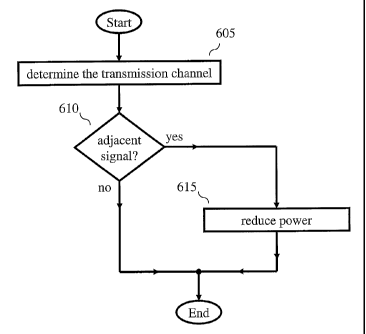
invention is
shown in FIG. 22. In step 605, CPE 250 determines a channel to use for
transmission. CPE
250 can either select a channel from the above-mentioned available channel
list, or negotiate
with BS 205 in order to determine which channel to use. Once a channel is
selected for
transmission, CPE 250 determines in step 610 if an incumbent signal is present
on an
adjacent channel (either above or below the currently selected transmission
channel). CPE
250 can determine if an incumbent signal is on an adjacent channel in any
number of ways.
For example, CPE 250 can simply check the available channel list. If the
adjacent channels
are indicated as available, then CPE 250 can presume that there are no
incumbent signals on
the adjacent channels. However, if any of the adjacent channels are not
indicated as
available, then CPE 250 assumes that an incumbent signal is present on an
adjacent channel.
Alternatively, CPE 250 can perform channel sensing on the adjacent channels.
[0047] If, in step 610, it is determined that an incumbent signal is on an
adjacent
channel, then CPE 250 reduces the power level of its transmitted signal in
step 615. For
example, if a D/U (Desired-to-Undesired) signal power ratio for a TV broadcast
is 20 dB
CA 02627439 2008-04-25
WO 2007/056081 PCT/US2006/042849
(decibels), then, upon detection of an adjacent TV broadcast, the WRAN
endpoint reduces its
transmission power by 20 dB. Turning briefly to FIG. 23, an illustrative
embodiment of an
OFDM modulator 650 for use in transceiver 285 is shown. In accordance with the
principles
of the invention, OFDM modulator 650 receives signal 649, which is
representative of a
5 data-bearing signal, and modulates this data-bearing signal, for broadcast
on the selected
transmission channel. The transmission power level of the resulting OFDM
signal 651 is
controlled via signal 648, e.g., from processor 295 of FIG. 4.
[0048] Also, it should be noted that FIG. 22 only indicates that portion of
transmission
power control related to the inventive concept. Simply because CPE 250 does
not detect an
10 adjacent incumbent signal does not necessarily mean that CPE 250 does not
perform other
forms of transmission power control. For example, a BS and a CPE can
dynamically adapt
the transmission power based on any criteria such as path loss, link margin
estimates,
channel measurement results, transmission power constraints, etc.
[0049] In addition, a BS may request a CPE to report transmission power and
link
15 margin information. This is illustrated in the message flow diagram of FIG.
24. BS 205
sends a TPC request 681 to CPE 250. The latter responds with TPC report 682.
Some
illustrative information elements for use in a TPC report are shown in FIG.
25. TPC report
682 comprises two information elements (IE): transmit power IE 687 and
estimated link
margin IE 686. Thus, the power level of the transmitted signal from CPE 250
and an
estimated link margin are sent to another wireless endpoint. Likewise, a CPE
may use a TPC
Request message to request a BS to report transmission power and link margin
information.
This is illustrated in the message flow diagrain of FIG. 26. CPE 250 sends a
TPC request
691 to BS 205. The latter responds with TPC report 692. In addition, a BS may
issue a
control message (not shown) to a CPE to change the maximum allowed
transmission power
of the CPE according to variations in the channel environment.
[0050] An illustrative frame 100 for use in communicating information between
BS 205
and CPE 250 (such as the above-described TPC request and TPC report) is shown
in FIG.
27. Other than the inventive concept, frame 100 is similar to an OFDMA frame
as described
in IEEE 802.16-2004, "IEEE Standard for Local and metropolitan area networks,
Part 16:
Air Interface for Fixed Broadband Wireless Access Systems". Frame 100 is
representative
of a time division duplex (TDD) system in which the same frequency band is
used for uplink
(UL) and downlink *(DL) transmission. As used herein, uplink refers to
communications
CA 02627439 2008-04-25
WO 2007/056081 PCT/US2006/042849
16
from CPE 250 to BS 205, while downlink refers to communications from BS 205 to
CPE
250. Each frame comprises two subfraines, a DL subframe 101 and a UL subframe
102. In
each frame, time intervals are included to enable BS 205 to turn around (i.e.,
switch from
transmit to receive and vice versa). These are shown in FIG. 27 as an RTG
(receive/transmit
transition gap) interval and a TTG (transmit/receive transition gap) interval.
Each subframe
conveys data in a number of bursts. Information about the frame and the number
of DL
bursts in the DL subframe and the number of UL bursts in the UL subframe are
conveyed in
frame control header (FCH) 77, DL MAP 78 and UL MAP 79. Each frame also
includes a
preamble 76, which provides frame synchronization and equalization.
[0051] As described above, the performance of a WRAN system is enhanced by
using a
transmit power control mechanism such that a wireless endpoint reduces its
transmission
power level upon detection of an incumbent signal on an adjacent channel. It
should be
noted that although the inventive concept was described in the context of CPE
250 of FIG. 4,
the invention is not so limited and also applies to, e.g., BS 205. Further,
although channel
sensing was described in the context of the technique illustrated in FIGs. 5
through 8, the
inventive concept is also not so limited. Other forms of channels sensing may
be used. For
example, an illustrative portion of a receiver 805 for use in CPE 250 is shown
(e.g., as a part
of transceiver 285) in FIG. 28. Only that portion of receiver 805 relevant to
the inventive
concept is shown. Receiver 805 comprises tuner 810, signal detector 815 and
controller 825.
The latter- is representative of one, or more, stored-program control
processors, e.g., a
microprocessor (such as processor 290), and these do not have to be dedicated
to the
inventive concept, e.g., controller 825 may also control other fitnctions of
receiver 805. In
addition, receiver 805 includes memory (such as memory 295), e.g., random-
access memory
(RAM), read-only memory (ROM), etc.; and may be a part of, or separate from,
controller
825. For simplicity, some elements are not shown in FIG. 28, such as an
automatic gain
control (AGC) element, an analog-to-digital converter (ADC) if the processing
is in the
digital domain, and additional filtering. Other than the inventive concept,
these eleinents
would be readily apparent to one skilled in the art. In this regard, the
embodiments described
herein may be implemented in the analog or digital domains. Further, those
skilled in the art
would recognize that some of the processing may involve complex signal paths
as necessary.
In the context of channel sensing, tuner 810 is tuned to different ones of the
channels by
controller 825 via bidirectional signal path 826 to select particular TV
channels. For each
CA 02627439 2008-04-25
WO 2007/056081 PCT/US2006/042849
17
selected channel, an input signal 804 may be present. Input signal 804 may
represent an
incumbent wideband signal such as a digital VSB modulated signal in accordance
with the
above-mentioned "ATSC Digital Television Standard", an NTSC TV signal or an
incumbent
narrowband signal. If there is an incumbent signal in the selected channel,
tuner 810
provides a downconverted signal 806 to signal detector 815, which processes
signal 806 to
determine if signal 806 is a wideband incumbent signal or a narrowband
incumbent signal.
Signal detector 815 provides the resulting information to controller 825 via
path 816. As
such, the inventive concept applies to searching for any signals, wideband
(e.g., NTSC) or
narrowband, that may exist on adjacent channels. In this regard, the transmit
power level
may be adjusted in step 615 of FIG. 22 by different amounts depending on the
type of
adjacent incumbent signal.
[0052] In view of the above, the foregoing merely illustrates the principles
of the
invention and it will thus be appreciated that those skilled in the art will
be able to devise
numerous alternative arrangements which, although not explicitly described
herein, embody
the principles of the invention and are within its spirit and scope. For
example, although
illustrated in the context of separate functional elements, these functional
elements may be
embodied in one, or more, integrated circuits (ICs). Similarly, although shown
as separate
elements, any or all of the elements may be implemented in a stored-program-
controlled
processor, e.g., a digital signal processor, which executes associated
software, e.g.,
corresponding to one, or more, of the steps shown in, e.g., FIG. 22, etc.
Further, the
principles of the invention are applicable to other types of communications
systems, e.g.,
satellite, Wireless-Fidelity (Wi-Fi), cellular, etc. Indeed, the inventive
concept is also
applicable to stationary or mobile receivers. It is therefore to be understood
that numerous
modifications may be made to the illustrative embodiments and that other
arrangements may
be devised without departing from the spirit and scope of the present
invention as defined by
the appended claims.