Language selection

Search

Patent 2627651 Summary

Third-party information liability

Some of the information on this Web page has been provided by external sources. The Government of Canada is not responsible for the accuracy, reliability or currency of the information supplied by external sources. Users wishing to rely upon this information should consult directly with the source of the information. Content provided by external sources is not subject to official languages, privacy and accessibility requirements.

Claims and Abstract availability

Any discrepancies in the text and image of the Claims and Abstract are due to differing posting times. Text of the Claims and Abstract are posted:

  • At the time the application is open to public inspection;
  • At the time of issue of the patent (grant).
(12) Patent Application: (11) CA 2627651
(54) English Title: OPTICAL SWITCHING DEVICE
(54) French Title: DISPOSITIF DE COMMUTATION OPTIQUE
Status: Dead
Bibliographic Data
(51) International Patent Classification (IPC):
  • G02F 1/19 (2019.01)
(72) Inventors :
  • DAM, BERNARD (Netherlands (Kingdom of the))
  • GRIESSEN, RONALD PIERRE (Netherlands (Kingdom of the))
  • LOHSTROH, WIEBKE (Germany)
  • PASTUREL, MATHIEU RAYMOND HENRI (Netherlands (Kingdom of the))
  • SLAMAN, MARINUS JOHANNES (Netherlands (Kingdom of the))
(73) Owners :
  • STICHTING ENERGIEONDERZOEK CENTRUM NEDERLAND (Netherlands (Kingdom of the))
(71) Applicants :
  • ADVANCED CHEMICAL TECHNOLOGIES FOR SUSTAINABILITY (Netherlands (Kingdom of the))
(74) Agent: RIDOUT & MAYBEE LLP
(74) Associate agent:
(45) Issued:
(86) PCT Filing Date: 2006-10-27
(87) Open to Public Inspection: 2007-05-03
Examination requested: 2011-10-07
Availability of licence: N/A
(25) Language of filing: English

Patent Cooperation Treaty (PCT): Yes
(86) PCT Filing Number: PCT/NL2006/050268
(87) International Publication Number: WO2007/049965
(85) National Entry: 2008-04-28

(30) Application Priority Data:
Application No. Country/Territory Date
1030299 Netherlands (Kingdom of the) 2005-10-28

Abstracts

English Abstract


A hydrogen permeable optical reflective layer (4) of a transition metal is
deposited on transition metal (hydride) layer (3) which can switch from a
black absorbing state. A hydrogen permeable catalytic layer (5) of a
transition metal is deposited on top of the reflective layer (4). Ti and/or Pd
may be used as transition metal(s) in all of the three layers (3,4,5). Co-
sputtering may be used to deposit a transition metal (hydride) switching layer
(3) with a maximum thickness of 100 nm on a substrate (2) which can be of any
material. The thickness of the optical reflective layer (4), which is larger
than the thickness of the switching layer (3), is more than 10 nm (but
preferably 50-200 nm) so that there is (no or) little transmission. The
thickness of the catalytic layer (5) is about 10 nm. If a detector (11) is
included one can produce a hydrogen sensor. Alternatively, one can produce a
temperature controlled solar energy converter (17) by including a fluid heater
(18).


French Abstract

La présente invention concerne une couche réfléchissante optique perméable à l~hydrogène (4) d~un métal de transition, qui est déposée sur une couche (hybride) de métal de transition (3) pouvant commuter d~un état absorbant le noir. Une couche catalytique perméable à l~hydrogène (5) d~un métal de transition est déposée sur la couche réfléchissante (4). Il est possible d~utiliser du Ti et/ou de Pd en tant que métal ou métaux de transition dans chacune des trois couches (3, 4, 5). Il est possible d~utiliser la co-pulvérisation pour déposer une couche de commutation (hybride) de métal de transition (3) avec une épaisseur maximale de 100 nm sur un substrat (2) d~un matériau quelconque. L~épaisseur de la couche réfléchissante optique (4), supérieure à l~épaisseur de la couche de commutation (3), est supérieure à 10 nm (mais de préférence comprise entre 50 et 200 nm) de telle sorte que la transmission est faible (voire nulle). L~épaisseur de la couche catalytique (5) est d~environ 10 nm. En incluant un détecteur (11), il est possible de produire un détecteur d~hydrogène. Alternativement, il est possible de produire un convertisseur d~énergie solaire à régulation de température (17) en incluant un réchauffeur de fluide (18).

Claims

Note: Claims are shown in the official language in which they were submitted.


6
Claims

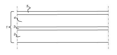
1. Optical switching device (1) comprising a substrate (2), an active metal
layer
(3) provided on said substrate having different optical properties at
loading/unloading
with/of hydrogen and a catalytic layer (5), characterized in that, between
said active
metal layer and said catalytic layer an auxiliary layer (4) comprising a
transition metal
layer is provided having a thickness larger than the thickness of said active
metal layer
and being hydrogen permeable.

2. Optical switching device according to claim 1, wherein said auxiliary metal

layer is a transition metal based layer.

3. Optical switching device according to claim 1, wherein said active metal
layer
is a rare-earth based layer.

4. Optical switching device according to one of the preceding claims, wherein
said active metal layer is a Mg based layer.

5. Optical switching device according to one of the preceding claims
comprising
a black switching condition.

6. Optical switching device according to one of the preceding claims, wherein
said active metal layer has a thickness of 100 nm at maximum.

7. Optical switching device according to one of the preceding claims, wherein
said substrate comprises glass.

8. Optical switching device according to one of the preceding claims, wherein
the
metal of said catalytic metal layer comprises titanium and/or palladium and/or
silver.

9. Optical switching device according to one of the preceding claims, wherein
said transition metal layer has a thickness of 10 nm - 2 µm.


7
10. Optical switching device according to one of the preceding claims, wherein
the transition metal of the active transition metal layer comprises nickel,
titanium,
palladium.

11. Method for preparing an optical switching device comprising the provision
of
a substrate and the subsequent deposition of an active metal layer having a
thickness
smaller than 100 nm, an auxiliary layer comprising a transition metal layer
and having
a thickness larger than 10 nm and a catalyst layer.

12. Method according to claim 11, wherein at least one of said deposition
steps
comprises (co) sputtering.

13. Mirror comprising an optical switching device with a substrate (2), an
active
metal layer (3) provided on said substrate having different optical properties
at
loading/unloading with/of hydrogen and a catalytic layer (5), characterized in
that,
between said active metal layer and said catalytic layer an auxiliary layer
(4)
comprising a transition metal layer is provided having a thickness larger than
the
thickness of said active metal layer and being hydrogen permeable.

14. Hydrogen sensor comprising an optical switching device with a substrate
(2),
an active metal layer (3) provided on said substrate having different optical
properties
at loading/unloading with/of hydrogen and a catalytic layer (5), characterized
in that,
between said active metal layer and said catalytic layer an auxiliary layer
(4)
comprising a transition metal layer is provided having a thickness larger than
the
thickness of said active metal layer and being hydrogen permeable.

15. Hydrogen sensor according to claim 13 or 14, comprising an optical sensor
(11) to monitor the state of said optical switching device.

16. Hydrogen sensor according to claim 15, wherein a fibre optic (7, 9) is
coupled
between said optical switching device (6) and said optical sensor (11).


8
17. Energy conversion assembly comprising a fluid heater (13) and in the
direction of incident light (16) in front of said fluid heater an optical
switching device
(14) with a substrate (2), an active metal layer (3) provided on said
substrate having
different optical properties at loading/unloading with/of hydrogen and a
catalytic layer
(5), characterized in that, between said active metal layer and said catalytic
layer an
auxiliary layer (4) comprising a transition metal layer is provided having a
thickness
larger than the thickness of said active metal layer and being hydrogen
permeable.

18. Energy conversion assembly according to claim 17 comprising a photovoltaic
element (13) wherein in the position of use in the direction of incident light
(16) the
fluid heater (13) is behind said photovoltaic element, wherein said switching
device
(14) is arranged between said photovoltaic element and said fluid heater.

Description

Note: Descriptions are shown in the official language in which they were submitted.


CA 02627651 2008-04-28
WO 2007/049965 PCT/NL2006/050268
1
Optical switching device.

The present invention relates to an optical switching device comprising a
substrate, an active metal layer provided on said substrate having different
optical
properties at loading/unloading with/of hydrogen and a catalytic layer. Such a
device is
generally known in the art. As active metal a magnesium transition metal alloy
is for
example used. It has been found that a magnesium nickel layer being provided
on a
substrate and on top of which a catalyst such as palladium is provided will
turn into a
magnesium nickel hydride layer near the substrate when hydrogen is added to
such
layer. This means that although hydrogen enters the device through the
catalyst the
hydride phase nucleates first at the magnesium nickel layer/substrate
interface. This
leads to a self-organized layering of the sample. With increasing hydrogen
absorption
the hydride layer grows until the whole magnesium nickel layer is converted to
a
hydride. Such layers are also known as VAriable REflection Metal hydrides
(VAREM)
or metal-hydride switchable mirrors.
Depending on the conversion such a layer can have properties ranging from
reflective through black to transparent. The transparent and reflective modes
are
relatively stable and easy to obtain and maintain. However a stable black
situation in
which the light entering through the substrate is absorbed, is difficult to
maintain. It
depends sensitively on external parameters such as temperature and H2 gas
pressure.
The different physical appearances are preferably obtained by loading with
hydrogen or unloading hydrogen for example by using oxygen. Electrochemical
hydrogenation/dehydrogenation can also be used. The hydrogen concentration in
which
the black condition is obtained is very critical.
US 2002/101413 discloses a light switching device wherein a switching film is
provided with a catalyst Pd-layer on which a hydrogen ion conducting
electrolyte layer
is provided. On this hydrogen ion conducting electrolyte layer a hydrogen
storage layer
is present. With this device one actively controls the amount of hydrogen and
thereby
the optical state of the active layer.
The invention aims to provide an optical switching device in which the black
condition is both easily obtained and on the other hand can easily be
maintained.
According to the invention this is realized in that, between said active metal
layer
and said catalytic layer an auxiliary layer comprising a transition metal
layer is


CA 02627651 2008-04-28
WO 2007/049965 PCT/NL2006/050268
2
provided having a thickness larger than the thickness of said active metal
layer and
being hydrogen permeable.
According to the invention there is no longer a "self-organized" double layer
needed to provide for the large change in optical behavior. The self organized
double
layer is according to the invention replaced by an auxiliary layer which has
been
separately provided and comprises a transition metal layer. In contrast to the
prior art
an auxiliary layer is provided between the metal layer and the catalytic
layer.
It has been found that by using an artificially provided auxiliary layer a
stable
black condition is obtained of the magnesium transition metal (hydride) layer.
It has
also been found that after unloading the hydrogen and reloading with hydrogen
reproducible results are obtained which means that switching can be obtained
in a
reproducible way making the optical switching device suitable for all kinds of
applications.
Furthermore it has been found that a better contrast can be obtained and
oxidation
protection is further improved.
The thickness of the transition metal layer should be such that there is no or
little
transmission.
The active metal layer can comprise any metal which has changing optical
properties at loading or unloading with hydrogen. As example magnesium or
magnesium based transition metals are mentioned. Also combination of several
elemental metals can be used or metal hydrides such as yttrium hydride being
in the
metallic phase. Further possibilities for the active layer can be rare earths
including
yttrium, possibly in combination with a transition metal, magnesium and so on.
Another preferred option is the use of Mg2Ni as active layer.
According to a preferred embodiment of the invention the active layer has a
thickness of 100 nm at maximum. The transition metal layer or auxiliary layer
has a
thickness starting from 10 nm and is preferably not more than 1 m.
The auxiliary layer can comprise layers being positioned on top of each other
and
comprising a different transition metal for example titanium, nickel and/or
niobium. It
is also possible that different layers are stacked on each other having a
different
structure, as long as the layer stack allows for hydrogen diffusion and is
optically
reflective.
The substrate according to the invention can comprise any material such as
glass.


CA 02627651 2008-04-28
WO 2007/049965 PCT/NL2006/050268
3
The transition metal of the transition metal layer can comprise any transition
metal known from the periodic system and in more particular titanium and/or
palladium.
The same applies to the transition metal in the magnesium transition metal
active
layer which preferably comprises nickel.
According to an advantageous embodiment the optical switching device is
passive. This means that switching is only obtained by gas pressure and not to
the use
of electrical tension. However, an embodiment being electrolytically switched
is within
the range of the subject application.
The optical switching device according to the invention can be prepared by
deposition of the several layers mentioned above on a substrate. This
deposition can
comprise sputtering such as co-sputtering of the several metals to obtain for
example
the magnesium transition metal layer.
As indicated above there are many applications for the optical switching
device
according to the invention. The most simple one is the use as a mirror which
can switch
from the black absorbing phase to the reflective phase.
Because optical switching is obtained depending on the presence of hydrogen
according to a further embodiment of the invention it is possible to provide a
hydrogen
sensor having an optical switch as described above. Through a sensor the
optical
properties of an optical switching device according to the invention can be
monitored.
It is possible that there is a distance between the optical switching device
and the
optical sensor which can be bridged by fibre optics. Furthermore it is
possible to
monitor a large number of optical switching devices with a single optical
sensor.
The optical switching device can be embodied to have the optical properties
reversible or non-reversible. An example for the last possibility is the use
of a tag
which shows exposure of an article or person in an environment in which
hydrogen
might be present. Such a tag can be disposable.
The invention can also be used in an energy conversion assembly comprising a
photovoltaic element and a water heater. Such an assembly can for example be
arranged on a roof wherein the incident light first hits the photovoltaic
element. Under
some conditions it might be desirable that radiation is not transferred to the
water
heater whilst in other conditions it is desirable to heat the water. These
different


CA 02627651 2008-04-28
WO 2007/049965 PCT/NL2006/050268
4
conditions can be switched by placing an optical switching device according to
the
invention between such photovoltaic element and a water heater.
The invention will be further elucidated referring to embodiments shown in the
drawing wherein:
Fig. 1 schematically shows the layer structure of an optical switching device
according to the invention;
Fig. 2 schematically shows the application of the optical switching device as
a
hydrogen sensor; and
Fig. 3 shows the use in an energy conversion assembly.
In fig. 1 an example for an optical switching device according to the
invention is
generally referred to by 1. A substrate 2 is present which can be any
material. However,
preferably glass is used as is usual in optical devices. On top of the glass a
30 nm
magnesium transition metal layer as active layer is provided such as an Mg2Ni
layer.
On top of this active layer 3 an auxiliary layer 4 according to the invention
is arranged.
This is a transition metal layer such as a titanium layer or a palladium
layer. The
thickness thereof is from 10 nm and more preferably between 50 and 200 nm. On
top of
the auxiliary layer a catalyst layer 5 is provided being for example a
palladium layer
having a thickness of about 10 nm.
If hydrogen is added to such an optical switching device 1 the Mg2Ni layer
will
convert to Mg2NiH4. The optical properties of this material are completely
different
from Mg2Ni.
According to the invention an artificial double layer comprising the layers 3
and
4 has been synthesized. Mg2NiH4 is transparent while hydrogenated titanium
which is
for example used in layer 4 remains reflective.
During tests it revealed that the reflection observed through the layer
structure in
an energy range 1.25 - 3 eV goes from around 60% before hydrogenation to about
5%
at 1.9 - 2 eV in the totally hydrogenated layer 3. This is a ratio of 12 in
reflection. At
room temperature such hydrogenation, when a 5% H2 in Ar is used is effected in
typical 10 seconds depending on the thickness of layer 4. A sensitivity of
0.3% H2 has
been observed.
In fig. 2 the use of the optical switching device according to the invention
in a
hydrogen sensor is shown. The optical switching device according to the
invention is
indicated with 6 which is connected through fibre optic 7, 9 (with the use of
a


CA 02627651 2008-04-28
WO 2007/049965 PCT/NL2006/050268
bifurcator 8) to a detector 11. 10 is a light source (for example a lamp or a
laser) to
provide light to the switchable mirror 6. If only small quantities of hydrogen
are present
in the room in which the optical switching device is present immediately a
remarkable
change in reflective properties of the optical switching device occurs which
is easily
5 detected by detector 11. Detector 11 can be connected to a number of fibre
optics being
connected to optical switching devices in the same room or in different areas.
In fig. 3 a further application of the invention is shown. On a schematically
shown roof 15 an energy conversion assembly 17 is provided. This comprises a
photovoltaic element 13, an optical switch 14 according to the invention and a
fluid
heater 18 such as a water heater having heating tubes 19. Depending on the
conditions
it is desirable that incident light as indicated by arrow 16 will or will not
reach heater
18. By controlling optical switching device 14 as indicated above this can be
prevented.
If the optical switching is in the black condition heat will be absorbed and
transferred to
heater 18. If it is in the reflective mode the heat will not be absorbed and
reflected back
through to the photovoltaic element 13. Even without the photovoltaic device,
the
invention can be used solely to control the temperature of the water heater.
In the above some applications of the photovoltaic switching device according
to
the invention have been discussed. However it should be understood that
further
applications are possible both on Earth and in space. As example the use on
the outer
surface of a satellite is mentioned.

Representative Drawing
A single figure which represents the drawing illustrating the invention.
Administrative Status

For a clearer understanding of the status of the application/patent presented on this page, the site Disclaimer , as well as the definitions for Patent , Administrative Status , Maintenance Fee  and Payment History  should be consulted.

Administrative Status

Title Date
Forecasted Issue Date Unavailable
(86) PCT Filing Date 2006-10-27
(87) PCT Publication Date 2007-05-03
(85) National Entry 2008-04-28
Examination Requested 2011-10-07
Dead Application 2013-10-29

Abandonment History

Abandonment Date Reason Reinstatement Date
2012-10-29 FAILURE TO PAY APPLICATION MAINTENANCE FEE

Payment History

Fee Type Anniversary Year Due Date Amount Paid Paid Date
Application Fee $400.00 2008-04-28
Maintenance Fee - Application - New Act 2 2008-10-27 $100.00 2008-04-28
Registration of a document - section 124 $100.00 2008-09-03
Maintenance Fee - Application - New Act 3 2009-10-27 $100.00 2009-07-09
Registration of a document - section 124 $100.00 2010-09-02
Maintenance Fee - Application - New Act 4 2010-10-27 $100.00 2010-09-29
Maintenance Fee - Application - New Act 5 2011-10-27 $200.00 2011-08-22
Request for Examination $800.00 2011-10-07
Owners on Record

Note: Records showing the ownership history in alphabetical order.

Current Owners on Record
STICHTING ENERGIEONDERZOEK CENTRUM NEDERLAND
Past Owners on Record
ADVANCED CHEMICAL TECHNOLOGIES FOR SUSTAINABILITY
DAM, BERNARD
GRIESSEN, RONALD PIERRE
LOHSTROH, WIEBKE
PASTUREL, MATHIEU RAYMOND HENRI
SLAMAN, MARINUS JOHANNES
Past Owners that do not appear in the "Owners on Record" listing will appear in other documentation within the application.
Documents

To view selected files, please enter reCAPTCHA code :


To view images, click a link in the Document Description column. To download the documents, select one or more checkboxes in the first column and then click the "Download Selected in PDF format (Zip Archive)" or the "Download Selected as Single PDF" button.

List of published and non-published patent-specific documents on the CPD .

If you have any difficulty accessing content, you can call the Client Service Centre at 1-866-997-1936 or send them an e-mail at CIPO Client Service Centre.


Document
Description 
Date
(yyyy-mm-dd) 
Number of pages   Size of Image (KB) 
Cover Page 2008-08-08 1 40
Description 2008-04-28 5 260
Representative Drawing 2008-04-28 1 1
Claims 2008-04-28 3 103
Abstract 2008-04-28 2 73
Drawings 2008-04-28 2 24
Assignment 2008-04-28 6 156
PCT 2008-04-28 3 92
PCT 2008-04-28 1 44
Assignment 2008-09-03 4 174
Correspondence 2008-11-12 1 2
Fees 2009-07-09 1 37
Assignment 2010-09-02 2 66
Fees 2010-09-29 1 35
Prosecution-Amendment 2011-10-07 1 35