Note: Descriptions are shown in the official language in which they were submitted.
CA 02627756 2008-04-29
WO 2007/060128 PCT/EP2006/068548
"A LED driving arrangement"
***
Field of the invention
The present invention relates to driving arrangements
for light emitting diodes (LEDs).
The invention was developed with specific attention paid
to its possible use in driving LEDs used as lighting sources
(so-called high-flux LEDs), where a good power factor is a
basic requirement to be complied with.
Description of the related art
A good candidate circuit arrangement for driving LEDs is
the so-called half-bridge (HB) resonant topology. In such an
arrangement, one or more LEDs are driven via the secondary
winding of a transformer. The primary winding of the
transformer is part of a resonant circuit and is fed via a
half-bridge arrangement driven in by a half-bridge
controller. The voltage fed to the resonant circuit is thus
essentially a square wave having a frequency in the range of
20=200 kHz whose envelope is modulated by the 50-60 Hz sine
waveform of the mains voltage.
A basic drawback of such an arrangement lies in that
energy transfer cannot take place when the input voltage to
the half-bridge is lower than the LED threshold voltage
multiplied by the transformer turn ratio (primary
turns/secondary turns). This leads to rather long zero
current periods on the mains and, consequently, to a bad
power factor.
CA 02627756 2008-04-29
WO 2007/060128 2 PCT/EP2006/068548
This problem could be notionally solved by decreasing
the transformer turn ratio (primary turns/secondary turns).
However, this would lead to an undesirable adaptation
mismatch with the LED or LEDs being driven and a similarly
undesired strong current increase on the primary side.
In this latter respect, it is worth mentioning that the
LED driving arrangements being considered are generally
expected to be included in compact, expectedly cheap, low-
power drivers that must also comply with rather strict
regulations in terms of safety and electromagnetic
interference (EMI ) .
Object and summary of the invention
The object of the present invention is thus to provide
an effective solution to the problems described in the
foregoing in connection with the half-bridge topology.
According to the present invention, that object is
achieved by means of the arrangement having the features set
forth in the claims that follow. The claims are an integral
part of the disclosure of the invention provided herein.
Brief description of the annexed representations
The invention will now be described, by way of example
only, by referring to the enclosed representations, wherein:
- figure 1 is a block diagram of first embodiment of the
arrangement described herein,
- figure 2 is a block diagram illustrating an
alternative embodiment of the arrangement described herein,
and
- figures 3 and 4 are diagrams representative of
operation of the circuits of figures 1 and 2.
Detailed description of preferred embodiments of the
invention
CA 02627756 2008-04-29
WO 2007/060128 3 PCT/EP2006/068548
As a first step, a general description will be provided
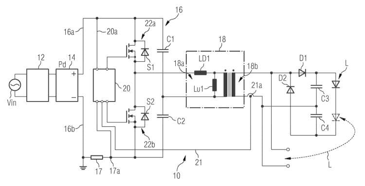
of the circuit arrangements illustrated in figures 1 and 2.
Both figures show a circuit arrangement (generally
indicated as 10) for use as drive circuit for one or more
LEDs L. In both figures only one LED L is shown with the
proviso that the arrangement described can be used for
driving one or more additional LEDs, connected in series in
each rectifier and/or connecting the rectifiers in parallel,
as schematically indicated in both figures.
In a manner known per se, the or each series of LED L is
driven via a "voltage doubler" arrangement including a pair
of diodes Dl, D2 and a pair of capacitors C3, C4. These
diodes act as rectifiers in order to ensure that the LED o
LEDs in question are traversed by electrical current in the
direction where the LED acts as a light source.
Alternatively, the or each series of LED L could be driven
via a full bridge rectifier.
The circuit 10 is connected in use to an ac mains source
Vin (typically a 200=240V or 100=120 50-60Hz mains source).
The overall arrangement of the device 10 includes,
starting from the mains source Vin and proceeding
"downstream" towards the LED or LEDs L:
- a line filter 12 to filter out undesired high-frequency
noise components from the power feed,
- a bridge rectifier 14 that feeds a half-bridge
rectifier 16, and
- a transformer 18 having a primary winding 18a fed by
the half-bridge and a secondary winding 18b that in turn
feeds the LED or LEDs L.
The bridge rectifier 14 supplies the half-bridge
arrangement 16 essentially as voltage signals over a first
line 16a referred to a second line 16b. A resistor 17 is
CA 02627756 2008-04-29
WO 2007/060128 4 PCT/EP2006/068548
arranged over the second line 16b between ground and a point
17a. At the point 17a a voltage develops and can be sensed as
a measure of the intensity of the current fed to the half-
bridge 16.
The "current intensity" signal at point 17a is fed to a
controller circuit 20. The control circuit or controller 20
equally senses (via a line 20a) the mains voltage signal over
the line 16a as well a LED current feedback signal. This LED
current feedback signal is provided over a line 21 as better
detailed in the following.
The controller 20 controls two electronic switches 22a,
22b, typically in the form of MOSFETs S1, S2.
Unless otherwise specified in the following, the general
circuit layout described so far corresponds to a general
arrangement known in the art, thus making it unnecessary to
provide herein a more detailed description of the structure
and operation thereof. This applies a i.e. to the capability,
for the controller 20, to selectively adapt to different
operating conditions the drive signal applied to the
electronic switches 22a, 22b.
This is achieved primarily by varying the frequency of
the square wave driving signal applied to the control gates
of the electronic switches 22a, 22b as a function of the
signals sensed at 17a and via the lines 20a and 22 in order
to stabilise the operating conditions of the LED or LEDs L.
The electronic switches 22a, 22b driven by the
controller 20 are arranged over two arms of the half-bridge
arrangement 16 connecting the two lines 16a and 16b to one of
the ports or terminals of the primary winding 18a of the
transformer 18.
Two capacitors Cl, C2 are similarly arranged on the two
other arms of the half-bridge arrangement 16, namely the two
arms connecting the lines 16a, 16b with the other port of
terminal of the primary winding 18a of the transformer 18.
In the arrangement illustrated in figure 1, the
capacitors Cl and C2 form a parallel resonant circuit
together with the magnetising inductance Lul of the
CA 02627756 2008-04-29
WO 2007/060128 5 PCT/EP2006/068548
transformer 18. The magnetising inductance Lul of the
transformer can be modelled as an inductor connected in
parallel with the primary winding 18a of the transformer 18.
The resonant circuit in question include also an
inductor LD1 series-connected with the primary winding 18a,
representing the leakage inductance of the transformer.
Whatever the specific arrangement adopted, typical
values of the resonance frequency in question lie below the
switching frequency.
The basic principle underlying operation of the
arrangement illustrated in figure 1 provides for the resonant
circuit in question to boost the voltage across the LED or
LEDs around the zero-crossing instants of the voltage from
the mains. Such a voltage boosting effect ensures that energy
transfer takes place even when the input voltage of the half-
bridge arrangement 16 is lower than the LED threshold voltage
(multiplied by the turn ratio of the transformer 18).
Specifically, the parallel resonant converter, including
the resonant inductance (Lul plus LD1), has the capability of
boosting up the voltage up to the LED threshold voltage. Such
a boosting effect of the converter increases as the switching
frequency applied by the controller 20 to the electronic
switches 22a, 22b approaches the resonance frequency of the
resonant arrangement.
This principle of operation is better explained by
referring to the diagram of figure 3.
Essentially, the diagram in question portraits the
behaviour of the input voltage-to-LED voltage gain G
(ordinate scale) against the switching frequency f of the
controller 20 (abscissa scale).
The peaked behaviour of the diagram is related :.o the
quality factor Q of the resonant circuit, which can be
designed (in known manner) in order to match the specific
operation requirements of the circuit.
CA 02627756 2008-04-29
WO 2007/060128 6 PCT/EP2006/068548
In general terms, if the controller switching frequency
changes from a "nominal" value fl to another value f2 which
is closer to the resonance frequency fr of the resonant
circuit (i.e. the peak of the diagram of figure 3), the gain
value G is correspondingly increased from a first value G1 to
a second, higher value G2.
Typical values for fl are some tens of kHz over f2, while
typical values for f2 are some tens of kHz over fr.
Consequently, the controller 20 can be operated (in a
manner known per se) in order to change the frequency of
drive signal applied to the electronic switches 22a, 22b
during the semi-period of the alternated sine-wave input line
voltage. This is done decreasing that frequency (e.g. from fl
to f2) around the zero-crossing points of the input voltage
to render the frequency in question closer to the resonant
frequency fr in order to boost the input voltage, while the
frequency of drive signal applied to the electronic switches
22a, 22b is increased (e.g. by restoring it to fl) over the
rest and around the peak of the mains voltage.
Such behaviour is schematically represented in the
diagram of figure 4.
There, the switching signal SW applied by the controller
20 to the gates of the electronics switches 22a, 22b is
portrayed on a common time scale t against a semi-period of
the input voltage IW derived from the mains source Vin.
The specific law ruling the variation of the frequency
of the switching signal SW over the semi-period of the input
voltage IW may be adapted at will (possibly as a result of
experimental tests or automatically by means of a multiplier)
as a function of the resonance diagram shown in figure 3 and
in accordance with the boosting effect desired.
The boosting mechanism previously described in
connection with figure 3, provides for the switching
frequency of the converter 20 being rendered closer to the
CA 02627756 2008-04-29
WO 2007/060128 7 PCT/EP2006/068548
resonance frequency fr of the resonant arrangement including
to the capacitor Cl, C2 by making such a switching frequency
lower (i.e. by passing from the frequency fl to the frequency
f2). Those of skill in the art will promptly appreciate that
a similar effect can - at least notionally - be implemented
in a complementary way, namely by selectively increasing the
switching frequency of the converter 20 when the boosting
effect is required. By referring to the graph of figure 3
this alternative arrangement would require the frequency fl
to be lower than the frequency f2, and the frequency f2 to be
in turn lower than the frequency fr.
While feasible, such an alternative arrangement
represents at present a less-preferred solution for a number
of reasons. These include i.e. the fact that the current
operating frequency fl of the controller 20 is generally
selected as a relatively high frequency. Additionally,
selecting a switching frequency below the resonance frequency
could imply an undesired increase of power losses on the
primary and secondary side.
The behaviour represented in figure 4 essentially
represents a sort of frequency modulation of the switching
frequency of the controller 20, which can be achieved by
known means by using the input voltage signal IV as the
modulating entity.
This mode of operation is fully compatible with
operating the controller 20 as a conventional PFC (Power
Factor Correction) controller including an inner mains
current feedback loop to force a sinusoidal mains current
shape and an outer loop to control the average LED current.
For that reason the controller 20 is made sensitive to the
input current (via the sensing resistor 17), the mains
voltage (via the line 20a) and the transformer current
measurement (via the line 21).
In the arrangement illustrated in figure 1, the LED
current cannot be measured on the primary side of the
CA 02627756 2008-04-29
WO 2007/060128 8 PCT/EP2006/068548
transformer 18 because the respective current is the sum of
the LED current and the resonance current.
For that reason the current intensity measurement
feedback line 21 is connected at 21a on the secondary side
of the transformer 18 (secondary winding 18b).
In the case of fixed output load, the outer controller
loop can be removed and a simple mains voltage feedforward
scheme can be added to ensure constant power feed to the LED
or LEDs at different line voltages.
The arrangement illustrated in figure 1 exhibits a number
of advantages.
It may take the form of a cheap circuit adapted to ensure
a good current matching between the LED or LEDs with
different values for the forward voltage Vf, by means of the
capacitor of the voltage-doubler C3 and C4, without sensing a
current feedback from each series of LEDs. Additionally, it
can be easily implemented to fulfil standards related to
harmonic generation such as the EN standard 61000-3-2 class
C. Additionally, the "wobbling" mechanism of the switching
frequency of the controller 20 described in connection with
figure 4 leads to a useful spread of the electromagnetic
noise generated: this spectrum spread is advantageous in
terms of reducing electromagnetic interference (EMI).
Moreover, the rectifier is typically placed outside with
respect to the housing of the power-supply unit, i.e. on the
LED module, in order to reduce the overall dimensions of the
power-supply unit itself.
All of the foregoing applies also to the alternative
embodiment illustrated in figure 2. In this alternative
embodiment an extra resonant inductor L2 is arranged in
CA 02627756 2008-04-29
WO 2007/060128 9 PCT/EP2006/068548
parallel with the primary winding of the transformer 18. In
figure 2 the magnetising inductance of the transformer 18 is
not explicitly shown as the current flowing through it can be
regarded as generally negligible in comparison with the
overall primary current.
Referring to figure 2, typical values for the
magnetising inductance Lul of the transformer 10 are in the
range of 1= 20 mH. Typical values for the leakage inductance
LD1 of the transformer 10 are in the range of 0.02 - 1 mH
while a suitable choice for L2 is in the range of 0.2 = 5 mH.
In the embodiment illustrated in figure 2, the LED
current feedback point 21a for the line 21 is arranged on the
primary side of the transformer 18. The signal provided on
the feedback line 21 is thus a correct measurement of the
load current and can be properly used to implement current
feedback/protections. Additionally, in the alternative
embodiment of figure 2, the resonant current is primarily
carried by the inductor L2 and total RMS current on the
primary windings of the transformer is correspondingly
reduced.
An additional inductor L4 (with a typical value in the
range of 0.02 = 2 mH) can be further arranged in series with
the parallel connection of the inductor L2 and the primary
winding 18a of the transformer to possibly further reduce the
resonance frequency fr of the converter.
Those of skill in the art will promptly appreciate that
both embodiments illustrated in figures 1 and 2 may further
include additional components.
For instance a capacitor can be arranged immediately
downstream of the diode bridge, in possible cooperation with
standard DM and/or CM filter, in order to filter out the
switching current of the half-bridge. Similarly, an
CA 02627756 2008-04-29
WO 2007/060128 10 PCT/EP2006/068548
additional inductor can be added in series to each cell in
order to improve current matching between parallel cells.
Without prejudice to the underlying principle of the
invention, the details and embodiments may vary, even
significantly, with respect to what has been described and
illustrated in the foregoing, by way of example only, without
departing from the scope of the invention as defined by the
annexed claims.