Note: Descriptions are shown in the official language in which they were submitted.
CA 02628465 2008-05-02
PCT/EP2006/067786 - 1 -
2005P13288WOUS
Description
Drive circuit for a switchable heating transformer of an
electronic ballast and corresponding method
Technical Field
The present invention relates to a drive circuit for a
switchable heating transformer of an electronic ballast with a
circuit input terminal for picking up an oscillating inverter
voltage (DC/AC converter), which has a variable inverter
frequency, and a switching device, to whose output terminal the
heating transformer can be connected. Furthermore, the present
invention relates to a corresponding method for switching a
heating transformer.
Prior Art
Depending on the application area, various preheating concepts
for ballasts for gas discharge lamps are conventional. These
include, for example, preheating via the resonant capacitor of
the load circuit, via an auxiliary winding on the lamp
inductor, via a resonant heating transformer and via a
switchable heating transformer. The most cost-intensive but
also most efficient solution for the preheating consists in a
switchable heating transformer.
A corresponding drive signal and a driver or level converter,
which are generally provided by an ASIC, are required for
driving a switchable heating transformer. This ASIC
conventionally also implements the entire sequence control.
However, there
CA 02628465 2008-05-02
PCT/EP2006/067786 - 2 -
2005P13288WOUS
are also less expensive ASICs on the market which do not
provide a drive signal for a heating transformer.
In principle, it has been possible to drive the swit:chable
heating transformer by a delay element instead of by the ASIC.
With this delay element, for example a PTC thermistor, a signal
can be produced which is only active for a short time directly
after the device has been switched on. This method of clriving
using a delay element does not allow for any synchroni.zation
with remotely controlled sequence control, however.
Description of the Invention
The object of the present invention therefore consists in
providing a simple drive circuit for a switchable heating
transformer, where synchronization wi_th remotely controlled
sequence control should be possible. A corresponding method
should also be made available.
According to the invention, this object is achieved by a drive
circuit for a switchable heating transformer of an electronic
ballast with a circuit input terminal for picking up an
oscillating inverter voltage, which has a variable inverter
frequency, and a switching device, to whose output terminal the
heating transformer can be connected, as well as a frequency
evaluation device, which is connected downstream of the circuit
input terminal and with which the inverter frequency can be
converted into a drive signal for the switching device.
CA 02628465 2008-05-02
PCT/EP2006/067786 - 3 -
2005P13288WOUS
Furthermore, the invention provides a method for switching a
heating transformer of an electronic ballast, by pickup of an
oscillating inverter voltage, which has a variable inverter
frequency, conversion of the inverter frequency into a drive
signal, and switching of the heating transformer (HT) as a
function of the drive signal.
The invention is based on the concept that, prior to starting
of the gas discharge lamp, the frequency in the load circuit is
higher than the nominal operating mode, in which the lamp is
lit and therefore the difference in frequency can be used to
drive the heating transformer prior to starting of the lamp.
If, therefore, the oscillating inverter voltage, which is
produced, for example, by the mid-point potential of a
half-bridge or full-bridge, is used for producing a drive
signal for the heating transformer, synchronizatiori with
remotely controlled sequence control of the ballast is
possible.
Preferably, the frequency evaluation device has a charge pump.
This makes it possible, using simple means, to convert the
frequency into a drive signal.
A voltage divider can be connected downstream of the charge
pump. As a result, the current produced by a charge pump can be
converted into a desired voltage. Favorably, this swi_tching
device comprises a MOSFET transistor. This component is
distinguished as a reliable swi_tching unit.
If the drive circuit according to the invention is installed in
an electronic ballast, a half-bridge,
CA 02628465 2008-05-02
PCT/EP2006/067786 - 4 -
2005P13288WOUS
for example, produces the oscillating inverter voltage. It is
advantageous here if the amplitude of the oscillating inverter
voltage is kept invariable since in this case the output signal
of the charge pump is directly proportional to the frequency of
the oscillating inverter voltage.
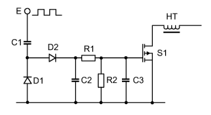
Brief Description of the Drawing
The present invention will now be explained in more detail with
reference to the attached drawing, which reproduces a circuit
diagram of a drive circuit according to the invention.
Preferred Embodiment of the Invention
The exemplary embodiment outlined in more detail below
represents a preferred embodiment of the present invention.
The figure illustrates a drive circuit for a heating
transformer HT. A square-wave oscillating inverter voltage,
which originates from a half-bridge mid-point (not
illustrated), is present at the input E of the circuit. A
charge pump is fed via the input E. Said charge pump contprises
the two capacitors Cl and C2 and the two diodes D1 and D2. The
capacitor Cl is connected at one terminal to the input E and at
the other terminal to the cathode of the diode Dl. The anode of
the diode Dl is connected to ground. The cathode of the diode
D1 is also connected to the anode of the diode D2. Finally, the
capacitor C2 is connected on one side to the cathode of the
diode D2 and on the other side to ground.
CA 02628465 2008-05-02
PCT/EP2006/067786 - 5 -
2005P13288WOUS
In the event of a positive input voltage, the capacitors Cl and
C2 are charged via the diode D2. In this case, the magnitude of
Cl determines the amount of charge supplied to C2. Given an
input voltage of zero, the diode D2 turns off and the capacitor
Cl is discharged via the diode Dl. This operation is repeated
with each period of an oscillating inverter or input voltage.
The mean current transferred by the charge pump is di_rectly
proportional to the frequency of the inverter (riot illustrated)
since, as the frequency increases, the charging operation to
the capacitor C2 takes place more and more often, with the
result that its voltage increases.
The voltage present at the capacitor C2 is adjusted in a
suitable manner via a resistive load. The resistive load can be
in the form of an individual resistor R2 or in the form of a
voltage divider R1, R2 for the more precise adjustment of the
voltage. For this purpose, the voltage divider Rl, R2 is
positioned between the cathode of the diode D2 and ground and
therefore in parallel with the capacitor C2. The centier tap
between the two resistors R1 and R2, i.e. the output of the
voltage divider, is used for controlling a MOSFET transistor
Sl, for which reason its gate is connected to the center tap.
In order to improve the switching response, the gate is also
connected to ground via a capacitor C3. The source of the
MOSFET transistor is likewise connected to ground, while the
drain is connected to the heating transformer HT.
The voltage present at the output of the voltage divider is
directly proportional to the frequency of the square-wave input
voltage, presupposing that its amplitude is constant. Since the
MOSFET transistor has a defined
CA 02628465 2008-05-02
PCT/EP2006/067786 - 6 -
2005P13288WOUS
switching threshold, the transistor is switched on and off as a
function of the frequency of the input voltage. This means that
the heating transformer HT is connected via the MOSFET
transistor S1, which acts as the switching element, at a high
inverter frequency (preheating phase) and is disconnected at a
low inverter frequency (lamp operation phase). The drive signal
therefore precisely follows the frequency of the inverter and
therefore predetermined sequence control, which is implemented,
for example, by an ASIC.