Note: Descriptions are shown in the official language in which they were submitted.
CA 02628923 2008-05-07
WO 2007/057713 PCT/GB2006/050396
Optical Comb Frequency Source
This invention relates to methods and apparatus for generating an optical
frequency
comb. In embodiments a passive mode locked optical waveguide comb uses
electrical
or optical tuning for the mode spacing frequency (df) and the carrier envelope
offset
frequency ( f'..o).
In this specification we are concerned with passive mode locked optical coznb
frequency
sources, which do not rely upon an external RF source to maintain mode locked
operation. References to "optical" include frequencies from terahertz (extreme
infrared)
to petahertz (extreme ultraviolet).
A mode locked comb laser can be used to produce a frequency comb with a
plurality of
regularly spaced frequency modes as defined by the pulse repetition rate of
the laser.
The mode locked comb laser can either be active (in which the repetition is
triggered by
an external RF, radio frequency, source) or passive (does not need such a
source).
Either way the output of the mode locked laser is a periodic train of narrow
pulses
which produces a comb of equally spaced frequencies.
The comb of equally spaced frequencies can be described using equation below:
.fn = n * d.f + .f,,o
Where f, is the frequency of the n'i' line of the frequency comb, n is a large
integer
(which can be as high as 106), df is the frequency spacing between the modes
and fCe. is
the carrier envelope offset frequency. The carrier envelope offset frequency
can be
explained by considering the differences between the group velocity and phase
velocity
inside the laser.
CA 02628923 2008-05-07
WO 2007/057713 PCT/GB2006/050396
2
The two degrees of freedom of the laser comb (i.e. df and f .o) generally have
to be
known and controlled in order to correctly use a frequency comb. The mode
frequency
spacing is controlled by changing the effective optical cavity length of the
laser.
Previous methods of tuning the mode frequency spacing include thermal tuning
and
mechanical tuning which include piezo actuators or other stretching or
compression
setups. Example of mechanical and therznal tuning are provided in Y.W. Song et
al, TEE
Photonics Technology Letters, 13(2001), pp1167-1169 and de Lima et al,
proceedings
of the 2001 SBMO/IEEE MTT-S International Microwave and Optoelectronics
Conference, (1)2001 pp115-117. Other prior art can be found in GB2381121.
However
the prior art systems have problems including the respon.se times,
susceptibility to
external environmental conditions (such as temperature and vibrations).
The inventors have recognised that the response time, susceptibility to
external
environmental conditions (such as temperature and vibrations) and the
reliability can be
improved by using electrically or optically tunable elements.
We therefore describe a passive mode locked optical comb frequency source,
comprising: one or more optical cavities, including an optical driver and an
output; and
at least one controllable element for controlling one or more parameters of
the optical
comb and coupled, directly or indirectly to said optical cavity or cavities,
for producing
said optical comb; and wherein said controllable element is controllable, for
example
electrically or optically. The controllable element may be in the cavity
(which may be
an optical loop) or coupled indirectly, for example by a circulator. In the
latter case it
effectively defines a cavity, for example via the circulator, so that in this
situation it
may also be said to be in the cavity. In embodiments there may be more than
one
coupled optical cavity or loop.
The controllable element may be directly electrically controlled, for example
by means
of electrical contacts or it may be optically controlled, in particular by
configuring the
frequency source, say by including a coupler, to enable control light to be
injected to
CA 02628923 2008-05-07
WO 2007/057713 PCT/GB2006/050396
3
control the controllable element. The control light may be provided by a
laser, light
emitting diode (LED) or other light source, for example under electrical
control.
Preferably the controllable element has a refractive index which is optically
or
electrically variable to vary one or more parameters of the comb.
Thus in a first aspect of the invention there is provided a passive mode
locked optical
comb frequency source comprising: an optical cavity having an optical driver
and an
optical output to provide an optical comb; an absorbing element coupled to
said optical
cavity for producing said optical colnb; and an optically or electrically
controllable
element in said optical cavity; and wherein said optically or electrically
controllable
element has an optically or electrically controllable refractive index such
that said
refractive index is variable to vary one or both of a mode spacing and a
carrier envelope
offset frequency of said optical comb.
The controllable element may be directly in the cavity or indirectly in the
cavity, for
example connected via a circulator, in the latter case effectively defining a
cavity via the
circulator (so that i1i this situation it may also be said to be in the
cavity}. Thus the
controllable element effectively defines resonant frequencies of the cavity.
Thus
preferably but not essentially, the optical cavity is an optical resonant
cavity.
The cavity may con-iprise an optical loop; in some preferred embodiments the
controllable element con-iprises a saturable absorber.
Thus in a related aspect the invention provides a passive mode locked optical
comb
frequency source, comprising: an optical loop including an optical driver and
an output;
and a saturable absorber coupled to said optical loop, for producing said
optical comb;
and vvherein said saturable absorber is electrically controllable.
Preferably the saturable absorber comprises a semiconductor optical device or
more
particularly a semiconductor optical cavity, for example a multiple quantum
well cavity.
A semiconductor laser cavity maybe employed, although the unity round-trip
gain
CA 02628923 2008-05-07
WO 2007/057713 PCT/GB2006/050396
4
constraint on such a cavity for lasing is not a constraint for use of such a
cavity as a
saturable absorber. (In this specific context the skilled person will
appreciate that cavity
is used in a broad sense since the semiconductor cavity of the semiconductor
will not in
general be resonant - unlike the (resonant) cavity of the optical comb).
Embodiments
of thc frequency source we describe later employ such a semiconductor laser
cavity and,
as such, include a reflecting facet or mirror at one end. However this is
because of
practical considerations (the reflecting facet is hard to remove without
causing damage),
and it is likely that embodiments without such a reflecting facet would in
fact work
better.
Alternatively the saturable absorber may comprise an optical element including
a doped
crystalline material, in particular a chromium (ion) doped crystalline
material. The
crystalline material may comprise any suitable material including, but not
limited to,
ruby, garnet, silicate, germinate, apatite, colquiriite or a chalcogenide.
In embodiments the saturable absorber, for example the semiconductor optical
cavity or
device, includes a controllable tuning element and it is this feature of the
saturable
absorber which is electrically (or optically) tunable - the absorption per se
need not be
controllable, electrically or otherwise. In embodiments the controllable
tuning element
enables electrical or optical tuning to adjust a centre wavelength of the
comb. It will be
appreciated that the optical comb need not have an output frequency at the
exact centre
of the comb. (The tunable element changes the peak wavelength, which has the
effect
of moving the comb along the frequency axis, changing the carrier envelope
offset
frequency). The tunable element preferably comprises a Bragg grating although
some
other frequency selective element may also be employed. Preferably the cavity
also
includes a controllable phase shift element for adjusting a mode spacing of
the comb
(by adjusting the pulse repetition rate of the source).
In preferred embodiments the semiconductor optical cavity includes a gain
section
which is biased to provide optical absorption; the frequency source preferably
therefore
comprises a driver for biasing this portion of the cavity into absorption. As
previously
mentioned, the absorption need not be controllable, electrically or otherwise.
Typically
CA 02628923 2008-05-07
WO 2007/057713 PCT/GB2006/050396
the gain section of a semiconductor optical cavity is reverse (negatively)
biased,
although, in embodiments, optical absorption may be provided even with a small
positive bias.
Since the mode locked optical comb frequency source is passive rather than
active,
preferably the bias is applied to the gain section to provide substantially
continuous
absorption.
In embodiments further control of the optical frequency comb may be provided
by
controlling the optical driver, for example by controlling a source or driver
for a
semiconductor laser optical driver for the comb frequency source. Thus again
such a
pumpsource laser may be electrically controlled (by controlling a power supply
to the
pump) or optically controlled, for example by configuring the system, say by
including
a coupler, to enable control light to be injected to control the pump. The
control light
may be provided by a laser, light emitting diode (LED) or other light source,
for
example under electrical control.
The invention further provides a photonic integrated circuit (PIC) configured
to
implement an optical comb frequency source, the PIC comprising: an optical
input to
receive a pump signal; an optical output to provide an optical comb output
signal; an
optical cavity coupled to said optical input and to said optical output, said
optical cavity
including a gain medium; and a control block coupled to said optical cavity
for
controlling one or both of a comb spacing and a carrier envelope offset
frequency of
said optical comb.
In some preferred embodiments the photonic integrated circuit (PIC) includes
an optical
coupler (multiplexer/demultiplexer) with first and second connections to the
optical
input and output and a combined optical connection to carry a coinbination of
the pump
signal and the optical comb output signal. This may be implemented at a
wavelength-
selective optical coupler. Preferably the control block includes at least one
optically or
electrically controllably optical element, preferably one or more of an
absorber, a phase
control element, and a controllable frequency selective element. The control
of such an
CA 02628923 2008-05-07
WO 2007/057713 PCT/GB2006/050396
6
element may either be by direct electrical control or may be remoted to enable
optical
control. In this latter case, an optical control input may also be provided to
couple
control light to the control block. In this way parameters of the comb may be
optically
adjustable.
In embodiments the optical cavity includes a waveguide with reflecting
elements or
mirrors to either side of the gain medium (in an optical path through the
device), one of
these miiTors being formed by the control block, preferably a tunable grating
in the
control block. Optionally this tunable grating may be followed by an anti-
reflective
element to reduce unwanted reflections.
In embodiments the PIC may include the pump signal source, coupled to the
optical
input, for example by hybrid integration on a common substrate. The carrier
envelope
offset frequency may then be adjusted by controlling the pump source.
Preferably, but
not essentially, the pump signal source comprises a laser. Preferably the PIC
is
implemented using on-chip waveguide technology, in particular for the optical
conn.ections between the above-described elements, and for the gain section.
In another aspect the invention provides an optical comb frequency source
comprising:
an optical cavity or loop including an optical driver and an output; and a
saturable
absorber coupled to said optical cavity or loop, for producing said optical
comb; and
wherein said saturable absorber comprises a semiconductor optical cavity
including one
or both of an optical phase control region and an optical filter region, at
least one of said
phase control region and said filter region including an electrical connection
for control
of one or more parameters of said optical comb..
As mentioned above, the frequency source may include more than one optical
cavity,
and the saturable absorber may be coupled directly (within the cavity) or
indirectly (for
example, via a circulator).
In embodiments the optical phase control region controls an effective length
of the
semiconductor optical cavity. The cavity preferably comprises a pair of high
CA 02628923 2008-05-07
WO 2007/057713 PCT/GB2006/050396
7
reflectivity elements; such an element may be fabricated in a conventional
manner for a
semiconductor diode laser, using techniques well known to those skilled in the
art.
Preferably one of these elements comprises a Bragg grating (which, in
embodiments,
acts as a reflecting filter).
The invention further provides an optical comb frequency source comprising: a
first
electrically or optically controllable system to control a spacing of said
comb; and a
second electrically or optically controllable system to control a frequency of
said comb.
The invention further provides a method of controlling one or both of a comb
spacing
and a comb centre frequency in a passive mode locked optical comb frequency
source,
the method comprising electrically or optically controlling a semiconductor
optical
cavity saturable absorber (or semiconductor optical device saturable absorber)
of said
frequency source.
In a still further aspect the invention provides a mode locked comb laser with
a solid
state device to provide one or both of: an electrically or optically tunable
mode
frequency spacing; and an electrically or optically adjustable carrier
envelope offset
frequency.
The invention also provides an RF frequency downconversion system comprising:
an
optical comb generator to provide an optical comb; a second optical frequency
source to
provide a pair of optical frequencies; a coupler to combine outputs of said
comb
generator and said second optical frequency source; a non-linear optical
element having
an output to a first optoelectronic transducer to provide an electrical signal
dependent
upon a non-linear interaction between outputs of said comb generator and said
second
frequency source; and an optical output coupled to a second optoelectronic
transducer to
provide an RF output; and wherein said comb generator is configured for
control by
said electrical signal; and wherein said non-linear optical element follows
said coupler
along a direction of light propagation through the system.
CA 02628923 2008-05-07
WO 2007/057713 PCT/GB2006/050396
8
The invention also provides An RF frequency downconversion system comprising:
an
optical con-ib generator to provide an optical comb; a second optical
frequency source to
provide a pair of optical frequencies; a coupler to combine outputs of said
comb
generator and said second optical frequency source; a non-linear optical
element to
provide an electrical signal dependent upon a non-linear interaction between
outputs of
said comb generator and said second frequency source; an optical output
coupled to a
second optoelectronic transducer to provide an RF output; and wherein said
comb
generator is configured for control by said electrical signal; and wherein
said second
optical frequency source comprises a gas, and wherein said pair of optical
frequencies
comprises first and second frequencies at respective first and second
absorption dips in
said gas, said first and second frequencies not being harmonically related to
one
another.
These and other aspects of the invention will now be further described, by way
of
example only, with reference to the accompanying figures in which:
Figure 1 shows a first example of an optical comb frequency source according
to an
embodiment of the present invention;
Figure 2 shows a second example of an optical comb frequency source according
to an
embodiment of the present invention;
Figure 3 shows a third example of an optical comb frequency source according
to an
embodiment of the present invention;
Figure 4 shows a fourth example of an optical comb frequency source according
to an
embodiment of the present invention;
Figures 5a and 5b show modifications to which may be made to the optical comb
frequency sources of Figures 1 to 4 to make the sources optically tunable
showing,
respectively, an arrangement for injecting control light into the optical pump
and an
CA 02628923 2008-05-07
WO 2007/057713 PCT/GB2006/050396
9
arrangement for injecting control light into an optical comb generator control
device;
and
Figure 6 shows an example application of an optical comb frequency source
according
to an embodiment of the present invention in a system for frequency
downconversion,
for example, for use in metrology.
In the figures, the numbered elements are as follows:
1. Contact 1 (gain section) connected to source 1a
la Gain section driver (voltage or current), the gain section is biased in
such a way
(for example using negative or reverse bias) as to provide optical loss /
optical
absorption. This saturable absorption is required to mode lock the resonating
cavity (or cavities) by increasing the net gain for short pulses and by
reducing
the net gain for CW (continuous wave) operation.
2. Contact 2 (phase section) connected to source 2a
2a Phase section driver (voltage or current) used to adjust the effective
cavity
length. This can be used to change the mode spacing (df) of the comb.
2b Phase section driver (voltage or current); in this variant this driving
signal is
kept constant
3. Contact 3(gratin.g section) connected to source 3a
3a Grating section driver (voltage or current) used to adjust grating
wavelength,
tuning this section changes the grating reflectivity wavelength. This can be
used
to change the mode spacing (df) and / or the comb centre wavelength (carrier
envelope offset frequency).
CA 02628923 2008-05-07
WO 2007/057713 PCT/GB2006/050396
3b Grating section driver (voltage or current), this driving signal is kept
constant
One or more of elements 1, 2 and 3 may be provided as part of a monolithic
semiconductor device or element, for example a tunable laser elelnent.
Alternatively
(less preferably) they may be separate elements, optionally (but still less
preferably)
disposed at different positions within a resonant cavity.
4. Output port (i.e. comb output)
5. Polarisation controller (allows adjustment ofpolarisation state, e.g. by
mechanical adjustment of a fiber), this is required for mode lockin.g.
6. Section of gain material (examples include fiber or planar optical
waveguide
doped with rare earth ions such as Erbium, Ytterbium or Thulium)
7. Wavelength Dependant multiplexer / Coupler used to couple the optical pump
into the resonating cavity (or cavities)
8 Micro lens to improving coupling from the waveguide into the control device
9 AR (Anti reflection) coating (to suppress reflections at wavelengths which
are
not to be reflected back into the cavity)
9a Reflecting facet (comes with the tunable laser block employed; optional and
perfonnance may improve without this)
10. Circulator
12. Pump laser (examples include laser diodes at 980nm or 1480 nm)
12a. Electrical driver (power supply) for pump laser (current or voltage
driver), this
source driver is also used to adjust the carrier envelope offset frequency
(fCeO).
CA 02628923 2008-05-07
WO 2007/057713 PCT/GB2006/050396
11
12b Electrical driver (power supply) for pump laser (current or voltage
driver), this
source driver is kept constant
14 Waveguide such as optical fiber or planar optical waveguide, if required
this
waveguide can have negative dispersion properties for pulse compression
purposes. This pulse compression can be used to increase the comb spa.
15 Coupler used to couple light out of the resonating cavity (or cavities)
16 Optical isolator
17 Dielectric mirror
18 Coupler used to inject light into optical pump source
19 Optical input to control f,,o
20 Coupler used to inject light into optical comb control device
21 Optical input to control df and / or comb centre wavelength
Elements 1a, lb, lc and 12a may each comprise a variable power supply; elem
ent 12b
may comprise a fixed power supply.
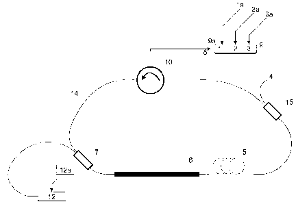
We first refer to Figure 1. The electrically tunable element considered in
figure 1 is
based on an electrically tunable Bragg grating and an electrically tunable
phase section.
In preferred embodiments the saturable absorber comprises a negatively biased
gain
section of a semiconductor laser cavity. In embodiments this cavity has three
sections
(1-3) as shown in the figure. The saturable absorber (section 1, controlled by
source la
in figure 1) used for mode locking can be integrated or separated from the
tuning
CA 02628923 2008-05-07
WO 2007/057713 PCT/GB2006/050396
12
components by using an additional circulator. The biasing of section 1 is
negative with
regards to ground potential, to provide (controllable) absorption.
The remaining sections are used for fine tuning the cavity length (section 2,
controlled
by source 2a) and for tuning the centre output wavelength (section 3,
controlled by
source 3a). The fine tuning (source 2a) can also be used to prevent "mode
hops". The
carrier offset frequency can be adjusted by changing the current (contact 12a)
to the
pump laser (12). (The order of elements 1, 2 and 3 shown in Figure 3 with
respect to
light incident via the circulator may be reversed (though this is less
preferable than the
arrangement shown).
Example details for the sections 1, 2 and 3 are as follows:
Gain section: Semiconductor optical material (such as InGaAsP, GaAs or InP)
with
optical gain (or optical absorption) at the relevant wavelength. The optical
gain is
provided by electrically exiting the carriers into higher energy states. This
absorption of
this is adjusted, for example experimentally, so that the frequency source
pulses.
Phase section: Semiconductor optical material (such as InGaAsP, GaAs or InP)
with
electrically (or optically) tunable refractive index. Electrically (or
optically) induced
changes to the refractive index changes the effective optical length.
Grating sections: Semiconductor optical material (such as InGaAsP, GaAs or
InP) with
electrically tunable refractive index, incorporating a frequency selective
element such as
a Bragg grating. Electrically (or optically) induced changes to the refractive
index
changes the effective frequency of the frequency selective element.
The source (12a) supplies the pump laser (12) which is used to excite the rare
earth ions
in the section of doped waveguide (6). The optical gain provided by the
excited ions is
used to create an optical field. The optical field does not reach a CW
(continuous wave)
lasing condition because the saturable absorber (1) prevents such a build up;
instead the
CA 02628923 2008-05-07
WO 2007/057713 PCT/GB2006/050396
13
system pulses. If required the resulting short pulse can further be compressed
in time
using a waveguide with negative dispersion properties (14). The pulsation
performance
and stability of the setup can also be improved by incorporating isolators in
the loop
and/or following laser 12, to prevent undesirable feedback (not shown in
figure 1).
We now refer to Figure 2. The optical comb generator shown in figure 2 is
particularly
well suited for monolithic or hybrid integration using "silica on silicon" or
other types
of integration technologies, in. particular photonic integrated circuit
technologies. The
low number of components and the (preferred) absence of any mechanical
components
(such as polarisation controllers) also make suitable for low cost optical
subassemblies.
Elements 4, the input from 12, 7, 17, 6 and, where present, 8, may be
implemented on a
single substrate; in a hybrid device either or both of the pump laser 12 and
the control
block 1, 2 and 3 may also be provided on the substrate. Although in
embodiments the
device may be entirely solid state, in variants the controllable frequency
selective
element may be implemented using a MEMS (micro electromechanical system)-based
adjustable grating, for example using a "MEMS based" micromechanical actuator
to
adjust the tilt of a small grating.
We now refer to Figure 3 (a variant of Figure 1). The optical comb generator
shown in
figure 3, (based on a figure 8 type layout), can be used to generate very
narrow pulses.
These narrow pulses generate an optical comb with a very wide frequency span
the
comb may therefore no longer require a "comb expander" as used to increase the
number comb lines.
We now refer to Figure 4 (a variant of Figure 1 with similar construction to
Figure 3).
The optical comb generator shown in figure 4, (based on a figure 8 type
layout), can be
used to generate very narrow pulses. These narrow pulses generate an optical
comb with
a very wide frequency span the comb may therefore no longer require a "comb
expander" as used to increase the number comb lines. The semiconductor control
element has been removed from one of the loops and therefore no longer
contributes to
pulse broadening. This results in an output with even narrower pulses / wider
comb
span.
CA 02628923 2008-05-07
WO 2007/057713 PCT/GB2006/050396
14
We now refer to Figure 5, which shows details of optical tuning of the optical
comb
generator.
Figure 5a shows injecting control light into the optical pump source changes
the carrier
concentration inside this device. Changes in carrier concentration will change
the output
power of the optical pump source and this can therefore be used to tune the
carrier
envelope offset frequency (fCeO).
Figure 5b shows injecting control light into the optical comb generator
control device
will change the carrier concentration inside this device. The associated
changes in
refractive index induced by carrier concentration changes will change the
effective
optical path length and the Bragg reflection wavelength. This control light
can therefore
be used to tune both the mode spacing (df) and / or the centre comb
wavelength.
Figure 6 shows an example practical application the optical frequency comb
generator,
for metrology, in which the optical comb is used for frequency downconversion.
The
output of the system is an RF signal that is locked to the frequency standard
(coinponent
1)-
The frequency of the frequency standard can be very high (in the THz or even
PHz
range). The stability, accuracy and phase noise properties of this frequency
standard are
maintained during the frequency down conversion process.
Descriptions of colnponents in figure 6:
1) Frequency standard with 2 outputs (fl and f2) at different frequencies:
Examples of such a frequency standard include a laser locked to absorption
dips in
gasses such as iodine, carbon monoxide, acetylene, methane, hydrogen cyanide
(and
many other gases). The second frequency of this standard could be a haimonic
of the
first frequency or alternatively it could be a second absorption dip in the
same gas.
CA 02628923 2008-05-07
WO 2007/057713 PCT/GB2006/050396
Altematively this frequency standard could also be a based on single trapped
ions or
atoms such as strontium, calcium or mercury.
In both cases the harmonic of the frequency standard could be generated using
harmonic
generation crystals such as (periodically poled) KTP or LiNb crystals.
2) Circuit for df frequency control. This circuit isolates (using filter(s))
the df
frequency and produces a control signal proportional to the frequency (or
phase) of df.
This control signal is used to drive the optical frequency comb generator and
to lock one
of the comb lines to f2.
3) Optical to electrical converter (such as a photodiode), this element also
acts as
non linear element for obtaining the mixing product ("i.e. beat term") of the
optical
input signals.
4) Solid state tuneable frequency comb generator (as described elsewhere in
the
patent), both the carrier envelope offset frequency (fc,o) and the mode
spacing frequency
(df) are adjustable. The output of this generator is an optical comb.
5) Optical combiner / optical coupler
6) Non linear comb expanding element used to increase the nuinber of comb
lines
such that the comb now also covers the first frequency (fl) of the optical
standard, as
illustrated in figure 6a. Examples of linear comb expanding elements include
microstructure fiber, photonic crystal fiber or (periodically poled) non
linear optical
crystals such as KTP and LiNb.
7) Circuit for &o frequency control. This circuit isolates (using filter(s))
the fCeO
frequency and produces a control signal proportional to the frequency (or
phase) of df.
This control signal is used to drive the optical frequency comb generator and
to lock one
of the comb lines to fl.
CA 02628923 2008-05-07
WO 2007/057713 PCT/GB2006/050396
16
8) RF up or down-converter, this circuit is used to increase or decrease the
RF output
frequency.
The operating principle is as follows: Using feedback loops that continuously
adjust the
input comb parameters (df and fCeO), two distinct comb lines (n1 an n2) of the
optical
comb generator are locked to the two optical components (fl and f2) of the
frequency
standard. The comb spacing frequency (df) can directly be used as the RF
output,
alternatively the RF up or down-converter (component 8) can be used to change
the RF
output frequency.
Embodiments of the frequency comb generator we have described can be used for
a
range of applications including, but not limited to: time generating systems,
metrology,
frequency down-conversion, bio medical imaging for example optical coherent
tomography, and telecommunications for example WDM (wavelength division
multiplexed) wavelength sources.
If desired, the frequency comb can be broadened by using non linear materials
such as
microstructure fibre, photonic crystal fibre or (periodically poled) non
linear optical
crystals such as KTP and LiNb.
No doubt many other effective alternatives will occur to the skilled person.
It will be
understood that the invention is not limited to the described embodiments and
encompasses modifications apparent to those skilled in the art lying within
the spirit and
scope of the claims appended hereto.