Note: Descriptions are shown in the official language in which they were submitted.
CA 02628942 2008-05-07
WO 2007/059446 PCT/US2006/060802
APPARATUS AND METHOD FOR
ANALYSIS OF OPTICAL STORAGE MEDIA
Cross-Reference To Related Applications
[0001] This non-provisional application claims the benefit of U.S. Provisional
Application
No. 60/735,331, entitled "Apparatus and Method for Analysis of Optical Storage
Media," filed
November 10, 2005, which is hereby incorporated by reference herein. This
application is
also related to U.S. provisional application no. 601865,197 entitled "Method
for Using Optical
Storage Media Analysis," filed November 10, 2006 (Dkt. no. 188641/US), which
is also
hereby incorporated by reference herein.
Field of the Invention
[00021 Aspects of the invention involve an apparatus and method for analyzing
the surface
of an optical storage medium. Aspects of the invention also involve an
apparatus and
method of determining if a given optical storage medium ("OSM"), of various
possible types,
can be processed in an optical storage device ("OSD"), of various possible
types, that can
read or write data to the OSM based on the detection of various possible
defects that can
prevent or inhibit processing. Various methods and apparatus conforming to
aspects of the
invention can be integrated into an existing OSD, can be integrated into a
standalone device
whose main purpose is to analyze OSM, and can be presented in other
embodiments.
Background
[00031 The information storage industry is driven by market demands to
increase continually
the capacity and performance of devices for storing information. One of the
needs is
distribution of information (spatial communication) to various locations and
retention of
information (temporal communication) to be accessed at a later time. One
popular
application for information storage is storage of video information, such as
movies, TV
shows, and home videos. Yet another popular application is storage of music
information.
Another application is the storage and distribution of software to end-users.
Driven by and
reflecting this market demand, a variety of storage formats have been
introduced into the
market to fill various needs.
[0004] There are numerous methods of storing information, such as through
printed matter
(e.g., books and magazines), semiconductor-based RAM and FLASH memories,
magnetic-
CA 02628942 2008-05-07
WO 2007/059446 PCT/US2006/060802
based MRAM or bubble memories, magnetic-based Winchester-type disc drives,
optical
storage using phase-change or prefabricated or "burned" media, and holographic
storage,
among others. There are certain advantages and disadvantages of each type and,
over
time, certain types of storage tend to dominate certain applications.
[0005] The compact disc ("CD"), a type of OSM, was introduced in the 1970s and
soon
became a popular method for storage and distribution of music information due
to certain
advantages it held over the then state-of-the-art (cassette tapes and LP
records). The CD
medium was also adopted for storage and distribution of computer software due
to certain
advantages it held over the then state-of-the-art (floppy discs). Further
advances in media
and CD recorder/player technology, types of readback devices, allowed
companies and
consumers to record their own CDs, using several different formats available,
to store
information of many types from music and video, to pictures and images, to
software and
data. The capacity of CDs varied but was on average around 600 MB per disc.
This was
sufficient for many applications, but was not adequate to store a motion
picture without
considerable compression.
[0006] The DVD (sometimes styled as Digital Video Disc or Digital Versatile
Disc although
the exact expansion (if any at all) of the acronym is not generally agreed
on), another type
of OSM, was introduced in the 1990s and quickly became popular for
distribution of pre-
recorded video information, such as movies and extra features. The DVD format
also allows
for storage and distribution of software and other forms of data. Further
advances in DVD
media and DVD recorder/player technology, another type of OSD, allowed
companies and
consumers to record their own DVDs to store information of many types from
music and
video, to pictures and images, to software and data. The capacity of DVDs
vary, some
DVDs have a capacity of about 4.7 Gbytes per DVD. This is sufficient to store
a full length
motion picture feature plus other information that is of interest and benefit
to consumers.
The adoption of DVD technology into the market was one of the most rapid
market
penetration stories of our time.
[0007] New technologies are now emerging to store even more data on an optical
storage
medium. For example, two new competing formats (others may emerge) are
popularly
referred to as Blu-Ray and HD-DVD. These formats can each store over 15 Gbytes
per
disc. This enables the storage and distribution of an HDTV-format movie on a
single disc.
Information storage using the principles of holography is also under
development. Other
2
CA 02628942 2008-05-07
WO 2007/059446 PCT/US2006/060802
improvements and formats will doubtless be introduced from time to time in
this competitive
market.
[0008] In general conceptual terms, the physical structure and operational
principles of most
optical storage methods is similar. Figure 1 is a partial side section view of
an OSM 10. For
the purposes of illumination but not by way of limitation, binary data is
encoded and
recorded onto the disc by differences in the height of the recording layer
(generally called
"lands" 12 and "pits" 14). Data may also be recorded using changes in the
phase of the
material, or other methods. The OSM includes a substrate 16 of acrylic or
other material. In
a phase-change based OSM, a layer of the appropriate material is inciuded in
the substrate.
In an OSM that uses difference in height, the pits and lands are encoded in
the substrate. A
protective coating 18, such as a polycarbonate, is applied over the substrate.
The coating is
optically transparent, at least for the wavelength of the laser used to read
the data encoded
from the pits and lands. An aluminized layer 20 may also be applied to the
substrate over
the pits 14 and lands 12. The aluminized layer improves reflection of the
laser from the pits
and lands. A label 22 may be on the substrate 18.
[0009] The laser is used to scan the disc and read back the data by detecting
the variation
in the reflected light. The data is stored in microscopic grooves or "tracks"
running in a
spiral around the disc. The OSD uses laser beams to scan these grooves, where
minuscule
reflective bumps (the lands) and non-reflective holes (the pits) aligned along
the grooves
modulate the laser signal which, when properly decoded, represents the zeros
and ones of
digital information.
[0010] DVD technology writes in smaller "pits" to the recordable media than CD
technology.
Smaller pits mean that the drive's laser must produce a smaller spot. DVD
technology
achieves this by reducing the laser's wavelength from the 780 nanometer ("nm")
infrared
light used in standard CD drives to about 625nm - 650nm red light.
[0011] Smaller data pits allow more pits per data track. The minimum pit
length of a single
layer DVD-RAM is 0.4 micron as compared to 0.834 micron for a CD.
Additionally, DVD
tracks are closer together, allowing more tracks per disc. Hence, track pitch--
the distance
from the center of one part of the spiral information or "track" to the
adjacent part of the
track--is smaller. On a 3.95GB DVD-R, track pitch is 0.8 microns; CD track
pitch is 1.6
3
CA 02628942 2008-05-07
WO 2007/059446 PCT/US2006/060802
microns. On 4.7GB DVD-R media, an even smaller track pitch of 0.74 microns
helps boost
storage capacity.
[0012] These narrow tracks require special lasers for reading and writing -
which can't
read CD-ROMs, CD-Rs, CD-RWs, or audio CDs. DVD-ROM drive makers solved the
problem by putting two lasers in their drives: one for DVDs, the other for
CDs. To facilitate
the focusing of the laser on smaller pits, DVD media uses a thinner plastic
substrate than do
CDs. Further, DVD media has a thinner protective coating that the laser must
pass through
to reach the pits to record or read data than does CD media. This reduction
originally
resulted in discs that were 0.6mm thick - half the thickness of a CD. Even
single-sided
DVDs have two substrates, even though one isn't capable of holding data.
Double-sided
discs with two data surfaces must be turned over to read data on each side. In
other OSMs,
the information can be stored as phase changes in the media, dye changes, or
in the
direction of magnetization in a magneto-optical storage medium, among others.
[0013] In various OSM, then, the data layer is protected by a protective
surface 18 that is
substantially optically transparent. In CDs and DVDs, it is typically a
polycarbonate material.
One of the significant problems that current users of optical storage media
face is damage
to the OSM protective surface. This can scatter or change the behavior of the
reflected or
transmitted light to the point that the data can no longer be read or written
or both. The
OSM error correction coding ("ECC") can handle errors of a certain size,
depending on the
OSD, but errors larger than that threshold cause the OSD to be unable to read
or write
through the damage. In DVD players, this can be manifested as skipping,
freezing, or an
inability to even recognize the DVD's presence. In CD pCayers, it can manifest
itself as a
high-pitched and annoying click, skipping, freezing, or an inability to even
recognize the
CD's presence. The frequency of this damage has been growing year over year as
the
rapid market penetration of OSM has reached relatively unsophisticated
consumers (e.g.
children) who do not treat the fragile protective surface with proper care.
[0014] Conventional methods exist to identify and alleviate problems reading
or writing data
to an OSM. Such conventional materials typically involve checking a data
stream read from
the OSM for errors, error correction code circuitry, and monitoring read retry
requests.
What is needed is a way to analyze the protective surface of an OSM. What is
also needed
is a way to determine whether data can be successfully read as well as written
to an OSM.
4
CA 02628942 2008-05-07
WO 2007/059446 PCT/US2006/060802
These and other needs are addressed by implementations and aspects of the
present
invention, as set forth in further detail below.
Summary
[0015] One aspect of the invention involves a method for analyzing the surface
of an optical
storage medium. The method includes the operations of directing at least one
light signal
on an outer surface of an optical storage medium. The optical storage medium
includes
encoded data. The method further includes detecting some portion of the at
least one light
signal reflected from the outer surface of the optical storage medium. And,
the method also
involves determining whether the encoded data may be accurately read as a
function of
detecting some portion of the at least one light signal reflected from the
outer surface.
[00161 Another aspect of the invention involves an apparatus for analyzing an
optical
storage medium. The apparatus, or "certifier," includes a platform configured
to support the
optical storage medium, which defines at least one side having a data layer.
The apparatus
further includes at least one light positioned to illuminate the at least one
side having a data
layer and at least one light detector positioned to receive light reflected
from the optical
storage medium and provide an output signal as function of the received
reflected light.
Finally, the apparatus includes at least one circuit eiement configured to
receive the output
signal from the light detector and to provide an output indicative of the
integrity of the at
least one side having a data layer.
[0017] These and many other aspects and implementations of the present
invention are set
forth in greater detail below.
Brief Description of the Drawings
[0018] Before explaining the disclosed implementations in detail, it is to be
understood that
the invention is not limited in its application to the details of the
particular arrangement
shown, because the invention is capable of other embodiments. Moreover,
aspects of the
invention may be set forth in different combinations and arrangements to
define inventions
unique in their own right. Also, the terminology used herein is for the
purpose of description
and not of limitation. Thus, the present invention is not intended to be
limited to the
embodiments shown but is to be accorded the widest scope consistent with the
principles
and features described herein including alternatives, modifications and
equivalents, as
CA 02628942 2008-05-07
WO 2007/059446 PCT/US2006/060802
defined within the scope of the appended claims. it is noted that the drawings
are not to
scale and are diagrammatic in nature in a way that is thought to best
illustrate features of
interest.
[0019] Figure 1 is a representative section view of an exemplary optical
storage medium;
[0020] Figure 2 is an isometric view of an optical storage media analyzer or
"certifier,"
conforming to aspects of the present invention;
[0021] Figure 3A is an isometric view of the optical storage media analyzer
set forth in Fig.
2, with a cover removed to illustrate various electronics and to show a
carrier, laser
assembly and detector assembly in a first position, which may be a starting
position of a
scanning operation;
[0022] Figure 3B is an isometric view of the optical storage media analyzer
set forth in Fig.
3A, with the cover removed to illustrate various electronics and to show the
carrier, laser
assembly and detector assembly in a second position, which may be an ending
position of a
scanning operation;
[0023] Figure 4 is a section view taken along line 4-4 of Fig. 2;
[0024] Figure 5 is a flowchart illustrating one method of analyzing an optical
storage media,
confirming to aspects of the present invention;
[0025] Figure 6 is a diagram illustrating a laser incident on an optical
storage media, a
reflection of the laser off a defect on the optical storage media, and the
collection of some
portion of the reflected laser off the defect by a detector;
[0026] Figure 7 is a block diagram illustrating the electronics of the
analyzer shown in Fig.
1, conforming to aspects of the present invention;
[0027] Figure 8 is a diagram illustrating a laser reflected from an
unblemished surface of an
optical storage media and incident on an optical sphere detector in accordance
with aspects
of the present invention;
6
EF==~=,~ =~= y~ E ,y yy S rS.'. ihn ~. [~ ~ ~Ã 4t1~3 " Y. ...-SYSi
CA 02628942 2008-05-07
WO 2007/059446 PCT/US2006/060802
[00281 Figure 9 is a diagram illustrating a laser reflected from a blemished
surface of an
optical storage media and incident on the optical sphere detector of Fig. 8,
in accordance
with aspects of the present invention;
[0029] Figure 10 is a diagram illustrating a laser reflected from an
unblemished surface of
an optical storage media and incident on an optical sphere detector with a
masked aperture,
in accordance with aspects of the present invention;
[0030] Figure 11 is a diagram illustrating a laser reflected from a blemished
surface of an
optical storage media and incident on the optical sphere detector as shown in
Fig. 10, in
accordance with aspects of the present invention; and
[0031] Figure 12 is an isometric view of certifier components integrated with
a DVD read
back device, in accordance with aspects of the present invention.
Description of Embodiments
[0032] Embodiments conforming to aspects of the invention may involve a method
and
device for analyzing and inspecting the surface of optical storage media
("OSM") to
determine the topographical properties of the surface. Particularly,
embodiments can detect
the absence or presence of features on a given OSM, commonly referred to as
defects,
such as, but not limited to, scratches, dings, dust, dirt, fingerprints, other
organic or
inorganic material, bends or creases, cracks, or other foreign objects
partially or fully
embedded in or resident upon the surface. The presence of such surface defects
can, in
some instances, affect the ability of an optical storage device ("OSD") to
read or write data
from or to the OSM.
[0033] As such, embodiments conforming to aspects of the invention can be
configured to
determine if the presence, size, or prevalence of the defects are such that an
OSD can or
cannot read or write the data reliably. The analysis may also be conducted to
determine if
some, but not all, OSD can read or write the information. Moreover, the
analysis may take
into account a particular type of OSD or OSM and determine the likelihood of
reliable data
extraction or data addition from or to the particular OSD and/or OSM.
Embodiments of the
invention may further be configured to determine and identify the type of a
defect so that a
user can respond appropriately. OSM that can be characterized, analyzed,
and/or inspected
by embodiments described herein include by way of example, but are not limited
to, DVD,
7
CA 02628942 2008-05-07
WO 2007/059446 PCT/US2006/060802
DVD-ROM, DVD-R, DVD/R-W, DIVX, DVD-Audio, CD, CD-ROM, CD-WORM, CD-R/W,
SACD, Blu-Ray, HD-DVD, game discs, holographic, and other types of optical
storage
media that may be developed in the future from time to time.
[0034] Unlike conventional, so-called "direct data" methods for measuring the
read back
quality of an OSM, embodiments described herein do not only rely on reading
the data in
order to compare it, checking the data stream for errors, using error
correction code
circuitry, or monitoring read retry requests from a player; rather,
embodiments conforming to
aspects of the invention can analyze the protective surface of an OSM to
determine if the
surface will prevent or inhibit the data from being read or written. These
conventional
methods, however, may be used to supplement the surface technique and
implementation
set forth herein. Conventional methods offer no known way of determining if
the OSM can
be successfully written, other than verifying the written data by reading it
back.
[0035] Surface analysis techniques and configurations conforming to aspects of
the
invention are not optimal to detect defects in the data layer, which lies
beneath the
protective surface, but because these are rarer than defects in the exposed
surface of the
OSM, the compromise is acceptable. The data is stored in the reflective pits
and non-
reflective landings and covered with a protective coating. It is the exposed
protective
surface that gets scratched, smudged, dented, or otherwise damaged. These
defects
diffract the laser light from the OSD player and obscure the data layer
beneath, thereby
making it difficult to read or write the data layer. Nonetheless, as some
portion of the light
transmitted on an OSM will transmit through the outer layers, including the
protective
coating, and to the data layer, surface analysis implementations conforming to
aspects of
the invention may be configured to detect defects in the data layer, either
alone or in
conjunction with detecting defects in the outer layers.
[00361 Surface analysis may be employed alone or in combination with
conventional direct
data analysis techniques. In combination, surface analysis techniques and
direct data
analysis may determine data read capability despite extensive surface defects.
Surface
analysis technique and apparatus described herein canoffer much increased
speed over
conventional direct data error detection methods that actually read the data.
Embodiments
may also analyze the surface characteristics of an OSM to determine the nature
of the
defect and recommend corrective action. Various embodiments can be used singly
or jointly
to good effect.
8
CA 02628942 2008-05-07
WO 2007/059446 PCT/US2006/060802
[0037] Figures 2-4 illustrate one particular example of an optical certifier
apparatus 100
conforming to aspects of the invention. The optical certifier includes a body
structure 102
supporting a spring-loaded cover 104 that is positioned to cover an OSM stage
106 where
the OSM 108 is positioned by a user. This implementation is configured to
analyze surface
defects of a DVD or CD type OSM. Accordingly, the stage includes a hub 110
that receives
a central aperture of conventional DVD, CD or the like. The hub is attached to
a motor 112
(see Figs. 3A, 3B) that rotates the hub. The stage, hub, and related structure
may be
referred to as an OSM support and movement assembly. The OSM motor is adapted
to
rotate the hub supporting the OSM at a desired speed, such as 600 revolutions
per minute
(rpm). This motor may be equipped with a speed sensor to communicate when it
is up to
the desired speed, such as 600 rpm. The stage 106 further includes a window
114
positioned such that light from a light source 116 may be shown on the surface
of the OSM
108 positioned on the stage, and reflected light captured by a detector 118.
[0038] Referring particularly to Figs. 3A, 3B, and 4, the optical certifier
100 further includes
a light generation and detection assembly and processing electronics. In the
particular
configuration of Figs. 2A-4, the light generation and detection assembly 120
includes one or
more lasers 122 or other light sources 116 arranged to be directed through the
window 114
at the surface of an OSM supported on the stage. The light generation and
detection
assembly further includes one or more detectors 118 arranged to detect the
light reflected
from the surface of the OSM.
[0039] In the particular arrangement of Figs. 2-4, both the laser and the
detector are
supported on a carrier 124. The carrier is moveably supported so that it may
be moveably
positioned relative to the OSM. In this particular configuration, the carrier
is arranged to
move radially with respect to the OSM 108 positioned on the hub 110. The
carrier is
supported on two rails 126, 128. Adjacent one rail 126, a worm gear 130 is
coupled with a
motor 132. A gear 134 is coupled with the carrier so that rotation of the worm
gear moves
the carrier.
[0040] On one side of the carrier 124, the laser 122 is coupled to the
carrier. The laser is
positioned to transmit light through the window 114 on the surface of the OSM.
On the
opposite side of the carrier, in this particular implementation, adjacent the
worm gear 130, a
printed circuit board 136 supports at least one detector. The PCB positions
the detector(s)
118 to be positioned in the path of reflected light from the OSM. Arranged as
shown in Figs.
9
;a~h [}sN 4arr P M?:rM Ã~Xlk*.~F~t~.!1'::l.~l
CA 02628942 2008-05-07
WO 2007/059446 PCT/US2006/060802
2-4, and discussed further below, rotation of the worm gear causes the laser
and the
detector to be scanned across the surface of the OSM. In Fig. 3B particularly,
the light
generation and detection assembly 120 is shown in phantom in an outer
orientation, and
also shown at a second position closer to the hub. This movement allows the
laser to scan
the OSM surface from its outer edge radially inward toward the inner aperture
(hub).
[0041] In an alternative implementation, the laser/detector assembly is
mounted on a
pivoting bearing and configured to scan the OSM in an arc. in yet another
alternative, the
laser and detectors are mounted on separate assemblies that are moved
substantially
contemporaneously. Further, a light source that is adequately focused or
adequately
collimated or both is used to illuminate the surface of the OSD instead of a
laser.
[0042] Aspects of the processing electronics are described in greater detail
below with
respect to Fig. 7. Output from the processing electronics is transmitted to a
display 138,
such as an LCD, positioned at the front of the certifier.
[0043] Figure 5 is a flowchart illustrating one particular method of analyzing
an OSM
surface to determine whether defects are present and whether the defects will
affect
readback or writing of data. To begin, an OSM is placed in the certifier on
the hub and the
motor is started to cause the OSM to rotate (operation 200). In one particular
arrangement,
the certifier 100 includes the lid 104 to at least partially cover the OSM and
light source 116,
detector 118, and other components during testing. The lid shields the
detector assembly
from ambient light to improve the signal to noise ratio. It also functions as
part of an
interlock system to protect the user's eyes from the laser. Alternatively, the
OSM support
and movement assembly, may be supported on a moveable tray that retracts the
OSM
support and movement assembly within an enciosed area and positions the
assembly
relative to the laser assembly. In either configuration, when the lid is
closed or the tray
retracted, a switch operatively coupled with the lid or tray, transmits a
signal to an OSM
motor controller which controls the spindle motor 112 causing it to start and
rotate to the
OSM at a set or variable speed. Alternatively, it is also possible to include
a manually
activated switch to cause the motor to activate and run at some speed. The
certifier
includes a power switch 140 which provides power to the device when switched
on. It is
also possible to include computer control or some other arrangement to cause
the motor to
activate.
;tt Ea
CA 02628942 2008-05-07
WO 2007/059446 PCT/US2006/060802
[00441 Next, the motor speed is maintained to determine when the proper speed
is reached
(operation 210). In one embodiment, the spindle motor spin acceleration is
monitored and
used to determine the size of the disc under test, including whether there is
no disc in place.
For example, the motor will accelerate faster with no disc in place than with
an
approximately 8 cm game disc, such as a GameCubeT"' disc, under test which
will in turn
accelerate faster than an approximately 12 cm disc, such as a DVD. This
information can
be used to customize the type of test performed on the disc, including the
thresholds used
for damage detection, the equations used for damage score determination, or
the amount of
area scanned, among others.
[0045] When the desired speed is reached, the carrier motor 132 is activated
to move the
light source and detector assembly 120 so that the one or more light sources
successively
illuminates a spot or spots at various locations on the spinning OSM
(operation 220). The
light source/detector carrier 124 is moved so that, as the disc spins, the
surface of the
optical storage medium is in turn illuminated until the entire surface or a
portion thereof has
been sampled by the light source. In another embodiment, the carrier motor 132
is
synchronized with the spindle motor 112, for example, by use of a once-around
sync
generated by the OSM motor, so that the carrier motor advances at a rate,
which could be
continuous or stepwise, determined by the spindle motor spin speed. In this
case, the
carrier motor can be activated while the spindle motor is accelerating,
decelerating or at a
variable speed and still successively illuminate the entire surface, or the
desired portion of
the surface, of the OSM. In one embodiment, for the minimum possible test
time, the motor
is continuously accelerated and then continuously decelerated to a stop such
that the scan
of the entire surface, or desired portion thereof, is completed just as the
spindle motor
comes to a stop. In the method of Fig. 5, the carrier moves until it has
scanned the entire
OSM surface, which is detected by reaching a radial endpoint near the hub. In
any event,
the certifier is configured to scan the surface and determine when the scan is
complete
(operation 230).
[0046] The reflection off the surface, depending on the presence or absence of
defects, is
directed toward or away from the detector, which in one particular
implementation may be a
photodiode. The surface of the OSD could be scanned in its entirety or
partially. It can also
be scanned once or multiple times before outputting the results, if desired.
After the scan is
completed, the motor turns off and brings the spinning OSM to a halt
(operation 240).
11
<M;;
CA 02628942 2008-05-07
WO 2007/059446 PCT/US2006/060802
[0047] As will be discussed in greater detail below with respect to Figs. 6
and 7, the detector
and processing electronics are configured to detect the reflected light,
generate and output
voltage, and compare the output voltage to a threshold voltage in one
particular
arrangement (operation 250). The threshold voltage is set to the output
voltage associated
with a certain level of surface defects that will affect proper OSM read back.
The threshold
voltage may be OSM type specific, OSD type specific, and related to other
factors.
Exceeding or not exceeding the threshold causes the appropriate LCD display,
such as
"pass" and "fail," respectively, or the like (operation 260).
[0048] Referring now to Fig. 6, as well as other figures, the surface analysis
technique is
described in greater detail. The reflection of light 142 from a source 116 off
a smooth
unblemished surface 144 (no defect present in the illuminated area) of an OSM
108 is along
a path 146 referred to as the principal axis (dashed line). In one particular
arrangement, the
detector assembly is arranged such that the light along the principal axis
does not intercept
a detector 118, so there is no signal to the electronics when the light is
incident on an
unblemished surface. When a defect 148, such as a scratch, is in the beam spot
along the
principal axis from the light source, the light is scattered from the surface
and the path 150
of the reflected beam deviates from the principal axis. In one arrangement,
the detector or
detectors are arranged such that the scattered reflection from a defect will
generally
intercept a light-sensitive detector, thereby producing a signal that is
detected by associated
electronic circuitry, discussed in further detail below with respect to Fig.
7. It is possible for
some defects to scatter light in a direction such that it is not intercepted
by a detector. In
this case, the defect would not be detected. This likelihood can be reduced by
utilizing more
detectors arranged around the principal axis, or by using a ring or partial
ring of detectors, or
a single detector of sufficient size (with the area that intercepts light
along the principal axis
masked out) that light that deviates from the principal axis intercepts the
detector, or by
using a photodiode with many light-sensitive pixels or a charge-coupled device
that detects
light on its many photosites or pixels, or by other methods.
[0049] The example illustrated in Fig. 6 employs a single laser 122 and
associated optical
detector 118, arranged to direct a laser to the surface 144 of the OSM 108 and
collect the
reflected light, or some portion thereof. Since defects can scatter incident
light in various
directions depending on their morphology, increased likelihood of detecting
defects can be
achieved by adding one or more lasers that intersect the OSM surface at a
different incident
direction or angle or both to the first laser or splitting the output of one
or more light sources
12
tEnF:iMÃ4=%t~,;N'P}, + ,
CA 02628942 2008-05-07
WO 2007/059446 PCT/US2006/060802
and directing the outputs to intersect the OSM surface at the same or a
different incident
direction or angle or both. Increased likelihood of defect detection can be
achieved by
adding one or more light-sensitive detectors at the same or different
reflected direction or
angle or both to the first light sensitive detector.
[0050] In the particular certifier illustrated in Figs. 2-4, two detectors
(118A, 11 8B) are
arranged in a plane perpendicular to the direction of the principal axis 146
but at right angles
to each other. Such an arrangement provides adequate sensitivity for certain
purposes to
detect defects oriented in random directions, including purely radial or
purely circumferential.
[0051] Figure 7 illustrates an electrical diagram for a certifier employing
two detectors,
which may or may not be arranged in a plane perpendicular to the direction of
the principal
axis but at right angles to each other. With the removal of one detector, the
electrical
schematic is substantially similar to that of a certifier employing one
detector.
[0052] Referring again to Fig. 6, it is also possible to arrange a detector
152 (shown in
phantom) along the principal axis and calibrate the system such that the light
source,
reflected off an unblemished, defect free surface, and impinging on the
detector produces a
known output signal. When a defect, such as a scratch, is in the area sampled
by the
illuminated area, the light is scattered from the surface and the path of the
reflected beam
deviates from the principal axis 146. This will lead to a reduction in the
amount of light
illuminating the detector 152 and a corresponding reduction in the output
signal from the
detector. These deviations from the known output may then be used to determine
the
presence of a defect. It is possible to arrange a certifier with an on axis
detector 152, one or
more off axis detectors 118, and combinations thereof.
[0053] The detector may take on various forms. A charge-coupled light
sensitive device
("CCD") of sufficient size with multiple photosites or pixels can have the
light impinge on
certain photosites that are placed to intercept light along the principal
axis. When the light is
scattered by a defect in the surface, the photosites that intercept light
along the principal
axis will see a reduction in the amount of illumination and the photosites
that are along the
scattered path will see an increase in illumination as the light scatters off
the defect. Such a
detector integrates both on axis and off axis advantages.
[0054] Similarly, instead of a CCD with multiple photosites, multiple
photodiodes, with one
or more placed on-axis and one or more placed off the principal axis, could be
used. If
13
:w~~ M.}'rr!if~~ ~y~kN ~s.~~-
CA 02628942 2008-05-07
WO 2007/059446 PCT/US2006/060802
some or all of the scattered light is scattered such that it does not
intercept the pixels that
are not on the principal axis, then the off-axis detectors would not produce a
signal, but the
on-axis photodiode or diodes would see a reduction in the amount of light
illuminating them
and, correspondingly, produce a lower output signal.
[00551 In some embodiments, the reduction in the light illuminating the on-
axis detector
assembly due to a defect may be too small a fractional change in the overall
illumination and
the on-axis detector signal change will be small. In this case, the off-axis
detectors can still
show a signal that can be acceptably reliably detected. Therefore, off-axis
detector, on-axis
detector, or some combination thereof may be usefully employed in embodiments
conforming to aspects of the present invention.
100561 As shown diagrammatically in Figs. 8-9, it is also possible to use an
integrating
optical sphere 156 to gather the scattered light 150 from the laser 116. In
one arrangement
shown in Fig. 8, the sphere includes an aperture 158 that is arranged
adjacent, but not
along, the principal axis 148. Accordingly, as shown in Fig. 9, when the light
encounters a
defect on the OSM 108, some portion of the light 150 scattered from the defect
will be
directed into the aperture. Internally, the sphere reflects the light and
provides an output
commensurate with the detected light. Similar optical methods for gathering
light can be
employed in embodiments conforming to aspects of the present invention. For
example, a
single detector could be used but in conjunction with a reflective surfaces or
surfaces, or
refractive surface or surfaces, or both to collect the light scattered by the
damage and direct
it to the single detector. As shown in Figs. 10-11, the integrating optical
sphere may include
a mask 160 on the principal axis such that light along the principal axis does
not enter the
sphere but light 150 that has been scattered from a defect does enter the
sphere to be
detected. In this example, the aperture is open on all sides around the mask,
and hence
around the principal axis. In the first sphere example, the entire aperture is
located off-axis,
thus light scattered to the opposite side of the principal axis may not be
detected.
[0057] Referring again now to Fig. 7 and others, the OSM motor 112 and
laser/detector
assembly motors 132 are controlled by respective controllers (162, 164). The
spin motor is
responsive to the lid switch, tray switch, or manual switch, and may also
require a
verification that the lid or tray is in a lock position, which may also be
provided from a signal
from a switch, separate or the same as the lid or tray switch and an interlock
signal (166,
168). Laser 122 illumination may be triggered from the OSM motor controller,
the
14
CA 02628942 2008-05-07
WO 2007/059446 PCT/US2006/060802
laser/detector assembly motor controller, or by other means. The laser or
other light source
impinges on the OSM 168 surface and light reflected therefrom intercepts one
or more
detectors. The detectors (118A, 11 8B) generate output voltages (170) as a
function of the
amount of incident light which may be just the noise level voltage if there
are no defects
causing light to be incident on the detectors. The output voltage is
transmitted to one or
more amplifiers and/or filters 172. The amplifier or amplifiers are coupled
with one or more
associated comparator circuits (174A-174D). Each comparator circuit is
provided with a
reference voltage (176A-176D). Further, each comparator circuit is coupled
with one or
more light emitting diodes ("LEDs") or other output devices.
[0058] In the particular arrangement of Fig. 7, the output from the detectors
is coupled with
four comparator circuits. Each comparator circuit has a unique threshold
voltage. Further,
each comparator circuit normally drives a green LED, and upon meeting the
threshold drives
a red LED (LED outputs 178A-178D). Alternatively, each comparator output is
arranged to
drive a respective LCD display, as "Pass," Some Damage But Will Piay", "Fail
Level 1," "Fail
Level 2," and "Fail Level 3."
[0059] When the laser 122 is incident upon a defect, the light is generally
briefly intercepted
by the light-sensitive detector(s) 11 8A, 11 8B which produces the output
voltage 170. This
detector voltage signal is summed and amplified by the amplifier 172 and,
using the
comparator circuitry 174, is compared to the reference voltage(s) 176. In one
particular
implementation, if the reference voltage is exceeded, then a red LED is
illuminated and a
green LED is turned off to signal to the user that this reference voltage has
been exceeded.
It has been found that there is an approximate and sufficient correspondence
between the
amplitude of the detector signal and the likelihood that the defect that
scattered the light that
created the corresponding signal will prevent a DVD from playing accurately.
[0060] One or more comparator circuits, using the same or different reference
voltages,
coupled with a green and red LED pair, can be used to provide an approximate
scale of
damage. If the red LEDs corresponding to the higher reference voltages are
triggered, then
it has been found that it is likely that a more extensive defect is present,
which in turn
indicates that the defect is more likely to interfere with proper read back of
the OSM and
correction of the defect is more difficult.
CA 02628942 2008-05-07
WO 2007/059446 PCT/US2006/060802
[0061] The reference voltages to the comparator circuits can be fixed or can
be adjusted by
the user. In one embodiment, a single comparator circuit with an adjustable
reference
voltage controlled by a potentiometer or similar device accessible to the user
can generate
the same approximate scale of damage by testing the OSM multiple times with
different
reference voltages. In another embodiment, the reference voltage is provided
by a digital to
analog converter and set via a software update from an attached computer or
other device.
In another embodiment, the digital reference level is compared to the computed
damage
level inside the microcontroller or DSP controller.
[0062] In another embodiment, the resulting damage level is displayed on the
LCD screen
138 based on the output from the comparators. In yet another embodiment, the
damage
level is outputted to a separate device, such as a personal computer or point-
of-sale
terminal, using a interface such as USB 2.0 and displayed on the separate
device.
[0063] In one'particular certifier implementation, a DigiKey model no. 38-1
000-ND laser and
Hammamatsu model no. S1787-08 Photodiode detectors are employed. The first
comparator 174A has a 1 V reference voltage, the second comparator 174B has a
2 V
reference voltage, the third comparator 174C has a 3 V reference voltage, and
the fourth
comparator 174D has a 4 V reference volt. Based on a correlation to several
DVD players
currently available in the market used as references, such as Philips DVP642,
Samsung
DVD-L70, Hitachi DVP755U, or Sony DVP-NS575P/S, it has been determined that an
amplified photodiode output between 1 and 2 volts, which would cause
illumination of the
red LED 178A by the first comparator circuit, but would not illuminate the
second through
fourth LEDs 178B-178D indicates that the DVD being analyzed would play on
these players,
but some defects are nonetheless present. A voltage of 2 volts or greater,
illuminating the
second 178B through fourth 178D red LEDs, depending on the voltage, indicates
that the
subject DVD has defects sufficient to inhibit or prevent play of the DVD on
these reference
players. Increasing output voltage generally corresponds with a greater degree
of defect.
The particular threshold voltage or voltage for any particular implementation
can depend on
various factors, including the type and power of laser employed, the output
voltage of the
detector employed, the type and amplification range of the comparator
arrangement
employed, if any. Further, the threshold values may be optimized in any
particular
arrangement depending on the type of OSM, the type of protective coating, the
type of
expected use, customer issues, as well as other factors.
16
CA 02628942 2008-05-07
WO 2007/059446 PCT/US2006/060802
[0064] In other embodiments, the amplified signal from the detector can also
be integrated
to provide an approximate measurement of the total amount of damage present on
the disc.
In another embodiment, the comparator circuitry 174A can also be monitored by
an optional
counter so that the number of defects exceeding the given threshold or
thresholds can be
measured. In another embodiment, the output signal can be analyzed by a peak
sample-
and-hold circuit that outputs the peak signal detected until it is reset. This
peak signal can
be converted using an analog-to-digital converter and output as a voltage, it
can be used to
drive an analog dial or needle indicator, or other methods.
[0065] In another embodiment, the output from the detector arrangement, or a
portion
thereof, can be digitally sampled, analyzed, and output in a number of ways
that will be
obvious to those skilled in the art. In one particular certifier
implementation, two detectors
are placed off-axis and orthogonal to each other. In one particular
implementation, the
detectors are OsramTM model BPW34S or FairchildTM QSB34CGR detectors. The
amplified
signal is routed to a digital signal processing ("DSP") chip, such as Texas
Instruments 32-bit
Fixed Point DSP TMS320F2808, which is operating at an analog input sample rate
of 20
kHz. The signals are fed separately to two analog inputs on the DSP and a
"damage level"
computed as follows:
Damage level = {A*(V1) + B*(V2)} / M
where V1 and V2 are the digitized voltage from the detectors and A, B, and M
are adjustable
parameters dependent on the desired weighting of the voltage from each
detector. - In
another embodiment, the damage level is computed as follows:
Damage level = square root { A*(V1)~2 + B*(V2)"211M
In either event, the damage level is displayed for the user. The weighting
values can be
determined by the relative importance of the defects that scatter light to
each detector or
based on a calibration of detector sensitivities, or both, or for other
reasons. For example,
each detector does not necessarily produce the exact same output signal as
another
detector for the same given illumination. By weighting the digitized voltage
of the detectors
accordingly in the damage level calculation, this effect can be reduced to an
acceptable
level for each application.
17
7 AN ~'WVJNM
CA 02628942 2008-05-07
WO 2007/059446 PCT/US2006/060802
[0066] In addition, for various OSM, the orientation of a defect can be
related to the
likelihood that the data will not be read. For example, in a typical DVD
player, a defect that
proceeds circumferentially around the disc, thereby rendering unreadable a
long successive
or interleaved section of data, is more likely to result in uncorrectable
errors than a radial
scratch that periodically obscures a shorter portion of data. In this case, it
is desirable for
the damage level to be higher for a defect that is circumferential or
substantially
circumferential than a similar defect that is radial or substantially radial.
This damage score
can be normalized and rounded or truncated for convenient display.
[0067] In one embodiment, the highest damage level measured is outputted to
the user via
the LCD 138 or communicated to an external device such as a PC or point-of-
sale terminal.
In another embodiment, the number of events where the damage level exceeded a
certain
threshold or thresholds can be outputted. In another embodiment, the signal
can be
integrated over the entire signal, or a portion thereof, and the resulting
value used as a
measure of overall damage. The damage level as a function of location on the
disc can be
recorded and displayed in the form of a map of the OSM showing damaged or
undamaged
areas. The damage level can be related to the amount of repair required to
reduce the
damage level to a defined threshold and the amount of repair required can be
displayed, It
is also possible to continually output the damage level for analysis or
display. In yet another
embodiment, the signal is not analyzed by the DSP but stored and transmitted
to another
device, such as a computer or disc polishing device, for analysis.
[0068] In cases where a plurality of detectors is used, the damage level can
be computed
as:
Damage level = square root { A*(V1)~2 + B*(V2)"2 + C*(V3)A2 + D*(V4)~2 +.....}
/ M
Damage level ={ A*(V1) + B*(V2) + C*(V3) + D*(V4) +.....} / M
[0069] In another embodiment with an on-axis detector and two off-axis
detectors, the
signal from the off-axis detectors can be subtracted from the on-axis
detector. When light is
scattered by damage, the voltage at the on-axis detector is reduced and the
voltage at the
off-axis detector is increased. By mathematically combining these two changes -
the
reduction in voltage at the on-axis detector and the increased voltage at the
off-axis
detector, the signal to noise ratio at the analyzing electronics can be
increased.
18
CA 02628942 2008-05-07
WO 2007/059446 PCT/US2006/060802
[00701 Other equations for computing a damage level from the digitized sample
from one or
more detectors can be -used in implementations conforming to aspects of the
invention. The
on-axis detector signal may arranged to vary with the reflectivity of the
disc. A surface that
is more reflective will result in a higher average voltage produced by the on-
axis detector.
This varying signal, possibly in conjunction with the disc size information
determined as
discussed above, can be used to determine which type of disc (for example, Blu-
Ray, HD-
DVD, DVD-ROM, game disc) is being measured and customize the type of test
performed
on the disc, including the parameters used in the damage score, the thresholds
used for
damage detection or for pass/fail determination, the equations used for
computing a
damage score, or the amount of area scanned, among others. In some discs
designed to be
recorded by users, the recorded data changes the reflectivity of the
underlying surface., This
change in reflectivity can be used to identify areas with data and areas
without data. A
defect in an area without data is not detrimental to readback as is a defect
in the area
without data. On the other hand, a defect in an area currently without data is
detrimental to
writing additional data to the disc. For example, some game discs, such as
certain Sony
PlaystationTM 2 discs, have a black surface instead of a shiny aluminized
surface to store
the data. Since a dark surface will absorb more light than a shiny one, the
amount of light
that is reflected is reduced. Correspondingly, the amount of light that is
scattered from a
defect on a black game disc is also reduced compared to the light that would
be scattered
from a similar defect on a standard DVD disc. The threshold for the damage
level needs to
be changed to account for this change. When a dark coated disc is measured,
the signal
from an on-axis detector will be reduced compared to the signal produced by a
standard
shiny DVD. This reduction in signal can be used to identify the type of disc
in the player.
The measurement process, the damage level calculation, the damage level
thresholds can
all be customized with this information.
[00711 Embodiments may be provided in a standalone device or "optical
certifier" that can
rapidly analyze an OSM surface. Such a standalone device might be suitable for
a company
that rented DVDs or other OSM or otherwise allows access to consumers or other
third
parties, to ensure that their inventory of DVDs would play or allow data
access properly
when the consumer uses them. An optical certifier can additionally be
integrated into the
company's computerized inventory or point-of-sale system to record the damage
history of
the OSM or the history of the consumer in damaging OSMs. Further, the
thresholds could
be set for each particular customer as the company received feedback from them
and
determined that their OSD was particularly sensitive or robust in regard to
reading or writing
19
r ~r~~i
hfiEr.a N
CA 02628942 2008-05-07
WO 2007/059446 PCT/US2006/060802
through defects. This standalone device would incorporate a motor to spin the
disc, a
method for scanning the laser or lasers along the radius of the disc as it
spins, and circuitry
to make the measurements, as discussed above.
[00721 Methods and configurations set forth herein can also be integrated into
an existing
OSD, such as a DVD player/recorder or CD player/recorded, to scan the disc
before starting
the playback or write sequence to determine, in advance, if the disc can be
read or written
all the way through, or whether some defects may affect data access or
storage. This might
be advantageous, for example, to a company making DVD players.
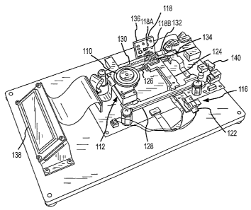
[0073] One example of an integrated player/certifier is illustrated in Fig.
10. This integrated
device could include some or all the features of the stand-alone device or,
more
advantageously, use certain features already existing in the OSM read back
device, such
as, but not limited to, the OSM motor, the OSM support, the laser slide
assembly, the laser,
the optics, such as the lens, the detector, and various features of the
electronics. In one
exemplary embodiment for an OSD such as a DVD player, a separate laser and
detector
assembly are added to the existing laser slide assembly as shown in Figure 10.
[00741 More particularly, the alternative certifier 180 implementation
includes the laser 122
and detectors 11 8A and 11 8B (and related PCB 136) mounted on a conventional
DVD
player laser assembly 182. The laser assembly is mounted on opposed rails 184,
186. The
conventional DVD read write laser 188 is supported in about the middle of the
laser
assembly, with the laser 122 and detectors 118 at either end. Only a portion
of the
assembly is shown, for ease of reference the aperture 190 is axial arranged
with a
conventional DVD player motor and hub. Accordingly, the rails are positioned
to move the
laser assembly radially with respect to a DVD mounted in the device. A motor
192
operatively coupled with a worm gear arrangement 194 moves the laser assembly
182, and
hence the laser 122 and detectors 118A and 188b, back and forth along the
rails.
[00751 It is also possible to use the conventional laser 188 is a dual role of
certifier laser and
read/write laser. In such an arrangement, either the laser orientation is
altered to so that
some light reflected from a defect is scattered to the detectors 118, or the
detectors are
rearranged to detect light reflected from a defect with the illustrated
positioning of the laser
188. Other possible laser or detector arrangements are also possible that
provide for dual
user of the read/write laser.
>...t:. . ,,.,
;k~~W,.~:~,~..:. ~:~,~
CA 02628942 2008-05-07
WO 2007/059446 PCT/US2006/060802
[00761 A comparator circuit such as that described in Figure 7 is added to the
existing
electronics. In this embodiment, the OSM is spun up by the DVD player motor,
the DVD
laser slide 182 is moveably actuated across the disc, the separate laser 122
is energized
and the output from the separate detector assembly 118 is monitored by the
comparator
circuit to signal the OSD whether the OSM can be accurately read or written.
The threshold
can be customized for the capabilities of this particular OSD rather than the
stand-alone
certifier case where the thresholds are generally, but not necessarily, set to
accommodate
the characteristics of a variety of OSDs. The thresholds for successful read
back and
successful writing can be either the same or different.
[00771 Methods and/or devices that can repair certain types of damage on OSM
exist.
Equipment used for repairing damaged discs generally uses different repair
methods,
including different time spent performing the repair method, depending on the
nature of the
damage. Often the different types of methods are codified into fixed programs
that the user
can select. In some cases, the different types of methods may have variable
parameters,
such as the time of each abrasive or polishing operation that the user can
select. It is
desirable to select the program that will repair the defect to a certain
minimum level of,
playability, but not remove more material than is necessary to maximize the
number of
repairs that can be performed on a given disc before the protective material
is entirely
removed. In OSM-based businesses that utilize repair systems, the decision on
which of the
methods or parameters is suitable for a given defective disc is a recurring
problem.
Typically, the decision is made by visual inspection. The several
disadvantages in this
approach are that different people may judge the required repair differently,
that they may
judge the required repair incorrectly, leading to an over-aggressive repair or
an incomplete
repair, and the recurring cost of training employees to make said
distinctions. In one
embodiment, the OCD be used to quantify the nature of damage and may then be
configured to measure the disc and display the proper method or program via a
display
method such as LCD readout or display screen or, even more advantageously, can
communicate directly with the repair equipment to set the proper program to
achieve a
certain level of repair. After the repair, the OCD can be used again to verify
that the repair
or cleaning was successful.
[0078] In another embodiment, the automated repair system that takes a stack
of unsorted
discs, the OCD module measures each disc and determines the appropriate repair
program,
then the repair module executes the given program, and then passes the OSM to
the
21
K M01 }~iNE
CA 02628942 2008-05-07
WO 2007/059446 PCT/US2006/060802
output. In one embodiment, the OCD determines which disc do not need repair
and passes
these discs directly to the output. In another embodiment, the quality of the
repair can be
checked by returning the repaired disc to the OCD to ensure that a minimum
level of
playability was achieved. In this way, a large number of discs can be
efficiently and
accurately repaired without operator intervention. This is also advantageous
for unattended
kiosk-based OSM businesses.
[0079] The method could be integrated into a system incorporating disc
cleaning or repair
methods to provide a mechanism that could determine if a cleaning or repair
were
necessary, then clean or repair the OSM, and then determine if the cleaning or
repair were
adequate.
[0080] In accordance with the various implementations set forth herein,
further alternative
implementations may be configured in accordance with aspects of the invention.
For
example, the light source beam can be reflected off a movable, including
spinning, reflective
surface or other optical device that allows the area of illumination spot to
successively
sample the entire surface, or desired portion of the surface, of the OSM as it
rotates instead.
In another example, in an player/certifier integrated device, the output from
the detectors
118 can be directed to an existing player DSP chip, microcontroller, or Analog
to Digital
converter, or other conventional player electronics to make the measurements
and/or
calculation that indicate whether the disc can or can not play in that
specific OSD.
[0081] In another example, the OSD laser is used to generate the light, but
one or more
stationary mounted detectors are used to detect scattered light from surface
damage.
Alternatively, one or more stationary lasers or other light source are
directed upon the disc
and the OSD detector is scanned relative to the disc. In any implementation,
depending on
the orientation of the light source (or sources), the orientation of the
detector (or detectors),
and whether the light source, detector, or both, are moveably mounted, the OSM
may or
may not be rotated. In various implementations, to enhance detection of
scattered light, a
reflective surface or surfaces or a refractive device or devices may be used
to direct the
scattered light upon the detector(s).
[0082] The OSM can also be moved linearly, without rotating, past the light
source/detector
assembly. The light source/detector assembly is mounted to allow it to move
orthogonal to
the direction of the OSM movement such that the entire surface, or some
desired portion
22
:.:.HÃF Ws'{~Y>sMf:i!~1. r *'Sc'I!''Y.,~
CA 02628942 2008-05-07
WO 2007/059446 PCT/US2006/060802
thereof, can be scanned. In another alternative, the light source beam can be
reflected off a
movable, including spinning, reflective surface, such as a mirror or other
optical device that
allows the area of illumination spot to successively sample the entire
surface, or desired
portion of the surface, of the OSM as it moves linearly past. The detector
assembly can be
mounted movably such that it intercepts the reflected light from the OSM.
Alternatively, the
reflected light from the OSM can be collected by reflective or refractive
optical elements and
focused on the detector assembly which can be movable or fixed in this case.
[0083] In another embodiment, the illumination from the light source can be in
the shape of
a line of light which extends from one edge to the other edge of the OSM, or
some portion of
that distance, such that the entire surface, or desired portion of the
surface, of the OSM is
illuminated and sampled as it moves linearly past. In the case where the line
extends at
least from edge to edge of the OSM or at least to cover the desired portion of
the OSM, the
light source may be fixed. In the case where the illumination line covers a
portion of the
distance form edge to edge, the illumination source can be movable such that
the desired
portion of the OSM surface is sampled. The length of the line can also be
varied as the
OSM moves linearly past in order to scan the portion of the OSM surface
desired. To
capture the reflected light, the detector element can be movable itself, or
the reflected
illumination can be directed by movable or fixed reflective or refractive
elements, or a
combination thereof to the detector assembly. The detector elements can also
be in the
form of a line, such as a line of photodiodes or a CCD device, that
substantially correspond
to the area illuminated by the light to allow the detector assembly to
intercept the desired
amount of the light.
[0084] In another embodiment, the illuminated area of the OSM surface can be
in a spot
that is movable to allow it to sample the desired portion of the OSM surface
while the
detector assembly is fixed but is of the shape and orientation such that it
intercepts the
reflected light as desired.
[0085] Aspects of the present invention are applicable in any context where a
readback or
recording mechanism transmits to and/or receives light, which may be visible
light, from a
storage medium, such as an OSM, to obtain data from or store data on the
storage medium.
The data is read by detecting the way light is transmitted or reflected. The
medium
containing the data is protected by a surface, possibly optically transparent,
that can be
23
CA 02628942 2008-05-07
WO 2007/059446 PCT/US2006/060802
damaged, modified, either temporarily or permanently, such that the damage,
etc., modifies
the way the light is transmitted or reflected independent of the data below.
[0086] Although various representative embodiments of this invention have been
described
above with a certain degree of particularity, those skilled in the art could
make numerous
alterations to the disclosed embodiments without departing from the spirit or
scope of the
inventive subject matter set forth in the specification and claims. All
directional references
(e.g., upper, lower, upward, downward, left, right, leftward, rightward, top,
bottom, above,
below, vertical, horizontal, clockwise, and counterclockwise) are only used
for identification
purposes to aid the reader's understanding of the embodiments of the present
invention,
and do not create limitations, particularly as to the position, orientation,
or use of the
invention unless specifically set forth in the claims. Joinder references
(e.g., attached,
coupled, connected, and the like) are to be construed broadly and may include
intermediate
members between a connection of elements and relative movement between
elements. As
such, joinder references do not necessarily infer that two elements are
directly connected
and in fixed relation to each other.
[0087] In some instances, components are described with reference to "sides"
having a
particular characteristic and/or being connected to another part. However,
those skilled in
the art will recognize that the present invention is not limited to components
which terminate
immediately beyond their points of connection with other parts. Thus, the term
"side" should
be interpreted broadly, in a manner that includes areas adjacent, rearward,
forward of, or
otherwise near the terminus of a particular element, link, component, member
or the like. It
is intended that all matter contained in the above description or shown in the
accompanying
drawings shall be interpreted as illustrative only and not limiting. Changes
in detail or
structure may be made without departing from the spirit of the invention as
defined in the
appended claims.
24
i#:F'.