Note: Descriptions are shown in the official language in which they were submitted.
CA 02629296 2011-05-11
APPARATUS AND METHOD FOR SYSTEM IDENTIFICATION
TECHNICAL FIELD
[0003] The disclosed subject matter is in the field of system
identification. In particular, the disclosed subject matter is directed to
luminescence
systems and methods for measuring phase shifts between excitation light or
excitation
energy and emission light or emission energy for system identification.
BACKGROUND
[0004] Luminescent sensors have seen tremendous growth in
applications for measurement of chemical analytes such as oxygen, carbon
dioxide and
pH. Many of these luminescent sensors are well approximated by a single or
multi-
exponential model. This is particularly useful, because with one or two
excitation
(stimulus) frequencies, the time constant(s) of the system (luminescence
lifetime decay)
can be estimated.
[0005] For example, oxygen concentrations in samples such as water,
are typically measured with devices that employ a luminescent probe molecule
embedded in a sensing matrix. These devices measure light emitted from the
luminescent probe molecule. The luminescent light is generated after
excitation light
has been directed to the sensing matrix containing the luminescent probe.
There is a
phase shift between the excitation light and the luminescent light that is
measured by
the device, that changes with oxygen concentration. The phase shift is then
used in an
1
CA 02629296 2008-05-09
WO 2007/058978 PCT/US2006/043868
empirically derived calibration, or theoretical model that relates phase shift
of the
luminescent probe to oxygen concentration in the sensing matrix.
[0006] Alternately, the luminescent lifetime maybe calculated from the
measured phase shift, and the oxygen concentration in the sensing matrix is
related to
the lifetime using an empirically derived or theoretical model. The oxygen
concentration within the sensing matrix is generally proportional to the
oxygen
concentration of the sample (water), and is typically related by Henry's law.
Other
analytes, for example, C02, pH, glucose, in samples are evaluated similarly,
as the
sensing matrix and luminescent probe are tailored for sensitivity to these
particular
analytes. The luminescent lifetime may be calculated from the measured phase
shift,
and the analyte concentration in the sensing matrix is related to the lifetime
using an
empirically derived or theoretical model.
[0007] Contemporary apparatus, that perform the above described
functions, operate by measuring phase shift of the luminescent probe. These
apparatus include a digital signal processor in communication with a
synthesizer that
generates a sinusoidally modulated electrical signal, and light emitting
diodes (LEDs)
driven by the sinusoidally modulated electrical signal. There is normally an
optical
filter, that improves the spectral purity of the LED, a sensing matrix that
contains the
luminescent probe, an emission filter that only passes the emission of the
luminescent
probe, and, a photodiode or similar device for converting the emitted
luminescence,
from the luminescent probe, into an electrical signal. These apparatus also
have
analog to digital converters that convert the electrical signal into a digital
representation.
[0008] When the LEDs direct excitation light to the luminescent probe, the
photodiode detects the emitted luminescence, and an analog to digital
converter
converts the emitted luminescence into a digital signal. The systems then
determine
the phase shift, between the sinusoidally modulated excitation light and the
emitted
luminescence. The digital signal processor that generates the sinusoidally
modulated
excitation signal can also be used to compute the phase difference between the
excitation signal and the emitted luminescence. Based on the phase shift, the
requisite
measurement, quantity, or the like, may be determined.
2
CA 02629296 2008-05-09
WO 2007/058978 PCT/US2006/043868
[0009] U.S. Patent No. 4,716,363 to Dukes, discloses an exemplary
contemporary apparatus, that measures luminescence lifetime. The luminescence
lifetime is determined by a comparison, performed by an analog processing
system
that implements a phase-locked servo loop. This servo loop varies the
frequency of
the modulated excitation light to maintain a constant phase shift between the
excitation and emission of the luminescent probe. The analyte concentration is
related to the resultant frequency, or the lifetime is calculated from the
resultant
frequency and phase. The analyte concentration is related to the calculated
lifetime.
[0010] This apparatus exhibits drawbacks, in that the servo loop takes a
long time to settle and it is not suited to measurements where the excitation
light is
turned on for short durations. Short duration measurements are desirable
because the
consumption of electric power is reduced and photodegradation of the sensing
matrix
is minimized. Moreover, the components of the apparatus must operate over a
wide
range of frequencies, which means that they are expensive and consume large
amounts of power.
[0011] Another exemplary contemporary apparatus is disclosed in U.S.
Patent No. 6,157,037 to Danielson. This apparatus uses phase comparison, as a
digital signal processor, that generates sinusoidally modulated excitation
light, and
implements a servo loop that varies both the modulation frequency and the
phase shift
through the luminescent sample. The analyte concentration is related to the
resultant
phase or frequency, or, calculated lifetime.
[0012] This apparatus exhibits drawbacks, in that, like the apparatus of
U.S. Patent No. 4,716,363, the servo loop takes a long time to settle. This
long
settling time increases the amount of time that the luminescent probe is
exposed to
excitation light, which can cause the luminescent probe to degrade.
Additionally, the
implementation of the servo loop in a digital signal processor would be
computationally intensive, and requires a device with a high CPU clock
frequency,
and typically a hardware multiplier. Moreover, the use of sinusoidally
modulated
excitation is computationally intensive and requires multiple additional
apparatus
components, in addition to a digital processor. Also, the components necessary
to
perform these functions are expensive, and consume large amounts of power.
3
CA 02629296 2008-05-09
WO 2007/058978 PCT/US2006/043868
[0013] Another exemplary contemporary apparatus is disclosed on U.S.
Patent No. 6,664,111 to Bentsen. One disclosed apparatus uses sinusoidally,
amplitude modulated light from an oscillator, or from a Direct Digital
Synthesis
(DDS) device, to excite an oxygen sensitive luminescent probe. The
implementation
uses a Discrete-Time Fourier Transform algorithm. The apparatus then acquires
data
representing the emitted luminescence, and subsequently applies a Discrete-
Time
Fourier Transform or Fast Fourier Transform (FFT) vector analysis method on
the
data to calculate the phase shift of the luminescent probe. Alternately, the
phase shift
is calculated by a least squares algorithm on the data. Both the Discrete-Time
Fourier
Transform method and least squares algorithm were implemented on software
running
on a personal computer.
[0014] This apparatus exhibits drawbacks in that both algorithms are
sensitive to frequency errors and offsets. These frequency errors can cause
errors in
the measured phase and amplitude. Depending on the Fourier implementation,
such
as the Fast Fourier Transform, this method could also have large memory
requirements. Additionally, the use of sinusoidally modulated excitation is
computationally intensive and requires multiple additional system components,
in
addition to a digital processor. Also, the Discrete-Time Fourier Transform and
least
squares algorithm are computationally intensive, requiring complex and
expensive
components, large amounts of memory, and these components and memory consume
large amounts of power.
SUMMARY
[0015] The disclosed subject matter, including apparatus (systems and/or
devices) and methods for use thereof, improve on the contemporary art, as the
disclosed subject matter allows for the measurement of phase shift of a
luminescent
probe using small, low power, low cost digital processors, or micro
controllers,
without the need for synthesizing a sinusoidally modulated excitation light.
Additionally, the disclosed subject matter is computationally simplified, uses
simple
off the shelf components, that when combined do not consume large amounts of
power. Moreover, these components are such that they eliminate the need for
multiplication in real-time, and eliminate requirements of buffering large
amounts of
4
CA 02629296 2008-05-09
WO 2007/058978 PCT/US2006/043868
data in memory before processing. Also, the disclosed subject matter provides
short
measurement times, that reduce power consumption of the apparatus and
photodegredation of the luminescent probes.
[0016] The disclosed subject matter includes methods and apparatus for
system identification, that compute phase and amplitude using linear filters.
By
digitally processing the linearly filtered signals or data, the phase and
amplitude based
on measurements of the input and output of a system, are determined.
[0017] The disclosed apparatus and methods provide second order linear
filters for use in efficiently calculating phase and/or amplitude of signals,
output by a
system, for example, a physical or linear system. The system may include an
electrical network, an electro-mechanical oscillator, or a luminescent
material. The
systems have inputs and outputs, and may be characterized by providing an
input of
known phase and amplitude at a known frequency, and measuring the output phase
and amplitude of the physical system. The phase and amplitude of the output
can be
used to calculate quantities, such as amounts of dissolved oxygen.
[0018] The disclosed subject matter works with numerous systems for
system identification. These systems may be for example, electrical systems,
typically a Resistance/Capacitance (RC) network, where the capacitance varies
with
some unknown parameter. The system may also be an electro-mechanical system
such as a quartz-crystal oscillator, where its resonant frequency and Q are
the
unknown parameters. The system may also be an electro-chemical system with
electrodes, where a chemical reaction is taking place with unknown kinetics.
The
system may also be a medium that absorbs light that is dependant on some
unknown
parameter. Yet another system may be a luminescent sensor, where light is
absorbed
and emitted with some time constant which depends on an unknown parameter.
[0019] In some applications, both phase and amplitude information are
valuable measurements that can be used to find the unknown parameter. In other
applications phase or amplitude are important measurements, but not both. The
determination is partly dependent on the nature of the system and is left up
to the
designer. In Impedance Spectroscopy, for example, typically a range of
frequencies
are used to stimulate the system, either sequentially or in parallel, to
gather
information related to both the amplitude and phase response of the system. In
other
5
CA 02629296 2008-05-09
WO 2007/058978 PCT/US2006/043868
applications such as luminescence, the phase measurement is sufficient, and
typically
more reliable than an intensity measurement, to find the unknown parameter.
This
preference for phase over amplitude in luminescence systems is due to a number
of
factors some of which are variable optical collection efficiency, fiber optic
size, fiber
bending and optical scattering from the sensor, all of which can cause changes
in
measured amplitude but usually not in the measured phase.
[0020] The disclosed subject matter avoids the disadvantages of
techniques with high computational complexity and requirements for storing and
processing large data sets. Rather, the disclosed systems and methods require
only a
small number of calculations to be performed, as each sample is received in
the digital
processor. The calculations are preferably limited to additions and
subtractions, with
intermediate results stored in a small allotment of memory. Additionally, the
real-
time data processing requirements are minimal so that an inexpensive
microcontroller
or digital processor can be used.
[0021] The disclosed subject matter includes components that perform
second order filter algorithms. These second order filter algorithms include a
modified Goertzel Algorithm. The modified Goertzel Algorithm is typically
performed at least partially by a second order filter, that is typically a
linear filter, by,
for example, an infinite impulse response (IIR) filter, that is included in
the second
order filter component. By performing the modified Goertzel Algorithm, the
disclosed subject matter, does not need to employ computationally intensive
and time
consuming Discrete Fourier Transform (DFT) or Fast Fourier Transforms (FFT)
methods, when calculating phase and/or amplitude in system identification
problems.
Moreover, memory usage of the disclosed second order filter algorithm is quite
minimal. The maximum number of stored coefficients is three and the maximum
memory needed for the filter is also three.
[0022] The disclosed subject matter is directed to a method for system
identification. The method includes, exciting a system by directing a first
waveform
to the system, detecting a second waveform emitted from the system, and
analyzing at
least one signal corresponding to the detected waveform emitted from the
system by
linearly filtering the at least one signal. The system may be for example, a
luminescent probe, and the analysis may be for phase shift, amplitude or other
desired
6
CA 02629296 2008-05-09
WO 2007/058978 PCT/US2006/043868
measurement or quantity. For example, by determining the phase shift of a
luminescent system, a concentration of oxygen in water can be determined.
[0023] The disclosed subject matter is also directed to a method for
analyzing light emissions from a luminescent sample, that defines a system.
The
method includes, providing excitation light to the luminescent sample and
detecting
emitted luminescence from the luminescent sample. The emitted luminescence is
analyzed by linearly filtering the output corresponding to the detected
emitted
luminescence. The linear filtering is typically performed by components
including a
linear filter, such as a second order digital linear filter. This second order
digital
linear filter, may be, for example, an infinite impulse response (IIR) filter.
[0024] Also disclosed is an apparatus for system identification. The
apparatus includes a source of a first waveform for exciting a system, a
detector for
detecting a second waveform emitted from the system, and a converter for
converting
the second waveform into output signals corresponding to the second waveform.
There is also a linear filter component for analyzing the output signals
corresponding
to the second waveform.
[0025] There is also disclosed a luminescent light measurement apparatus.
The apparatus includes an excitation light source, for example, a light
emitting diode
(LED), for transferring excitation light to a luminescent probe. The
luminescent
probe is such that it transfers emission light in response to the excitation
light. There
is a detector system for detecting the emission light, and generating at least
one signal
corresponding to the emission light. The detector typically includes a
photodiode.
The apparatus also includes, a linear filter component for processing the at
least one
signal, and, a processor, electrically coupled to the linear filter component
for
determining the phase shift between the excitation light, from the excitation
light
source, and the emission light, emitted by the luminescent probe. The linear
filter
component typically includes a linear filter, electrically coupled with
control logic,
such as processors and the like. The linear filter component performs its
filtering
function by employing a modified Goertzel algorithm. The linear filter, may
be, for
example, a second order digital linear filter, such as an infinite impulse
response (IIR)
filter.
7
CA 02629296 2011-05-11
[00261 The disclosed subject matter is also directed to a down-
converting apparatus for system identification. The down converting apparatus
includes, a source of a first periodic waveform for exciting a system, a
detector for
detecting a second periodic waveform in response to the first periodic
waveform
exciting the system, and a generator for generating a third periodic waveform.
There is
also a mixing unit for mixing at least two of the first periodic waveform, the
second
periodic waveform and the third periodic waveform to generate down converted
fourth
and fifth periodic waveforms. The mixing unit typically includes two mixers,
for
example, analog mixers. There is also at least one linear filter component for
analyzing
signals corresponding to each of the down converted fourth and fifth periodic
waveforms. The periodic waveforms may be, for example, sine waves or square
waves.
[0027] The disclosed subject matter is also directed to a method for
analyzing down-converting waveforms for system identifi cation the method
includes
exciting a system by transferring a first periodic waveform to the system,
detecting a
second periodic waveform in response to the first periodic waveform exciting
the
system, and generating a third periodic waveform. At least two of the first
periodic
waveform, the second periodic waveform and the third periodic waveform are
mixed to
generate down converted fourth and fifth periodic waveforms; and, at least one
signal
corresponding to each of the down converted fourth and fifth periodic
waveforms is
analyzed by linearly filtering signals corresponding to each of the down
converted
fourth and fifth periodic waveforms.
[0027a] Accordingly, in one of its aspects, the present invention provides
a method for analyzing light emissions from a luminescent sample comprising
the
following steps: a. providing excitation light to a luminescent sample; b.
detecting
emitted luminescence from the luminescent sample; c. sampling the detected
luminescence to create a digital signal; d. analyzing the emitted luminescence
by
processing the digital signal with a linear second-order digital infinite
impulse response
(IIR) filter applying at least a portion of a modified Goertzel algorithm; and
e.
transforming the linearly-filtered digital signal using control logic to
compute a real
portion and an imaginary portion to determine the phase shift between the
excitation
light and the emitted luminescence.
8
CA 02629296 2011-05-11
[0027b] Accordingly, in a further aspect, the present invention provides a
luminescent light measurement apparatus comprising: a. an excitation light
source
configured to transfer excitation light to a fluid medium; b. a luminescent
probe
configured to transfer emission light in response to the excitation light; c.
a detector
system configured to detect the emission light and generate an analog signal
corresponding to the emission light; d. a converter for converting the analog
signal into
a digital signal; and e. a digitally-implemented linear second-order infinite
impulse
response (IIR) filter for applying at least a portion of a modified Goertzel
algorithm to
the digital signal; and f a processor programmed to transform the linearly
filtered
digital signal using control logic to compute a real portion and an imaginary
portion
and to determine a phase shift between the excitation light and the emission
light.
(0027c] Accordingly, in still a further aspect, the present invention
provides a method for analyzing light emissions from a luminescent sample
comprising
the following steps: a. providing excitation light to a luminescent sample; b.
detecting
emitted luminescence from the luminescent sample; c. sampling the detected
emitted
luminescence to create a first digital signal; d. processing the first digital
signal with a
linear second-order digital infinite impulse response (IIR) filter applying at
least a
portion of a modified Goertzel algorithm to create a first filtered signal; e.
transforming
the first filtered signal using control logic to compute a real portion and
imaginary
portion to determine a first phase shift between the excitation light and the
first digital
signal; ff, providing reference light to the luminescent sample; g. detecting
emanated
reference light from the luminescent sample; h. sampling the detected emanated
reference light to create a second digital signal; i. processing the second
digital signal
with the linear second-order digital IIR filter applying at least a portion of
the modified
Goertzel algorithm to create a second filtered signal; j. transforming the
second filtered
signal using control logic to compute a real portion and imaginary portion to
determine
a second phase shift between the reference light and the second digital
signal; and k.
subtracting the first phase shift from the second phase shift to determine the
phase
difference between the excitation light and the emitted luminescence.
[0027d] Accordingly, in a further aspect, the present invention provides
an apparatus for analyzing light emissions from a luminescent sample,
comprising: a. a
luminescent sample comprising first and second surfaces that emanates
luminescent
8a
CA 02629296 2011-05-11
light in response to excitation light and reference light in response to
reference light; b.
an excitation light source opposed to the first surface so that luminescent
light emanates
from the luminescent sample; c. a reference light source opposed to one
surface so that
reference light emanates from the luminescent sample; d. a detector of
luminescent and
reference light opposed to one surface so that luminescent light and reference
light are
detected; e. an analog-to-digital converter connected to the output of the
detector; f a
filter connected to the analog-to-digital converter, the filter being a linear
second-order
digital infinite impulse response (IIR) filter applying at least a portion of
a modified
Goertzel algorithm; g. control logic connected to the filter that computes (1)
real and
imaginary portions of the filter output corresponding to the luminescent light
and then a
first phase shift based on those portions; (2) real and imaginary portions of
the filter
output corresponding to the reference light and then a second phase shift
based on those
portions; h. a subtractor connected to the control logic that subtracts the
first phase shift
from the second phase shift to determine the phase difference between the
excitation
light and the luminescence light.
BRIEF DESCRIPTION OF THE DRAWINGS
[0028] Attention is now directed to the drawing figures, where like or
corresponding numerals indicate like or corresponding components. In the
drawings:
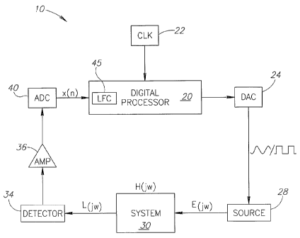
[0029] Fig. I is a schematic diagram of an apparatus that measures
phase shift and amplitude of a system;
[0030] Fig. 2A is a block diagram of the linear filter component of the
digital processor that performs a modified Goertzel Algorithm;
[0031] Fig. 2B is a diagram of a flow graph for an HR filter, in the
digital processor of the apparatus of Fig 1;
8b
CA 02629296 2008-05-09
WO 2007/058978 PCT/US2006/043868
[0032] Fig. 3 is a diagram of excitation and emission two waveforms
associated with the apparatus of Fig. 1;
[0033] Fig. 4A is a diagram of inputs and outputs of the system of the
system of Fig. 1 with sine wave input;
[0034] Fig. 4B is a diagram of an output signal of the modified Goertzel
filter of Fig. 2B that filters the output from Fig. 4A;
[0035] Fig. 5A is a diagram of inputs and outputs of the system of Fig. 1,
with square wave input;
[0036] Fig. 5B is a diagram of an output signal of the modified Goertzel
Filter of Fig. 2B that filters output from Fig. 5A;
[0037] Fig. 6 is a diagram of another embodiment of phase and amplitude
measurement device;
[0038] Fig. 7 is a diagram of another embodiment of a phase and
amplitude measurement apparatus;
[0039] Fig. 8 is a diagram of another embodiment of a phase and
amplitude measurement apparatus that performs down conversion; and,
[0040] Fig. 9 is a diagram of another embodiment of phase and amplitude
measurement apparatus for a luminescent probe that performs down conversion.
DETAILED DESCRIPTION
[0041] The subject matter disclosed herein is directed to apparatus and
methods that utilize linear filters, such as second order linear filters, in
apparatus for
system identification. The linear filters are portions of components, that
utilize
modified Goertzel Algorithms to determine, for example, the phase shift in a
luminescent sample or other system, typically a linear or physical system. The
disclosed subject matter, with its use of linear filters, is highly efficient
in computing
phase or amplitude based on measurements of excitation light and emitted light
from
a luminescent sample or phase and amplitude of input and output electrical
signals of
an impedance network.
[0042] Attention is now directed to Fig. 1, that shows the disclosed subject
matter as an apparatus (system or device) 10 including a digital processor 20,
coupled
with a system 30, for example, a linear or physical system. The digital
processor 20
9
CA 02629296 2008-05-09
WO 2007/058978 PCT/US2006/043868
includes one or more processors, control logic, components, and the like for
determining quantities and measurements, such as the phase, amplitude as well
as
other measurements of the system 30, as well as other quantities or
measurements
such as the phase shift or amplitude ratio between the input signal to the
digital
processor 20 and an output signal, typically output from the digital processor
20.
[0043] The apparatus 10 includes a crystal clock oscillator (CLK) 22, that,
for example, runs at 1 to 25 MHz. The digital processor 20 uses the crystal
clock
oscillator 22 to generate a highly stable periodic signal called the "sample
clock",
typically at frequencies of 200 kHz or less. The sample clock signal is used
to
synchronize the calculation of successive numerical values of an excitation
signal,
such as in the form of sinusoidal waves or square waves. These signals,
represented
by either the sinusoidal wave or the square wave, are synchronously
transferred to a
digital to analog converter (DAC) 24, which transforms the samples to an
electrical
waveform that drives a source 28.
[0044] The source 28 is, for example, a transducer that receives electrical
signals (typically as waves or waveforms) from the DAC 24, and converts it
into
corresponding modulated excitation light or energy, depending on the specific
system
30. For example, when the system 30 includes a luminescent probe molecule or
other
luminescent material, the source 28 typically includes one or more light
emitting
diodes (LEDs). Alternately, when the system 30 includes a sample with
electrical
impedance characteristics, the source emits electric energy (signals) from an
electrode, Radio Frequency (RF) energy from an antenna, or magnetic energy
(signals) from an inductance coil.
[0045] The emitted energy or light from the system 30, is received by a
detector 34, that typically includes a transducer. The transducer includes a
receiver,
such as a photodiode(s) for receiving light, an electrode, for electricity, an
antenna,
for radio frequency, or a coil, for magnetic energy, coupled with a converter,
that
converts the received light or energy (electric, radio frequency or magnetic)
to an
output, typically electrical signals. These electrical signals may be
amplified by an
amplifier (AMP) 36, prior to being received by an analog to digital converter
(ADC)
40. The process of conversion of the electrical signal to digital data in the
ADC 40 is
synchronized to the crystal clock oscillator 22.
CA 02629296 2008-05-09
WO 2007/058978 PCT/US2006/043868
[0046] The ADC 40 sends digital data to the digital processor 20. This
digital data (typically in signals corresponding to waves or waveforms) is
input into
the linear filter component (LFC) 45, formed of a filter 46 and control logic
(CL) 48
(e.g., one or more processors), as shown in Fig. 2A. The filter 46 is, for
example, a
linear filter, such as a second order filter (e.g., a second order digital
filter or second
order digital resonator), and, for example, an Infinite Impulse Response (IIR)
filter
46a. The IIR filter, is, for example, a modified Goertzel filter, as shown in
Fig. 2B.
[0047] The output from the linear filter component 45 is used to determine
the phase shift, expressed as AO, between the input waveform (50 of Fig. 3) to
the
system 30 and the output waveform (55 of Fig. 3) of the system 30, as
described
below. In Fig. 3, the points of sampling on the input waveform 50 and the
output
waveform 55 occur at integral sample number intervals. The process described
below not only measures the phase shift of the system 30, expressed as A0, but
also of
the phase shift contributions of the DAC 24, Source 28, detector 34, amplifier
36,
ADC 40 and any digitally induced phase delays from the Digital Processor 20.
[0048] Should it be desired to determine the phase shift of the system 30,
separate from the phase shift contributions of the components, the phase shift
of the
system 10, expressed as AO, is measured using a system 30 of known phase
shift,
expressed as o, and the measured phase 0, from the system 30. Subsequent
measurements of phase 0 then are corrected with the stored value(s) to obtain
only the
phase shift due to the system 30.
Phase and Amplitude Determination
[0049] The processing of the signal(s) by the linear filter component 45 in
the Digital Processor 20 (or peripheral thereto) are now detailed. The system
30 for
which this signal processing is described, for example, is a luminescent
probe,
although R/C, Radio Frequency and magnetic systems, as detailed above, are
also
suitable, with modifications made to the apparatus 10, to accommodate the type
of
system 30, being well known to those skilled in the art. The second order
digital filter
receives an input signal(s) (in the apparatus 10 from the ADC 40) and produces
an
output signal(s), that is used to calculate the phase shift and amplitude
ratio of the
luminescent probe.
11
CA 02629296 2008-05-09
WO 2007/058978 PCT/US2006/043868
[0050] The second order linear filter, is typically an infinite impulse
response (IIR) filter 46a (Fig. 2B). This IIR filter 46a, as shown in Fig 2B,
filters the
received input signal(s), and the filter output is used by control logic (CL)
48 to
compute the amplitude and phase of the input signal to the digital processor
20, in
order to calculate the amplitude ratio and phase shift of the luminescent
probe (linear
system) from which the requisite measurement or quantity is determined.
[0051] With the system 30 being a luminescent probe, the luminescence
can be modeled with a transfer function, expressed as H(jw) describing the
amplitude and phase response of the emission of the luminescent probe in
response to
excitation energy. The general description of the system 30 is expressed in
Equation
1 (Eq. 1) as:
L(jw) = H(jw)E(jw) Eq. 1
where,
E(jw) is the input excitation light wave, and,
L(jw) is the output luminescent emission.
[0052] - The transfer function H(jw) is defined in Equation 2 as:
H(jw) = A(w)L8(w) = R(w)+1I(w) Eq. 2
[0053] The properties of the transfer function H(jw) are expressed in
polar and rectangular coordinates. In the polar representation A(w) is the
amplitude
at frequency w, and 8(w) is the phase shift at frequency w. In rectangular
coordinates
R(w) is the real part and I(w) is the imaginary part, both being functions of
the
frequency. For example, the phase shift at a certain frequency may be related
to
oxygen or other analyte concentration.
[0054] The second order linear filter 46 of Fig 2A, specifically as an IIR
filter 46a, is shown schematically in Fig. 2B, to which attention is also
directed. The
IIR filter 46a operates on N samples sequentially, typically in real time,
where "N"
represents a finite number of samples. Also, in Fig. 2B, the boxes with Z-1
reference a
delay element, here, a delay by one sample point, and the circled "+" is a
summation.
12
CA 02629296 2008-05-09
WO 2007/058978 PCT/US2006/043868
[0055] The output of the IIR filter 46a is used to obtain a phase shift,
expressed as A0, and an amplitude measurement, expressed as AR, on the
luminescent
sample of the system 30, as follows. The digital processor 20 causes the
source 28 to
output an excitation light wave that is modulated at a known frequency, for a
finite
period of time during which the excitation modulation cycles of either a
sinusoid or
square wave are generated. The resulting emissions of the system 30 are
converted
into N samples by the ADC 40, and are processed by the second order filter 46
(e.g.,
the IIR filter 46a) in the digital processor 20. After filtering N samples,
the LED or
other excitation source 28 is turned off and the linear filter operation is
halted.
[0056] A graphical representation of the data from the ADC 40 and the
digital processor 20 is shown in Fig. 4A, for an input sinusoidal wave, and in
Fig. 5A,
for an input square wave, and includes N discrete samples, and k excitation
cycles, in
both Figs. 4A and 5A, five cycles. Each time a sampled data point, x(n), is
received
from the ADC 40, the following computation is made to implement the IIR filter
46a.
This computation is Equation 3 (Eq. 3), that makes reference to Fig. 2B, and
is
expressed as:
v,,(n)_C2v,,(n-1)-vk(n-2)+x(n) Eq. 3
where
v,. (n) = recursive filter output
x(n) = real nth input value
vk (n -1) = delay line element 1 (delayed by 1 sample)
V,, (n - 2) = delay line element 2 (delayed by 2 samples)
C2 = 2 cos 2k
N
N = number of samples per data set; and,
k = number of cycles of the excitation light wave, which is related to the
frequency at
which the excitation light wave is modulated.
[0057] The relationship between k, N , f nod and fsample is k/N = fnod/fsample
,
where fnod is the modulation frequency and fsa,npieis the sample rate.
13
CA 02629296 2008-05-09
WO 2007/058978 PCT/US2006/043868
The initial conditions on the IIR filter 46a are v,. (-1) = v, (-2) = 0.
[0058] Turning also to Fig. 4B and Fig. 5B, there is shown graphically the
output of the IIR filter 46a, expressed as v,; (n), over N samples, for both
sinusoidal
wave excitation (Fig. 4A) and square wave excitation (Fig. 5A). After N
samples are
received and linearly filtered according to Equation 3 (Eq. 3), the real
component
R(w) and the imaginary component J (w) of the transfer function H(jw) of
Equation
2 (Eq. 2) are calculated as Equation 4 and Equation 5, respectively, as
follows:
R(w) = vk (N) - Clvk (N -1) Eq. 4
'(W) = Slvk (N -1) Eq. 5
where the constants of C1, and Si are expressed as:
C, = cos 2 and S, = sin 2;Tk
[0059] The quantities of C1, C2 and Si can be precomputed based on the
known values of N and k. Recalling that k is the number of excitation cycles
per data
set, and N = number of converted samples per data set, it can be seen that the
ratio k
/ N does not change as the time during which the excitation source, or light
source in
the case of a luminescent system, is activated. Instead, it can be written as
f1õ0d /
fsa,,,ple . Thus these coefficients only need to be recalculated when changing
sampling
frequency in the ADC 40, and/or excitation modulation frequency.
[0060] The phase and amplitude of the signal x(n) is computed as follows:
Depending on the signs of R(w) and 1(w) the phase, expressed as 0, is
calculated using one of the following equations of the "6" Series, or
Equations
6.1-6.6, as follows:
where R(w) > 0 and I(w) > 0
0 = arctan(I(w) /R(w)) Eq. 6.1
where R(w) > 0 and I(w) <0
0 = arctan(I(w) /R(w)) Eq. 6.2
where R(w) < 0 and I(w) > 0
0=180+arctan(I(w)/R(w)) Eq. 6.3
where R(w) < 0 and I(w) < 0
14
CA 02629296 2008-05-09
WO 2007/058978 PCT/US2006/043868
0=arctan(I(w)/R(w))-180 Eq. 6.4
where R(w)=0
O= 90 Eq. 6.5
where 1(w) = 0
8=0 Eq. 6.6
[0061] The arctangent (arctan) may be implemented via a look up table,
using a polynomial approximation or by using a software library function
compatible
with the specific Digital Processor 20, as provided by the compiler
manufacturer.
Suitable low power Digital Processors, for implementing the Second Order
Filter
Algorithm (the modified Goertzel Algorithm) in the linear filter component 45,
include, for example, the MSP430F427 or the MSP430F4270 processors, from Texas
Instruments.
[0062] The amplitude, expressed as A(w) , is calculated using the
following equation
A(w) = I(w)2 +R(w)2 Eq. 7
[0063] This Amplitude A(iw) is now expressed as the obtained amplitude
(A1) in accordance with the amplitude "A" above, to continue the exemplary
calculations.
[0064] The obtained phase 0 and amplitude AI are now used to determine
the phase shift A8 and the Amplitude ratio of the luminescent sample AR, to
obtain the
requisite quantity, measurement or the like.
[0065] Phase shift A0 is expressed by the equation:
AO= 8- ~ Eq. 8.1
where, 0 is the measured or obtained phase of the input signal from the ADC 40
to the
processor 20, as detailed above; and,
is the phase of the output from the digital processor 20 that goes to the DAC
24.
[0066] In the apparatus 10 of Fig. 1, the reference phase is zero, such that
= 0, and the phase shift equation (Eq. 8.1) becomes:
AO= 0
where the phase shift is the measured or obtained phase. This phase shift may
then be
compared against known quantities or measurements, to obtain the requisite
value,
CA 02629296 2008-05-09
WO 2007/058978 PCT/US2006/043868
such as the amount of an analyte present in a material. In many cases AO is
sufficiently close to the phase shift through sample 30 to be used without
further
correction.
[0067] Amplitude ratio AR is expressed by the equation:
AR = AI/Ao Eq. 8.2
where, A, is the measured or obtained amplitude of the input signal to the
processor
20, as detailed above; and,
Ao is the amplitude of the output of 20, defined to be 1.
[0068] In the apparatus 10 of Fig. 1, the amplitude of output from 20 is
one, such that Ao = 1, and Equation 8.2 becomes:
AR = Ai,
where the amplitude ratio is the measured or obtained amplitude. This
amplitude ratio
may then be compared against known quantities or measurements, to obtain the
requisite value, such as the amount of an analyte present in a material.
[0069] When certain conditions are met, the IIR filter process can be
further simplified. If the values of k and N are chosen such that the ratio of
k/N equals
'/, the C2 coefficient equals zero. Then the IIR filter equation, Equation 3
above, becomes Equation 3.1, expressed as:
v,e(n)=x(n)-v,,,(n-2) Eq. 3.1
[0070] With Equation 3.1, replacing Equation 3, the processes for
detennining phase 0, and amplitude A, uses Equations 4 - 7, as detailed above.
[0071] In this case, there are not any multiplications needed to implement
the IIR filter. This optimization greatly simplifies the IIR filter
computation.
Multiplications are more time consuming than additions on digital processors
that do
not have a fixed or floating point hardware multiplier. Table 1, immediately
below,
shows the computational complexity of the IIR filter, for M frequency bins,
one
frequency bin at an arbitrary frequency and one frequency bin when the filter
coefficient equals zero, that is when k/N equals 1/4.
16
CA 02629296 2008-05-09
WO 2007/058978 PCT/US2006/043868
TABLE 1
M Frequency Bins One Frequency Bin One Frequency Bin at 1/4
FS
Multiplies Adds Multiplies Adds Multiplies Adds
IIR MN 2MN N 2N 0 N
Table 1. Real-Time computational complexity of IIR Filter
Infinite Impulse Response (IIR) Filters
[00721 The data sequence x(n) is shown in Fig. 4A as a solid line. Fig. 4B
shows the evolution of the second order IIR Filter output quantity viz. This
quantity is
the output of IIR Filter 46 and is used by the control logic 48 to compute
phase and
amplitude. The dynamic range of magnitude of this quantity vi, will determine
the
size and type (fixed or floating point) of the variables needed in the
calculation. In
the present example, the signal waveform submitted to the IIR filter has a
peak value
of 0.705, as shown in Fig. 4A as a solid line. For the given frequency and 200
samples, the maximum amplitude (absolute value) reached by the output of the
IIR
filter, is 411, as shown in Fig. 4B. Digital resonant filters, such as the IIR
filter
employing at least a portion of the modified Goertzel algorithm, with poles on
the unit
circle behave in this manner, where the output grows without bounds.
[00731 Thus there is an increase by a factor of over 400 in the numerical
magnitude at the output of the IIR filter. This increase is linear in number
of samples,
N, and also depends on the ADC, for example ADC 40, sample frequency. The
frequency dependence is more complicated, producing significantly larger
numerical
magnitudes for frequencies close to zero and close to the Nyquist frequency
than for
frequencies close to half the Nyquist frequency. The Nyquist frequency, as
used
throughout this document, is defined to be half of the sample rate. If a fixed
point
processor is used to perform the IIR filter, care must be taken to select a
variable
width that will accommodate the maximum expected filter output, as determined
by
the number of samples N and the ADC sampling frequency, without overflowing.
If a
processor employing floating-point calculations is used instead of fixed-
point, the
growth in the magnitude of vl, becomes trivial, so as to be negligible.
17
CA 02629296 2008-05-09
WO 2007/058978 PCT/US2006/043868
[0074] In the ideal case, the IIR filter will operate on a sampled stream of
data, the length of which set will contain: 1) an exact integral number of
samples, N,
and 2) an exact integral number of excitation signal cycles, k. It is not
necessary that
the number of samples per excitation signal cycle be integral. For instance,
three
signal cycles in 50 samples (or 3,000 cycles in 50,000 samples) produces an
exactly
correct phase measurement, within arithmetic precision, even though there are
16 2/3
samples per excitation signal cycle.
[0075] In the more usual approach, the ADC sampling rate will be
specified in Hertz (Hz) and fixed, while the modulation frequency of the
excitation
source, and the duration over which N samples are converted, (defined as the
excitation source on time, expressed as ton) will be set as needed for
particular
measurement conditions. For example, for the following parameter set:
ADC Sampling frequency, fsampre = 48 kHz
Excitation Modulation frequency, fnod = 10 kHz
Excitation waveform: sinusoidal
Excitation source on time tnõ = 0.01 second
Total Phase shift through luminescent system and device: 23 degrees
[0076] In this example, there will be N = 0.01 * 48,000 = 480 samples
per data set and k = 0.01 * 10,000 = 100 signal cycles per data set. Because
both of
these products are exactly integral, the phase calculated using the output of
the second
order filter result will be exact.
k = fnod N= 10k 480 = 100
sample 48k
With these parameters, the coefficients are: C1 = 0.258819045, Si = -
0.9659258262,
C2=0.5176380902. After the IIR filter has been propagated, the last two
calculations are shown below, to illustrate the final computation of phase
(0), as:
Real = 195.794103147847 - C1* (-97.083511264731) = 220.921164818631
Imag = Si* (-97.083511264731) = 93.7754708287823
where,
18
CA 02629296 2008-05-09
WO 2007/058978 PCT/US2006/043868
8 = arctan 93.775470828 :k 180 = 23
220.92116481 Tr
[0077] The phase shift (A0, as detailed above), is the difference of the
measured phase of the input signal from the ADC to processor 20 (expressed as
0) and
the phase (~) of the output signal of processor 20, as detailed above in
Equation 8.1,
and provides a value used to characterize the luminescent system's response at
10
KHz. Excitation modulation frequency and phase shift may be used to calculate
a
luminescent lifetime, or phase shift, related to analyte concentration.
[0078] Attention is now directed to Fig. 6, where there is shown an
apparatus 110, that uses linear filters of the disclosed subject matter to
make
differential phase measurements for compensation of unwanted phase delay.
[0079] In this apparatus 110, as well as the apparatus 210, 310 and 410
detailed below, identical or similar components, that have been previously
discussed
above for the apparatus 10 of Fig. 1, will be identified with the same
numerals,
increased by "100" in each succeeding apparatus. These elements, with numerals
increased by "100" for each succeeding apparatus, take the descriptions of the
elements, whose numbering was increased by "100." Additional description is
provided where necessary, and additional elements are described where
necessary, for
understanding of the disclosed subject matter.
[0080] The apparatus 110 includes a digital processor 120. A linear filter
component (LFC) 145, similar to the linear filter component 45 detailed above,
is
implemented in the digital processor 120 (it may also be peripheral thereto).
The
digital processor 120 is in communication with a digital to analog converter
(DAC)
124, that functions to convert digital to analog signals. The DAC 124 drives a
source
128, for example, a light emitting diode (LED), that typically emits blue
light, as the
excitation light. The system 130, for example, includes a luminescent or
fluorescent
probe 130a, on which the excitation light is transferred from the source 128.
[0081] A first photodiode 133, that also forms part of a detector, the
detector also being a transducer, is used to monitor the excitation light
emitted
directly from the source 128. A detector 134, that includes a photodiode 134a
(second
photodiode), the detector 134 also including a transducer, serves to detect
the
luminescent light emitted from the luminescent sample 130a.
19
CA 02629296 2008-05-09
WO 2007/058978 PCT/US2006/043868
[0082] The output from the first photodiode 133 and the second
photodiode 134a, is typically converted into signals by the respective
transducers, is
supplied to an`analog to digital converter (ADC) 140, at the respective inputs
140a,
140b. Each of the inputs 140a, 140b defines a channel 140a, 140b'. The ADC
140,
for example, is a Sigma-delta converter, such as those intended for stereo
sound, as
they are well suited to this application because phase delay offset
(difference, skew)
between the input channels is carefully controlled and minimized through
symmetrical design..
[0083] In this method, the two inputs 140a, 140b to the ADC 140 will be
sampled contemporaneously, typically simultaneously, and the converted data is
supplied to the digital processor 120 as pairs of numbers. In the digital
processor 120,
in the linear filter component 145, two implementations of the second order
filter
algorithm (modified Goertzel Algorithm) are made in series, as described for
the IIR
filter 46a above. Should there be two linear filter components 145, one for
each
channel 140a', 140b', implementations of the second order filter algorithm
(modified
Goertzel Algorithm) are made in parallel.
[0084] As the system 130 is a luminescent probe 130a, the phase shift and
amplitude change (expresses as the amplitude ratio AR), through the probe are
modeled by Equations 1 and 2, as detailed above. The IIR filters, in
accordance with
the IIR filter 46a of Fig 2B, detailed above, are executed in parallel with
separate
delay lines, to accommodate the two separate inputted waveforms. After N
samples
are received over k excitation cycles and linearly filtered according to
Equation 3 (Eq.
3), the real component R(w) and the imaginary component 1(w) of the transfer
function H(jw) of Equation 2 (Eq. 2) are calculated as Equation 4 and Equation
5, as
detailed above, to determine the requisite phase (Oa and Ob), finally
calculated with the
"6" series equations. For both wavefonns, Equation 8.1 for phase shift, as
detailed
above (AOa = 0a - 4 and AOb = Ob - 0 is now applied, and for both waveforms, ~
= 0,
such that Ma = 0, and AOb = 0b. As long as both IIR filters can be executed in
the
time between samples from the ADC 140, each of these will contain all the
phase
shifts contributed by the analog, digital components, and the luminescent
sample of
the system 130.
CA 02629296 2008-05-09
WO 2007/058978 PCT/US2006/043868
[0085] Accordingly, two values for phase are obtained, one for each of the
waveforms, expressed as 0a , from input 140a for the system 130, and 0b, from
input
140b. When the phase of input 140b (0b) is subtracted from the phase of the
input
140a (0a), the difference will be only the sample luminescence phase shift
(AO),
uncontaminated by system delays, either analog or digital.
[0086] The phase shift (AO = 0a - Ob), as detailed above, provides a value
used to characterize the luminescent system's response, and is used, for
example, to
calculate a luminescent lifetime, or related to analyte concentration.
[0087] In the apparatus 110, the only uncompensated phase error between
the channels (which contributes directly to the phase estimate of the sample
in the
system 130) will be due to any difference in delay between the two photodiode-
plus-
preamplifier channels. The more similar these channels are made, the more
exactly
the calculated phase difference will represent delay due to luminescence
lifetime
alone. In practical systems, a procedure can be provided for measuring and
subsequently subtracting any residual phase delay due to mismatch between the
channels. This method is so effective that it is often sufficient merely to
create a
signal path from the output of the DAC 124 to the second input 140b of the ADC
140
that contains an amplifier (not shown). The amplifier roughly duplicates the
phase
shift of the photodiode preamplifier. As a result, residual asymmetry can be
calibrated out. Exactness of measurement then becomes a function of the
stability of
the inter-channel difference, a second-order error.
[0088] However it is arranged, the advantages of the symmetrical dual-
channel system are so great that this approach is strongly recommended in all
cases,
even in the absence of a second photodiode-plus-preamplifier sub-system. It
should
be noted that program delays and phase-offsets in the calculations will also
cancel, as
long as they are present in both channels and all calculations needed for
input samples
can be completed in the time between samples.
[0089] Practical systems will unavoidably have phase delays in the analog
components, and possibly much larger delays in the data converters: the ADC
and
DAC. For this and other reasons, it is advisable to regard all phase
measurement and
calculation as determination of relative phase rather than absolute phase.
That is, it is
generally advantageous for the final result to be the difference between two
measured
21
CA 02629296 2008-05-09
WO 2007/058978 PCT/US2006/043868
phases, whether these measurements are made simultaneously or sequentially. If
sigma-delta converters are used, as they commonly are, data converter phase
delay
can be hundreds of degrees for modulation frequencies near the Nyquist
frequency
limit. Because such phase delay is typically determined by the crystal-
controlled .
system clock, data converter delay is of a digital nature and usually quite
stable. In
these circumstances it may be possible to eliminate it through programming,
but it is
far simpler and more general to remove delays through some form of symmetrical
dual-charnel approach.
Apparatus for Phase Correction
[0090] Fig. 7 shows an apparatus 210 that uses second order filters of the
disclosed subject matter, and makes differential phase measurements, for
compensation of unwanted phase delays. The apparatus 210 includes a digital
processor 220, for example, a microcontroller, the digital processor 220
implementing a linear filter component 245, similar to the linear filter
components 45
and 145 detailed above. The digital processor 220 is electrically coupled to a
crystal
oscillator clock (CLK) 222. The digital processor 220 typically includes an on-
chip
pulse width modulator (PWM) 223, that, for example, outputs a 50% duty cycle
square wave to a driver 228a, the square wave modulating the driver 228a, that
in turn
modulates one of two selectable LEDs 228b, 228c (by a switch 228d, controlled
by a
general purpose input/output (GIPO) 223a) at a fixed frequency. The driver
228a,
selectable LEDs 228b, 228c and switch 228d, define a source 228 (as shown in
the
broken line box), similar to the sources 28, 128, detailed above.
[0091] The driver 228a changes a voltage source waveform, for example,
a square wave, into a current source waveform used for exciting the LEDs 228b,
228c. The excitation LED 228b has a short wavelength spectral output, such as
an
ultraviolet (UV), blue or green LED, that is used to excite a luminescent
sample 230a,
defining the requisite system 230.
[0092] An optical filter 229 is used to improve the spectral purity of the
LED 228b, and eliminate wavelengths of light that overlap the emission
spectrum of
the luminescent sample 230. The choice of the excitation LED 228b is dependent
on
the absorption peak of the luminescent sample 230a of the system 230, and is
known
22
CA 02629296 2008-05-09
WO 2007/058978 PCT/US2006/043868
to those of skill in the art. An optical filter 231 is placed in front of the
detector 234
to block light from the first or excitation LED 228b.
[0093] The second LED 228c is a reference LED. It has a spectral output
of longer wavelengths, such that it does not substantially excite emission
luminescence in the sample 230a. Instead the reference LED 228c feeds directly
through the system 230 or is scattered before it impinges on the detector 234
(the
detector 234, for example, a photodiode, such as a P intrinsic N (PIN)
photodiode). As
a result, the light from the second or reference LED 228c provides a reference
phase
measurement to cancel out unwanted phases of the components of the apparatus
210.
[0094] The reference LED 228c is time-division-multiplexed with the
excitation LED 228b. This reference phase measurement removes phase shifts due
to
the photodiode (of the detector 234), amplifier 236, low-pass filter (LPF) 239
and
sampling process. The spectral output of the reference LED 228c is not
critical,
except that it overlaps (at least partially) the emission of the luminescent
sample 230a
and is detectable by the detector 234.
[0095] A preamplifier 236 amplifies the electrical signal from the
photodiode of the detector 234 (the detector 234 also includes a transducer
like the
detectors 34 and 134 described above, that converts the detected emissions to
electrical signals or the like), and passes it to a low pass filter 239. The
low pass filter
(LPF) 239 removes high frequency components to prevent aliasing in the ADC
240.
For example, the microcontroller has a sigma-delta ADC 240, which samples the
input signal synchronous with the operation of the PWM 223. This is easily
achieved
because the same clock, for example, the crystal oscillator 222, provided to
the
apparatus 210 is used to clock the ADC 240 and the PWM 223. This is
particularly
useful if the reference LED 228c is not used, the PWM modulation waveform
remains
phase locked to the ADC 240. The accuracy of the crystal oscillator clock 222
is
important in order to prevent excitation frequencies from changing and
translating
into errors in the measured phase. Variations in the excitation frequency even
as
much as 100 Hz can cause measurable changes in the phase. The signal from the
ADC 240 is received in the linear filter component 245, where it is processed,
for
example, to determine phase and/or amplitude, as detailed below.
23
CA 02629296 2008-05-09
WO 2007/058978 PCT/US2006/043868
[0096] As the system 230 is a luminescent probe, the phase shift of the
luminescent sample 230a, represented as AO, is computed by making two phase
measurements, one with the excitation LED 228b, known as the total phase and
expressed as Ototal, and a phase measurement from reference LED 228c, known as
the
reference phase, expressed as 6,.of. Both phase shifts are modeled by
Equations 1 and
2, as detailed above.
[0097] The IIR filters, in accordance with the IIR filter 46a of Fig 2B,
detailed above, are executed in series, based on the LED 228b or 228c, that is
active,
to accommodate the two separate inputted waveforms. After N samples are
received
over k excitation cycles and linearly filtered according to Equation 3 (Eq.
3), the real
component R(w) and the imaginary component I(w) of the transfer function H(jw)
of Equation 2 (Eq. 2) are calculated as Equation 4 and Equation 5, as detailed
above,
to determine the requisite phases (Ototal and Oref), each phase, Ototal and
Oref, calculated
with the "6" series equations. For both waveforms, Equation 8.1, as detailed
above, is
now applied, and for both pairs of waveforms, 4 in each waveform pair, is an
unknown value, not equal to zero, but is the same for both waveforms.
Accordingly,
Equation 8.1 for each waveform pair, is expressed as:
AOtotal = Ototal - Eq. 8.1.1
AOref = Oref - Eq. 8.1.2
[0098] The equation to determine the phase shift for the system 230 is
expressed as Equation 9.1, as:
AO = AOtotal - A01-e,ef Eq. 9.1
whereby the phase shift for the system 230 (AO) is expressed as, Equation 9.2,
as:
AO = Ototal - 0ref Eq. 9.2
as the ~ components for each waveform pair cancel each other.
[0099] As long as the IIR filters can execute in the time between samples
from the ADC 140, each of these will contain all the phase shifts contributed
by the
analog, digital components, and the luminescent sample of the system 230. The
difference in the phase shifts will be only the sample luminescence phase
shift (AO),
uncontaminated by system delays, either analog or digital.
24
CA 02629296 2008-05-09
WO 2007/058978 PCT/US2006/043868
[0100] The phase shift (AO = 8total - 8ref), as detailed above, provides a
value used to characterize the luminescent system's response, and is used, for
example, to calculate a luminescent lifetime, or related to analyte
concentration.
[0101] An exemplary operation of the digital processor 220 is now
described, with the following parameters that allow for an excitation
frequency of
5208.333Hz. The requisite parameters are as follows:
Crystal Oscillator Frequency: 8 MHz
ADC Sample Rate (FS): 31.250 kHz
Total Samples (N): 1002
Frequency Index (k): 167
Excitation Frequency (finod): 167/1002*Fs = 5208.333 Hz
Second Order Filter Coefficient: C, = 2 cos(-) = 2 cos(3) =1
[0102] Second Order Filter:
V167(n)=V167(n-1)-v167(n-2)+x(32)
[0103] With this ratio of k/N = 1/6, the real-time Second Order Filter
Coefficient is equal to one. This filter thus requires two additions and no
multiplications.
[0104] In some systems, if the modulation frequencies are sufficiently
low, for example, 1 KHz to 20 KHz, the reference phase (Oref) is negligibly
small or
does not change with time or temperature. In this case the system 210 is
operable
without the reference LED 228c, provided the output from the PWM 223 can be
synchronized with the ADC 240 and the digital processor 220.
[0105] The systems 110 and 210 detailed above, samples, such that the
Nyquist criterion will dictate the minimum acceptable sampling rate, typically
10 or
20 percent higher than twice the highest modulation frequency of the
excitation
source, for example, the respective sources 128, 228. This requirement applies
equally to the rate of signal generation and the digitizing rate of the data
converters,
for example ADCs 140, 240.
[0106] The previously described apparatus 110, 210 use an excitation
waveform that has a fundamental frequency, that is less than the Nyquist
frequency of
CA 02629296 2008-05-09
WO 2007/058978 PCT/US2006/043868
the analog-to-digital converter (ADC) 140, 240. This restricts the apparatus
110, 210
to low excitation frequencies, as higher excitation frequencies require the
use of
expensive high-speed ADCs. Additionally, the high speed ADCs typically do not
have the same bit resolution as the lower speed ADCs.
Apparatus for Down Conversion
[0107] The disclosed subject matter provides apparatus that allow the
fundamental of the excitation frequency to be greater than the Nyquist
frequency of
the ADCs. These apparatus are shown in Figs. 8 and 9, and employ processes
known
as down conversion, and supporting structure.
[0108] Figure 8 shows an apparatus 310, that implements the
aforementioned down-conversion process. The apparatus 310 includes a digital
processor 320 with linear filter components 345a, 345b, that implement the
second
order linear filter algorithm (a modified Goertzel Algorithm), as described
above, for
the digital processor 20 of Fig. 1. The apparatus 310 employs mixers 338a,
338b,
typically mixers that implement analog mixing functions, such as diode
bridges,
analog multipliers and Gilbert Cells. These mixers 338a and 338b, perform the
down
converting functions, detailed below.
[0109] A first mixer 338a, receives output from the system 330, via the
detector 334 (the detector 334 also includes a transducer like the detectors
34, 134 and
234 described above, that converts the detected emissions, signals or the
like, to
electrical signals or the like), and amplifier 336, as well as output from a
second
digital to analog converter (DAC) 324b. This second DAC 324b, for example, may
be a one-bit pulse width modulator, to produce a square wave, or a high speed,
for
example, 0 Hz to 1 GHz Direct Digital Synthesis (DDS) component. A second
mixer
338b receives output from the source 328 (the source 328 may be any of the
sources
detailed for the source 28 of Fig. 1 above, with a light emitting diode being
typical),
as well as output from a second digital to analog converter (DAC) 324b, as
detailed
immediately below.
[0110] The apparatus 310 performs a method, where the digital processor
320, generates a waveform at first frequency (fl), having phase of 41 and
amplitude of
Al, for digital to analog converter (DAC) 324a, on a first channel, and a
waveform at
26
CA 02629296 2008-05-09
WO 2007/058978 PCT/US2006/043868
second frequency (f2), having phase of 4)2 and amplitude of A2, for a second
DAC
324b. This first DAC 324a, for example, may be a one-bit pulse width
modulator, to
produce a square wave, or a high-speed, for example, 0 Hz to 1 GHz, Direct
Digital
Synthesis (DDS) component. This second waveform at frequency (f2) is used to
mix
(multiply) both the output waveform of the system 330 and the input waveform
to the
system 330. The system 330 may be any of the systems detailed above for the
system
30 of Fig. 1. A luminescent system is typical as the system 330.
[0111] The result of this process is that a sum frequency, fl+f2, and
difference frequency, fl-f2, are generated at the output of mixers 338a and
338b. The
second frequency (f2) is chosen so that the difference between the first
excitation
frequency (fl) and the second mixer frequency (f2), fl-f2 is less than the
Nyquist
frequency of the ADCs. This requirement allows the ADC 340a, 340b to sample
the
waveforms without aliasing. The sum frequency is usually much greater than the
Nyquist frequency so it is easy to filter out using a low pass filter (LPF)
339a, 339b,
for each of the channels. This apparatus 310 is particularly useful, in that
the down-
converted difference frequency from mixer 338a still retains the phase and
amplitude
information of the original higher frequency output waveform as explained
below.
Thus the phase shift, A0, and amplitude As through the System 330, detector
334 and
amplifier 336 at an excitation modulation frequency of f1, can be preserved
and
transferred to the lower frequency fl-f2.
[0112] For sinusoidal waveforms, the mixing process in the mixer 338b
can be written as follows:
x, (t) = As A, sin(2,7f,t+0, + AB) Eq. 10
x2 (t) = A, sin(2TCf, t + 0,) Eq. 11
m(t) = A2 sin(2TCft + O,) Eq. 12
Y, (t) = x, (t) * m(t) Eq. 13
y2 (t) = x2 (t) * m(t) Eq. 14
and,
27
CA 02629296 2008-05-09
WO 2007/058978 PCT/US2006/043868
y,(t)=As Al 2 cos(2jT(f -f2)+02 -01 A O ) f, +f2)+02 +01 +A&)
Eq. 15
y2(t)= A,A2 cos(2,7(f -f2)+Y'2 -7"])+ 111A2 cos(2/T(f +f2)+7'2 +0,)
1 Eq. 16
where,
f , Al are excitation waveform frequency, phase and amplitude
respectively;
f2 , ~2, A2 are mixing waveform frequency, phase and amplitude respectively;
AS , is the amplitude of the system;
A8, is the phase shift caused by the system;
X, (t), is the input to the mixer 338a, comprising output of system 330,
having
phase A0+41 and amplitude AIAs;
x2 (t) , is the input to the mixer 33 8b, comprising the excitation waveform,
having phase 41 and amplitude A1;
in (t) , is the mixing waveform input to the mixers 338a and 338b;
y, (t) , is the output waveform of the mixer 338a; and,
y2 (t) , is the output waveform of the mixer 338b.
[0113] The multiplication of the two sine waves of different frequencies
generate two other sine waves, one of which is at the difference frequency and
the
other at the sum frequency, as shown by Eqs. 10, 12, 13 and 15 for the mixer
338a,
and Eqs. 11, 12, 14 and 16 for the mixer 338b. The other significant result is
that the
phase information of both the excitation waveform and the mixing waveform is
retained in the mixing process. According to the equations above for the mixer
338a,
the output of the mixer 338a is a waveform at sum, fl+f2, and difference, fl-
f2,
frequencies. The output of the mixer 338a is filtered by LPF 339a, resulting
in a
waveform with a difference in frequencies f1-f2, and according to Equation 15
above,
there is a phase Oa = L\0 + ((p1-42), and an amplitude Aa = A1A2As/2,
[0114] Correspondingly the result of mixing in 33 8b is similarly
explained. According to the equations 11, 12, 14 and 16 above for mixer 338b,
the
28
CA 02629296 2008-05-09
WO 2007/058978 PCT/US2006/043868
output of 338b is a waveform with sum, fl+f2, and difference, fl- f2,
frequencies. The
output of mixer 338b is filtered by LPF 339b, resulting in a waveform with a
difference in frequencies f1-f2, and according to Equation 16 above, there is
a phase Ob
_ (~i-+2), and an amplitude Ab = A1A2/2.
[0115] Since the mixing waveform is used in both mixers 338a, 338b to
mix the output of the system 330 as well as the input to the system 330, the
phase ~2
of the mixing waveform can be removed by computing a phase difference, Oa-0b,
in
the digital processor 320.
[0116] The phase shift of the system 330, detector 334 and amplifier 336,
represented as AO, is computed by making two phase measurements, one from the
output of ADC 340a, known as the total phase and expressed as Ototal= AO + (~1-
~2),
shown as Oa output from LFC 345a , and a phase measurement from the other ADC
340b, known as the reference phase, expressed as O,-ef= (4'i+), shown as Ob
output
from LFC 345b.. The IIR filters, in accordance with the IIR filter 46a of Fig
2B,
detailed above, are executed in parallel, as the output from each ADC 340a,
340b is
inputted to corresponding linear filter components 345a, 345b in the digital
processor
320. In each of the linear filter components 345a, 345b, after N samples are
received
over k excitation cycles and linearly filtered according to Equation 3 (Eq.
3), the real
component R(w) and the imaginary component 1(w) of the transfer function H(jw)
of Equation 2 (Eq. 2) are calculated as Equation 4 and Equation 5, as detailed
above,
to determine the requisite phases (Ototat and 01.ef), each phase, 0totat and
Oref, calculated
with the "6" series equations.
[0117] The equation to determine the phase shift AO of the system 330,
detector 334, and amplifier 336 is expressed as, Equation 9.2, as:
AO = Ototal - Oref Eq. 9.2
as explained above the (~1-42) components for each waveform pair cancel each
other.
[0118] As long as the IIR filters can execute in the time between samples
from the ADC 140, each of these will contain all the phase shifts contributed
by the
analog, digital components, and the luminescent sample of the system 330. The
difference in the phase shifts will be only the phase shift due to system 330,
detector
29
CA 02629296 2008-05-09
WO 2007/058978 PCT/US2006/043868
334 and amplifier 336, but uncontaminated by other system delays, either
analog or
digital
[0119] The phase shift (DO = Ototal - O,.ef), as detailed above, provides a
value used to characterize the luminescent system's response, and is used, for
example, to calculate a luminescent lifetime, or related to analyte
concentration.
[0120] The amplitude ratio of the system 330, represented as As, is
computed by making two amplitude ratio measurements, one from the output of
ADC
340a, known as the total amplitude, and expressed as Atotai , and an amplitude
from the
other ADC 340b, known as the reference amplitude, expressed as Aref. Both
amplitude ratios are modeled by Equations 15 and 16, as detailed above. The
IIR
filters, in accordance with the IIR filter 46a of Fig 2B, detailed above, are
executed in
parallel, as the output from each ADC 340a, 340b is inputted to corresponding
linear
filter components (LFC) 345a, 345b in the digital processor 320. In each of
the linear
filter components 345a, 345b, after N samples are received over k excitation
cycles
and linearly filtered according to Equation 3 (Eq. 3), the real component R(w)
and the
imaginary component 1(w) of the transfer function H(jw) of Equation 2 (Eq. 2)
are
calculated as Equation 4 and Equation 5, as detailed above, with the requisite
amplitudes obtained (Atotai and Aref) calculated with Equation 7. For both
pairs of
waveforms, a ratio according to Equation 8.2, as detailed above, is now
applied, and
for both pairs of waveforms, AIA2/2 in each waveform pair, is an unknown
value, not
equal to zero or 1. Accordingly, Equation 8.2 for each waveform pair, is
expressed
as:
Atotal = AIA2A5/2 Eq. 8.2.1
Aref =A I A2/2 Eq. 8.2.2
[0121] The equation to determine Amplitude for the system 330 (As) is
expressed as, Equation 17, as:
As = Atotal / Aref Eq. 17
as the AI and A2 components for each waveform pair cancel each other.
[0122] Fig. 9 shows an apparatus 410, that uses a digital processor 420,
with linear filter components (LFC) 445a, 445b. The digital processor 420
includes a
micro controller. The apparatus 410 operates in a down-converting mode (by
virtue of
using a mixer 438). The down-converting mode extends the range of excitation
CA 02629296 2008-05-09
WO 2007/058978 PCT/US2006/043868
modulation frequencies to measure shorter luminescent lifetimes. Without the
down-
conversion, the highest modulation frequency for this system 430 would be
about 16
KHz because the sample rate is 31.25 KHz. With down-converting the highest
modulation frequency could be as high as 250 KHz.
[0123] For example, the apparatus 410 of Fig. 9 may use an excitation
modulation frequency, f1, of about 123 KHz. The requisite parameters are as
follows:
Crystal Oscillator Frequency (CLK): 8 MHz
ADC Sample Rate (Fs): 31.250 kHz
Crystal to ADC ratio (R): 256
PWM Mixer Frequency (f2): 8MHz! 64 = 125.0000 kHz
PWM Excitation Frequency (fl): 8MHz/ 65 = 123.0769 kHz
Crystal to Mod. Frequency Ratio (M): M=65
Difference Frequency f2-f1(fdiff): f2 - fl = 1923.076923 Hz
Sum Frequency f2+f1 (fSll1õ ): f2 + fl = 248076.9230 Hz
Total Samples (N): N = M*17 = 1105
Frequency Index (k): k R M M N=68
Second Order filter coefficient:
C2 = 2 cos(- ) = 2 cos(2;r68) =1.852349 Eq. 18.1
N 1105
Second Order filter:
V68 (n) = C, v68 (n -1) - V68 (n - 2) + x(n) Eq. 18.2
[0124] By choosing the window length (N) to be a whole number multiple
of the crystal to modulation frequency ratio (M) this gives a whole number
value for
the frequency index k. Equation 18.1 shows the Second Order filter coefficient
for
the given values for k and N. The sum frequency is shown above to illustrate
that this
frequency is well outside of the bandwidth of the ADCs 440a, 440b and is
easily
attenuated by each low-pass filter (LPF) 439a, 439b, before it is sampled by
the ADC
440a, 440b.
31
CA 02629296 2008-05-09
WO 2007/058978 PCT/US2006/043868
[0125] - The apparatus 410 includes a microcontroller with two ADCs 440a,
440b, typically internal thereto, that send their respective output, x1(n) and
x2(n),
(signals) to the respective linear filter components 445a, 445b, that are
implemented
by the microcontroller (of the digital processor 420).
[0126] The apparatus 410 also includes two pulse width modulators
(PWM) 423a (PWM1) and 423b (PWM2), that generate a square wave excitation
signal at frequency-fl and a square wave mixing signal at frequency f2. The
two pulse
width modulators (PWM1, PWM2) 423a, 423b may also be direct digital synthesis
(DDS) engines that generate sign wave functions, and the apparatus 410 would
operate similar to the operation detailed below.
[0127] The square wave output of PWM1 423a drives a source 428,
comprising a driver 428a that modulates an excitation (EXC.) LED 428b at
frequency
fl. The square wave output of PWM1 423a also connects to differential
amplifier
438b. The excitation LED 428b directs excitation light to the system 430, for
example, a luminescent sample or probe 430a, typically through an excitation
filter
429.
[0128] The square wave output of PWM2 423b connects to the switch
component 438c or multiplexing switch of mixer 438, and causes the switch
component 438c to actuate at frequency f2. There is an analog mixer 438,
formed of
differential amplifiers (D. Amp) 438a, 43 8b coupled to the switch component
438c,
that includes a single-pole-double-throw (SPDT) switch, formed of two switches
438c' and 438c". Each switch 438c' and 438c" is coupled with a corresponding
differential amplifier 438a, 438b. The outputs of the differential amplifiers
438a,
43 8b are fed into the input of the switch component 43 8c.
[0129] The emission of luminescent sample or probe 430a, typically
passes through an emission filter 431, and is converted to an electrical
signal by the
detector 434, for example, including a photodiode (e.g., a PIN photodiode) and
a
transducer (as detailed above for detectors 34, 134, 234 and 334), with the
signal
amplified by amplifier 436, and then sent to the differential amplifier 438a.
The
output of 438a is also fed into the inputs of the switch component 438c, in
particular
switch 438c'. The switch 438c' position is controlled by a periodic square
wave at the
mixing frequency, f2, that is supplied by PWM2 423b. This combination
effectively
32
CA 02629296 2008-05-09
WO 2007/058978 PCT/US2006/043868
multiplies the signal by plus and minus one. The apparatus 410, by using SPDT
switches, may have up to as many as four SPDT switches in a single package.
This
allows for four mixers in one small package.
[0130] This combined mixing approach has some advantages. One
advantage is that the mixing frequency has a wide dynamic range with some
components going up to 100 MHz and extending all the way down to DC, for
example, less than 10 Hz. The mixers 338a, 338b can be turned off completely,
by
setting the output of 324b to one state when down-conversion is not required,
such as
when the source modulation frequency, fl, is less than the Nyquist frequency
of the
ADCs 340a, 340b. A second advantage is that this is a linear operation that
will not
cause distortion due to the mixing process.
[0131] In this down-converting apparatus 410, two linear filter
components 445a, 445b are executed contemporaneously, and typically
simultaneously (in parallel), within the sample period of the ADCs 440a, 440b,
to
obtain two phase shifts of the data stream from each channel, expressed as DOa
(whose
input is the output from ADC 440a) and DOb (whose input is the output from ADC
440b), respectively. From these two phase shifts AO,, and AN the phase shift
of the
system 430, expressed as AO, is computed and obtained. The ADC 440a is from
the
system, and defines a system or "total" channel, while the ADC 440b is from a
reference, and defines a "reference" channel.
[0132] The second order IIR filters (in accordance with the IIR filter 46a
shown in Fig. 2B and described above) of linear filter components 445a and
445b
operate in parallel as data streams x1(n) and x2(n) are received. Both phase
shifts (DOa
and 4Ob) are modeled by Equations 1 and 2, as detailed above. The IIR filters
typically execute in parallel, as the output from each ADC 440a, 440b is
inputted to
corresponding linear filter components 445a, 445b in the digital processor
420. In
each of the linear filter components 445a, 445b, after N samples are received
over k
excitation cycles and linearly filtered according to Equation 3 (Eq. 3), the
real
component R(w) and the imaginary component 1(w) of the transfer function H(jw)
of Equation 2 (Eq. 2) are calculated as Equation 4 and Equation 5, as detailed
above,
to determine the requisite phases (Oa and Ob) each phase, Oa and Ob,
calculated with the
"6" series equations.
33
CA 02629296 2008-05-09
WO 2007/058978 PCT/US2006/043868
[0133] Both pairs of waveforms output from the mixer 438, and processed
by the linear filter components 445a, 445b, have phase and amplitude as
predicted by
Equations 6.1-6.6 and 7, detailed above. That is, for each waveform pair,
Equation
8.1 is expressed as:
Oa(total) _ AO + (41-42) Eq. 8.1.1'
Ob(ref) = (41-02) Eq. 8.1.2'
[0134] The computed reference phase for ADC reference channel (from
ADC 440b) is subtracted from the computed signal phase for ADC system or total
channel (from ADC 440a), in accordance with, Equation 9.2, as:
AO = Oa(total) - Ob(ref) Eq. 9.2.1
whereby the phase difference represents the phase shift through the system
430,
detector 434, and amplifier 436.
[0135] The quantity AO, from Equation 9.2.1, may then be used to
calculate an analyte concentration using a theoretical or empirically derived
calibration model, or the time constant (lifetime) of the system 430 can be
calculated
[0136] When the time constant or lifetime of the luminescent sample or
probe 430a is relatively long, the mixer 438 can be turned off by setting the
PWM2
423b output in a fixed state either high or low. In this case a mixing
function is not
performed and the highest modulation is limited to approximately 16 kHz.
[0137] While preferred embodiments of the disclosed subject matter have
been described, so as to enable one of skill in the art to practice the
disclosed subject
matter, the preceding description is intended to be exemplary only. It should
not be
used to limit the scope of the disclosure, which should be determined by
reference to
the following claims.
34