Note: Descriptions are shown in the official language in which they were submitted.
CA 02629767 2010-02-15
WO 2007/076176 PCTIUS2006/060791
SMART BUSTER PACK
SPECIFICATION
BACKGROUND OF THE INVENTION
1. FIELD OF INVENTION
The current invention relates to security tags and more particulary, discloses
a blister pack
that comprises an EAS or RFID coil or antenna as part of the metal layer (eg.,
aluminum) seal and
to which a capacitor strap or chip strap can be electrically coupled to form
the EAS or RFID
security tag.
2. DESCRIPTION OF RELATED ART
Tracking or detecting the presence or removal of retail items from an
inventory or retail
establishment comes under the venue of electronic article surveillance (EAS),
which also now
includes radio frequency identification (RFID). EAS or RFID detection is
typically achieved by
applying an EAS or RFID security tag to the item or its packaging and when
these security tags are
exposed to a predetermined electromagnetic field (e.g., pedestals located at a
retail establishment
exit), they activate to provide some type of alert and/or supply data to a
receiver or other detector.
However, the application of the EAS or RFID security tag to the item or its
packaging in
the first instance can be expensive and wasteful of resources used to form the
security tag. For
example, EAS security tags, typically comprise a resonant circuit that utilize
at least one coil and
at least one capacitor that operate to resonate when exposed to a
predetermined electromagnetic
field (e.g., 8.2 MHz) to which the EAS tag is exposed. By way of example only,
the coil and the
capacitor are etched on a substrate whereby a multi-turn conductive trace
(thereby forming the
coil) terminates in a conductive trace pad which forms one plate of the
capacitor. On the opposite
side of the substrate another conductive trace pad is etched to form the
second capacitor plate,
while an electrical connection is made through the substrate from this second
plate to the other
end of the coil on the first side of the substrate; the non-conductive
substrate then acts as a
dielectric between the two conductive trace pads to form the capacitor. Thus,
a resonant circuit is
formed. Various different resonant tag products are commercially available and
described in
issued patents, for example, U.S. Pat. Nos. 5,172,461; 5,108,822; 4,835,524;
4,658,264; and
CA 02629767 2010-02-15
WO 2007/076176 PCT/US2006/060791
4,567,473 all describe and disclose electrical surveillance tag structures.
However, such products
utilize, and indeed require, substrates which use patterned sides of
conductive material on both
face surfaces of the substrate for proper operation. Special conductive
structures and
manufacturing techniques must be utilized on both substrate faces for
producing such resonant tag
products. Currently available EAS tag structures have numerous drawbacks. For
example, since
special patterning and etching techniques must be utilized on both sides of
the available tags to
produce the proper circuit, per unit processing time and costs are increased.
Furthermore, the
complexity of the manufacturing machinery required for production is also
increased. Oftentimes,
complex photo-etching processes are used to form the circuit structures. As
may be appreciated,
two sided photo-etching is generally time consuming and requires precise
alignment of the
patterns on both sides. Additional material is also necessary to pattern both
sides, thus increasing
the per unit material costs.
With particular regard to radio frequency identification (RFID) tags, RFID
tags include an
integrated circuit (IC) coupled to a resonant circuit as mentioned previously
or coupled to an
antenna (e.g., a dipole) which emits an information signal in response to a
predetermined
electromagnetic field (e.g., 13.56 MHz). Recently, the attachment of the IC
has been
accomplished by electrically-coupling conductive flanges to respective IC
contacts to form a "chip
strap." This chip strap is then electrically coupled to the resonant circuit
or antenna. See for
example U.S. Patent Nos. 6,940,408 (Ferguson, et al.); 6,665,193 (Chung, et
al.); 6,181,287
(Beigel); and 6,100,804 (Brady, et al.).
Applying such EAS or RFID security tags to pharmaceutical blister packs is
challenging
because of the blister pack construction. A typical pharmaceutical blister
pack comprises pills,
tablets, or capsules that are positioned inside a plastic or paper tray which
is then heat sealed with
an aluminum layer. The presence of the aluminum layer can affect EAS or RED
security tag
performance. Thus, there remains a need for more efficiently providing or
integrating a security
tag on or with items and/or their packaging where an aluminum layer is
associated with the item
and/or its packaging.
BRIEF SUMMARY OF THE INVENTION
A blister pack comprising: non-conductive layer comprising a plurality of
compartments
holding respective elements (e.g., pills, tablets, capsules, etc.) and located
substantially within a
central region of the non-conductive layer (e.g., polystyrene) and wherein the
non-conductive
2
CA 02629767 2008-05-14
WO 2007/076176 PCT/US2006/060791
layer further comprises at least one channel running through a margin region
that surrounds the
central region; a metal layer (e.g., aluminum) that is sealed over the central
region for securing the
elements within the plurality of compartments; and a security tag (e.g., an
EAS security tag, an
RFID security tag) positioned within the at least one channel.
A method for integrating a security tag (e.g., an EAS security tag, an RFID
security tag) in
a blister pack having a non-conductive layer (e.g., polystyrene) having a
plurality of compartments
holding respective elements (e.g., pills, tablets, capsules, etc.) therein and
located substantially
within a central region of the non-conductive layer and wherein a metal layer
(e.g., aluminum) is
sealed over the non-conductive layer. The method comprises the steps of:
forming at least one
channel in a margin region surrounding the central region before the metal
layer is sealed over the
non-conductive layer; sealing the metal layer over the non-conductive layer;
severing a portion of
the metal layer that is positioned over the at least one channel; disposing
the severed portion
within the at least one channel; creating a gap in a portion of the severed
portion; and electrically
coupling a capacitor or a radio frequency identification (RFID) integrated
circuit across the gap.
A blister pack comprising: a non-conductive layer (e.g., polystyrene)
comprising a
plurality of compartments holding respective elements (e.g., pills, tablets,
capsules, etc.) and
located substantially within a central region of the non-conductive layer and
wherein the non-
conductive layer comprises a margin region that surrounds the central region;
a metal layer(e.g.,
aluminum) that is sealed over the central region for securing the elements
within the plurality of
compartments; and a security tag (e.g., an EAS security tag, an RFID security
tag) coupled to the
non-conductive layer in the margin region.
A method of producing a blister pack comprising an integrated security tag or
inlay formed
of a metal layer and wherein the blister pack comprises non-conductive layer
having a plurality of
compartments holding respective elements therein and located substantially
within a central region
of the non-conductive layer and defining a margin region surrounding the
central region. The
method comprises the steps of. applying a patterned adhesive to the margin
region of the non-
conductive layer and to the central region, wherein the patterned adhesive
applied in the margin
region has the form of at least one loop having two respective ends; applying
a metal layer to the
non-conductive layer having the patterned adhesive thereon; cutting the metal
layer in the form of
at least one loop having two respective ends to form a coil or antenna in the
margin region;
removing all portions of the metal layer that are not coupled to the non-
conductive layer by any
portion of the patterned adhesive; and coupling a capacitor or a radio
frequency identification
3
CA 02629767 2008-05-14
WO 2007/076176 PCT/US2006/060791
(RFID) integrated circuit across across different portions of said at least
one loop (e.g., the two
respective ends of the at least one loop).
BRIEF DESCRIPTION OF SEVERAL VIEWS OF THE DRAWINGS
The invention will be described in conjunction with the following drawings in
which like
reference numerals designate like elements and wherein:
Fig. 1 is an exploded isometric view of an upper tool and lower tool that
receive a blister
pack therebetween and wherein the upper and lower tool sandwich the blister
pack to form an
EAS or RFID coil or antenna using the metal layer of the blister pack;
Fig. 2 is an isometric view of the smart blister pack of the present invention
showing
continuous concentric slices in the metal layer;
Fig. 2A is an exploded view showing the conductive traces, and removed
portions of
conductive traces or paths, that are positioned within the channels of the
smart blister pack;
Fig. 3 is a cross-sectional view of the blister pack and combined tools (with
the upper tool
being shown in partial cross-section) taken along line 3-3 of Fig. I showing
the upper tool
severing portions of the aluminum seal of the blister pack to form the slices
and recessed coils or
antennas, while applying a vacuum to capture severed portions of the coils or
antennas;
Fig. 4 is a cross-sectional view of the blister pack and the lower tool as the
upper tool,
shown in partial cross-section, has been lifted upward from the lower tool;
Fig. 5 is a cross-sectional view of the blister pack and the lower tool taken
along line 5-5
of Fig. 1 and showing a chip strap being electrically coupled across one of
the gaps in the coil or
antenna;
Fig. 6 is a cross-sectional view of the blister pack and the lower tool taken
along line 6-6
of Fig. 1;
Fig. 7 is a cross-sectional view of an alternative embodiment of the blister
pack and
corresponding tooling (the upper tool being shown in partial cross-section)
just prior to closure of
the tools;
Fig. 8 is a cross-sectional view of the alternative embodiment of the blister
pack depicting
the closure of the corresponding tools and the recessing of the severed
portion to form the gap(s)
in the conductive paths;
Fig. 9 is a cross-sectional view of the alternative embodiment of the blister
pack still in the
lower tool with the upper tool (shown in partial cross-section) being lifted
upward from the lower
tool;
4
CA 02629767 2008-05-14
WO 2007/076176 PCT/US2006/060791
Fig. 10 is a plan view of the conductive traces that form either the coil or
antenna in the
aluminum seal of the blister pack with a capacitor strap being electrically
coupled across a gap in
the coil to forma security tag,
Fig. I OA depicts the equivalent circuit of the circuit formed by the security
tag of Fig.10;
Fig. 11 is a plan view of a pair of concentric coils having respective
capacitor straps
applied respective gaps in the coils to form two security tags;
Fig. 11 A depicts the equivalent circuit of the circuits formed by the
security tags of Fig.
11;
Fig. 12 is a plan view of a pair of concentric dipole antennas having
respective capacitor
straps and an integrated circuit applied respective gaps in the dipole
antennas to form two RFID
security tags;
Fig. 12A depicts the equivalent circuits of the circuits formed by the
security tags of Fig.12;
Fig. 13 which depicts a single EAS coil comprising a plurality of loops; and
Fig. 13A depicts the equivalent circuits of the circuits formed by the
security
tags of Fig. 13.
DETAILED DESCRIPTION OF THE INVENTION
Fig. 2 provides an isometric view of the smart blister pack 20 of the present
invention.
However, before the smart blister pack 20 is discussed in detail, the
construction of a typical
blister pack 10 (see Fig. 1) is discussed. As is well known, the blister pack
10 comprises a non-
conductive layer (e.g., polystyrene) 12 comprising cavities 14 for holding
respective contents 15
(Fig. 6), e.g., pills, tablets, capsules, etc. An aluminum layer 16 is then
heat sealed over the non-
conductive layer 12, thereby sealing the contents 15 therein. To remove one of
the contents 15, a
user need only apply pressure against the particular cavity 14 (Fig. 6)
sufficient to rupture the
aluminum layer 16 directly over the cavity 14 and the contents 15 is then
exposed and ready for
use or ingestion by the user.
The method of the present invention takes advantage of the portion 16A of the
aluminum
layer 16 that surrounds the array of cavities 14. Instead of applying an EAS
or RFID tag to the
blister pack 10, in the present invention the aluminum layer 16 is modified to
contain the EAS or
RFID tag therein. As will be described in detail later, tools are used to
isolate a portion 16A of the
aluminum layer 16 from the remainder of the aluminum layer 16 without
compromising the seal
of the cavities 14. This is accomplished by simultaneously severing an
aluminum layer path along
the outer portion or margin I 6A of the blister pack 10 and then entrenching
this severed path
within the non-conductive layer 12. This path then forms an EAS coil, or an
RFID antenna or
CA 02629767 2008-05-14
WO 2007/076176 PCT/US2006/060791
dipole. It should be noted that more than one EAS coil or RFID antenna or
dipole can be formed
in the margin 16A of the aluminum layer 16, e.g., concentric coils or antennas
or dipoles can be
formed, as shown in Figs. 11-12, by way of example only. Alternatively, an EAS
coil can be
formed in the blister pack 10 that may include a plurality of loops, such as
that shown in Fig. 13.
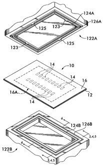
By way of example only, Fig. 1 depicts an exploded view of a tool used for
forming a pair
of security tags within the blister pack 10. In particular, the tool comprises
an upper die 122A and
a lower die 122B. The construction of the dies forms two concentric coils in
the margin 16A of
aluminum layer 16 but again, this is only by way of example. It should be
understood that the term
"margin" is used in its broadest sense and is not limited to the extreme sides
of the blister pack 10;
what is meant by the term "margin" 16A is that portion of the blister pack 10
that does not impact
or disturb the normal operation or seal of the cavities 14.
In particular, where a pair of security tags are desired, the lower die 122B
comprises a pair
of concentric troughs 124B and 126B and the upper die 122A comprises a
corresponding pair of
punches 124A and 126A. The punches 124A and 126A comprise knife edges that
sever
corresponding continuous paths 132 and 134 (see Fig. 2A) of aluminum from the
margin 16A
when the blister pack 10 is sandwiched between the upper and lower dies
122A/122B. It should
also be noted that a plurality of respective projections 123 and 125 are
provided at predetermined
locations along the punches 124A and 126A. The projections 123 and 125,
comprising cutting
edges 133 (Fig. 4), sever respective portions 132P1, 132P2, 134P1 and 134P2
(see Fig. 2A) of the
aluminum paths 132 and 134 created by the punches 124A and 126A, the purpose
of which will
be discussed later.
Also, the non-conductive layer 12 of the blister pack 10 itself comprises a
corresponding
pair of channels therein; one portion of the inner channel 128 is shown in
Figs. 3-4 and one
portion of the outer channel 130 is also shown in Figs. 3-4. Thus, when the
blister pack 10,
having the inner and outer channels 128/130 already formed in the layer 12, is
positioned on the
lower die 122B, the inner and outer channels 128/130 register with the inner
troughs 124B and
126B, as shown in Figs. 3-4. Next, the upper die 122A is then pressed downward
onto the lower
die 122B holding the blister pack 10. When the dies 122A/1 22B sandwich the
blister pack 10, the
punches 124A/I 26A sever the respective aluminum paths 132 and 134 from the
margin 16A and
entrenches them into the corresponding channels 128 and 130. At the same time,
the projections
123 and 125 sever portions 132P 1, 132P2, 134P I and 134P2, that creates
corresponding gaps
132G 1, 132G2, 134G 1 and 134G2 in the corresponding aluminum paths. As can
most easily be
6
CA 02629767 2010-02-15
WO 20071076176 PCT1US2006/060791
seen in Figs. 3-4, each of the projections 123 and 125 comprise lumens 136 and
138 that are
coupled to a vacuum source (not shown). Thus, once the severed portions
I32P1,132P2,134P1
and 134P2 are created, a vacuum is pulled directly against these severed
portions I32P 1,132P2,
134P1 and 134P2 and as the upper die 122A is lifted upward (Fig. 4), the
severed portions 132P1,
I32P2, 134P 1 and 134P2 are removed from the channels 128 and 130, thereby
leaving the gaps
13261, 13202,13401 and 13402 in the conductive paths 132 and 134. Thus, as
shown in Fig. 2,
the result is a pair of continuous concentric slices 137/139 in the margin 16A
of the metal layer
16.
The aluminum paths 132 and 134 positioned inside the channels 128 and 130 form
respective dipoles for an RFID security tag. All that needs to be done is to
electrically couple an
RFID integrated circuit (IC) across one of the two gaps in each of the paths
132 and 134. The
attachment of the RFID IC has been accomplished by electrically-coupling
conductive flanges to
respective IC contacts to fora a "chip strap." This chip strap is then
electrically coupled to the
resonant circuit or antenna. See for example U.S. Patent Nos. 6,940,408
(Ferguson, et al.);
6,665,193 (Chung, et al.); 6,181,287 (Beigel); and 6,100,804 (Brady, et al.).
Fig. 5 depicts a "chip strap" 139
electrically coupled across the gap 132G1 where the RFID IC is shown at 141.
As a result, the
other gap, 132G2, forms the open ends of the dipole antenna which is the
aluminum path 132.
This can best be seen in Fig. 12. Similarly, another chip strap can be
electrically coupled across
one of the gaps 13401 or 13402 to form another RFID security tag where the
aluminum path 134
forms the dipole antenna for that security tag. Fig. 12A depicts the
equivalent circuit for these
RFID security tags. Thus, each of the dipole antennas 132 and 134 are tuned to
a respective RFID
frequency selected from the RFID frequency bands (e.g., 2MHz 14 MHz; 850 MHz -
950 MHz; or
2.3GHz -2.6 GHz, etc.). Depending on the frequency of an RFID reader (not
shown) signal that is
attempting communication with either of these RFID security tags, the RFID
security tags will
respond accordingly.
Alternatively, if only one gap is made in each aluminum path 132 and 134, then
the
aluminum paths form inductors or coils and a respective capacitor strap 142
can be electrically
coupled across each coil gap, thereby forming a pair of EAS security tags, as
shown in Fig. 11. A
capacitor strap 142 is a thin film capacitor formed of two metal foils in
between which is a
dielectric material having ends that are electrically coupled to different
points ofa security tag coil
or antenna. The capacitor strap 142 is then applied to security tag coil
across the gap, thereby
7
CA 02629767 2010-02-15
WO 2007/076176 PCTIUS2006/060791
forming an inductor/capacitor resonant circuit tuned to a particular
frequency. These capacitor
straps 142 can be constructed such that when they are electrically coupled to
a security tag coil the
resultant resonant circuit is tuned to a particular frequency. The details of
the capacitor strap (or
chip strap mentioned previously) are discussed in U.S. A.S.N. 60/730,053
entitled Capacitor Strap
filed on October 25, 2005. Fig.
11 A depicts the equivalent circuits for the two EAS security tags formed by
the capacitor strap
142/coils 132 or 134. Thus, if the blister pack 20 is subjected to an EAS
interrogator field and the
EAS security tags in the blister pack 20 are tuned to respective frequencies
(e.g., 8.2 MHz and
13.56 MHz) of the interrogator fields, the corresponding EAS security tag will
respond.
Another embodiment includes only one security tag and thus only one aluminum
path or
coil 144 in the margin 16A, as shown in Fig. 10, and having a gap 146 across
which a capacitor
strap 142 is electrically coupled.
Based on the previous discussion of the construction of the upper and lower
dies
122A/122B, one skilled in the art can appreciate how the upper and lower dies
can be altered in
order to generate these alternative security tag embodiments. In all of these
embodiments, it
should be understood that there must a corresponding channel in the non-
conductive layer 12 of
the blister pack 20.
Fig. 13 depicts a multi-turn or multi-loop coil 232 that is formed in a
corresponding multi-
turn channel (not shown) in the non-conductive layer 12 of the blister pack
20. A capacitor strap
142 can be applied to the open ends 233 and 235 off the coil 232 to form a
resonant circuit.
Alternatively, to tune the resulting resonant circuit, the ends of the
capacitor strap 142 can be
applied at different locations around the multi-turn coil by electrically
connecting a portion of the
inner path 234 of the multi-turn coil 232 to a portion of the outer path 236
of the multi-turn coil
232. In doing so, the capacitor strap 142 would be arched since its two ends
would be electrically
coupled to the inner and outer coil paths 234/ 236 which are recessed in
respective channels.
Along those same lines, other variations included within the broadest scope of
the present
invention are the use of non-continuous channels whereby a capacitor strap 142
(or chip strap as
mentioned earlier) would electrically couple the entrenched electrical metal
paths between the
non-continuous channels.
An alternative way of generating the gaps in the entrenched aluminum paths 132
and 134
is shown in Figs. 7-9. In particular, instead of applying a vacuum to remove
the severed portions
132P1, 132P2, 134P1 and 134P2 from the channels 128 and 130, a recess 300 in
the non-
8
CA 02629767 2008-05-14
WO 2007/076176 PCT/US2006/060791
conductive layer 12 is provided so that a modified upper die punch member both
severs these
portions from the paths 132 and 134 and also displaces the severed portions
into corresponding
recesses 300 in the non-conductive layer 12. In particular, as can be seen in
Fig. 7, a recess 300 is
located at lower depth than the channels 128 and 130. Thus, the elongated
cutter (only one 223 of
which is shown) on the upper die 122A severs the a portion (e.g., 132P 1) of
the aluminum path
132 and as the upper die 122A continues downward against the lower die 122B,
the cutter 223
continues to displace the severed portion 132P 1 downward into the recess 300,
as shown in Fig. 8.
When the upper die 122A is then lifted upward and disengaged from the lower
die 122B, the
result is the gap 132G1 has been formed in the path 132 and the severed
portion 132P 1 is isolated
from the path 132. Therefore, the projections 123 and 125 discussed with
respect to Figs. 1-6 in
the upper die are replaced with elongated cutters 223 as shown in Figs. 7-9.
It should be understood that it is within the broadest scope of the present
invention to
include the integration of the EAS coil or RFID antenna or dipole in the metal
layer 16 without the
use of a preformed channel in the non-conductive layer 12. Thus, in this
embodiment, the EAS
coil or RFID antenna or dipole would remain in the same plane as the metal
layer 16. To
accomplish this same-plane EAS or RFID security tag, the process of sealing
the metal layer 16 to
the non-conductive layer 12 is modified using a patterned adhesive. Basically,
an adhesive,
patterned in the shape of the desired coil or antenna, would be applied to the
non-conductive layer
12 in the region corresponding to the margin 16A; adhesive applied in the
central region of the
non-conductive layer 12 (where the cavities 14/contents 15 are located) would
conform to the
array formed thereat. The metal layer 16 is then applied to the non-conductive
layer 12. A cutting
die, shaped in the pattern of the desired coil or antenna corresponding to the
margin 16A is then
activated against the metal layer 16, thereby cutting the metal layer 16 so
that any portion of the
metal layer 16 that does not have any adhesive thereunder is no longer coupled
to the non-
conductive layer 12. Next, the severed portions of the metal layer 16 are
removed, thereby leaving
the central region (where the cavities 14/contents 15 are located) sealed with
a metal layer while
the margin 16A is formed into a coil, or multi-loop, or antenna having at
least one gap. A
capacitor strap 142 (or chip strap) can then be applied across the gap (or
gaps) as discussed
previously, with regard to the entrenched aluminum paths 132 and 134. The
details of this
patterned adhesive application and cutting procedure are provided in U.S.
Application Serial No.
10/998,496 entitled "A Method for Aligning Capacitor Plates in a Security Tag
and a Capacitor
9
CA 02629767 2010-02-15
WO 2007/076176 PCTIUS2006/060791
Formed Thereby" filed on November 29, 2004.
The teen "inlay" as used throughout this Specification means that the
completed tag (eg.,
an EAS tag or RFID tag) may themselves either form a portion of a label or be
coupled to a label
for use on, or otherwise associated with, an item.
While the invention has been described in detail and with reference to
specific examples
thereof, it will be apparent to one skilled in the art that various changes
and modifications can be
made therein without departing from the spirit and scope thereof.
I0