Note: Descriptions are shown in the official language in which they were submitted.
CA 02630541 2008-05-14
WO 2007/100644 PCT/US2007/004696
METHOD AND ,A.PPARATUS FOR USING FLEX CIRCUIT
TECHNOLOGY TO CREATE A REFERENCE ELECTRODE CHANNEL
Claim of Priority under 35 U.S.C. 119
[0001] The present Application for Patent claims priority to Provisional
Application No. 60/777,133 filed February 27, 2006, and assigned to the
assignee
hereof and hereby expressly incorporated by reference herein.
Field of the Invention
[0002] The invention relates generally to flex circuit technology. More
specifically, the invention relates to using flex circuit technology to create
a
reference electrode channel.
BACKGROUND
[0003] Flex circuits have been used in the micro-electronics industry for many
years. In recent years, flex circuits have been used to design microelectrodes
for in
vivo applications. One flex circuit design involves a laminate of a conductive
foil
(e.g., copper) on a flexible dielectric substrate (e.g., polyimide). The flex
circuit is
formed on the conductive foil using masking and photolithography techniques.
Flex
circuits are desirable due to their low manufacturing cost, ease in design
integration,
and flexibility in motion applications.
SUMMARY
[0004] The invention relates to a method of creating a sensor that may include
applying a first conductive material on a first portion of a substrate to form
a
CA 02630541 2008-05-14
WO 2007/100644 PCT/US2007/004696
-2-
reference electrode and depositing a first mask over the substrate, the first
mask
having an opening that exposes the reference electrode and a second portion of
the
substrate. The method may also include depositing a second conductive material
into the opening in the first mask, the second conductive material being in
direct
contact with the reference electrode and depositing a second mask over the
second
conductive material, the second mask having an opening over the second portion
of
the substrate, the opening exposing a portion of the second conductive
material,
which forms a working surface to receive a fluid of interest.
[0005] The invention relates to a method of creating a sensor that may include
applying a first. conductive material on a first portion of a substrate to
form a
reference electrode and a second portion of the substrate to fonn a working
electrode, and depositing a first mask on the substrate, the first mask having
an
opening that exposes the reference electrode, the working electrode, and an
area
between the reference electrode and the working electrode. The method may also
include depositing a second conductive material on the reference electrode and
in
the area between the reference electrode and the working electrode and
depositing a
second mask on the second conductive material.
BRIEF DESCRIPTION OF THE DRAWINGS
[0006] The features, objects, and advantages of the invention will become more
apparent from the detailed description set forth below when taken in
conjunction
with the drawings, wherein:
CA 02630541 2008-05-14
WO 2007/100644 PCT/US2007/004696
-3-
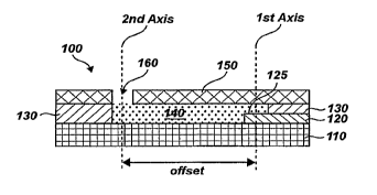
[0007] Figure 1 is a cross-section view of a reference electrode channel that
is
created using a flex circuit according to an embodiment of the invention.
[0008] Figure 2 is a top view of a flex circuit according to an embodiment of
the
invention.
[0009] Figure 3 is a top view of a mask that is used to cover the flex circuit
shown
in figure 2 according to an embodiment of the invention.
[0010] Figure 4 is a top view showing a conductive material deposited into the
opening of the mask according to an embodiment of the invention.
[0011] Figure 5 is a top view of a mask that is used to cover a portion of the
conductive material and the mask shown in figure 4 according to an embodiment
of
the invention.
[0012] Figure 6 is a flow chart showing a method of creating the reference
electrode channel of figure 1 according to an embodiment of the invention.
[0013] Figure 7 is a cross-section view of a reference -electrode channel that
is
created using a flex circuit according to an embodiment of the invention.
[0014] Figure 8 is a top view of a flex circuit according to an embodiment of
the
invention.
[0015] Figure 9 is a top view of a mask that is used to cover the flex circuit
shown
in figure 8 according to an embodiment of the invention.
[0016] Figure 10 is a top view showing a conductive material deposited into
the
opening of the mask according to an embodiment of the invention.
CA 02630541 2008-05-14
WO 2007/100644 PCT/US2007/004696
-4-
[0017] Figure 11 is a top view of a mask that is used to cover the conductive
material and the mask shown in figure 10 according to an embodiment of the
invention.
[0015] Figure 12 is a flow chart showing a method of creating the reference
electrode channel of figure 7 according to an embodiment of the invention.
DETAILED DESCRIPTION
[0019] The invention is directed toward using a flex circuit to create a
reference
electrode channel. The flex circuit has a reference electrode that is masked
and
imaged onto a substrate. A first mask is deposited on the substrate. The first
mask
may have an opening that has a first end that exposes a portion of the
reference
electrode and a second end that exposes a portion of the substrate. The
opening
forms a reference electrode channel. A conductive material may be deposited
into
the opening of the first mask. A second mask is deposited on the first mask
and the
conductive material. The second mask may have an opening that exposes a
portion
of the conductive material that is over the substrate.
[0020] Figure 1 is a cross-section view of a reference electrode channel that
is
created using a flex circuit according to an embodiment of the invention. The
flex
circuit 100 may include a substrate I 10, a trace 120, and a reference
electrode 125.
The trace 120 and the reference electrode 125 may be masked and imaged onto
the
substrate 105. For example, the trace 120 and the reference electrode 125 may
be
formed on the substrate 105 using screen printing or ink deposition
techniques. The
CA 02630541 2008-05-14
WO 2007/100644 PCT/US2007/004696
-5-
trace 120 and the reference electrode 125 may be made of a carbon, copper,
gold,
graphite, platinum, silver-silver chloride, rodium, or palladium material.
[0021] A first mask 130 may be applied or deposited over a portion of the
substrate 110 and over the trace 120. The first mask 130 may have an opening
135
that expose a portion of the reference electrode 125 and a portion of the
substrate
110. The opening 135 forms the reference electrode channel. A conductive
material
140 is deposited in the opening 135 to cover the exposed portion of the
reference
electrode 125 and the exposed portion of the substrate 110. A second mask 150
may
be applied or deposited over the first mask 130 and the conductive material
140.
The second mask 150 may have an opening 160 over a portion of the conductive
material 140 that is over the substrate 110. The opening 135 is positioned
along a
first axis or plane and the opening 160 is positioned along a second axis or
plane.
The first axis or plane is not coincident with the second axis or plane.
Hence, the
first axis or plane is vertically and/or horizontally offset from the second
axis or
plane.
[00221 The opening 160 is the measurement site and allows a fluid of interest
(e.g., blood, urine, etc.) to come into contact with the conductive material
140 to
complete the measurement circuit with another measuring electrode (not show)
in
contact with the same fluid. The conductive material 140 stabilizes the
reference
potential in several ways. The conductive material 140 may provide known
silver
and chloride ion activity, for example, (in the case of a silver-silver
chloride
reference design) to maintain a stable potential. The conductive material 140
should
offer sufficient diffusion resistance to inhibit loss of desired ions to the
fluid of
CA 02630541 2008-05-14
WO 2007/100644 PCT/US2007/004696
-6-
interest, while simultaneously inhibiting migration of unwanted ions toward
the
active surface of the reference electrode 125. Spacing the opening 160 a
sufficient
distance from the reference electrode 125, as shown in figure 1, enhances this
diffusion resistance. Finally, the conductive material 140 may provide a
predictable
junction potential at the interface with the fluid of iinterest which
facilitates accurate
electrochemical measurements using the reference electrode 125.
[0023] Figure 2 is a top view of a flex circuit 100 according to an embodiment
of
the invention. The trace 120 and the reference electrode 125 may be made of a
conductive material such as a silver-silver chloride (Ag / AgCI) material and
may be
formed on the substrate 110 using photolithography or printing techniques
(610).
For example, the trace 120 and the reference electrode 125 may be formed on
the
substrate 110 using screen printing or ink deposition techniques. The
substrate 110
may be a flexible dielectric substrate such as a polyimide. The trace 120 may
be
used to connect to a measurement device (not shown) such as a potentiostat.
The
trace 120 is used to measure a potential from the reference electrode 125
using the
measurement device. Even though figure l shows the flex circuit 100 having one
trace 120 and one reference electrode 125, the flex circuit 100 may have more
than
one, trace and more than one electrode.
[0024] Figure 3 is a top view of a mask 130 that is used to cover the flex
circuit
100 shown in figure 2 according to an embodiment of the invention. The mask
130
may be made of a dielectric material such as a photoimagable epoxy or an
ultraviolet
curable epoxy material. The mask 130 is deposited over the substrate 110 and
has a
rectangular opening 135 that has a first end 135a that exposes a portion of
the
CA 02630541 2008-05-14
WO 2007/100644 PCT/US2007/004696
-7-
reference electrode 125 and a second end 135b that exposes a portion of the
substrate 110 (620). The rectangular opening 135 may have a length of between.
about 0.10-0.20 inches and a width of between about 0.010-0.020 inches. The
length-to-width ratio of the rectangular openirig 135 may be in the range of
between
about 4:1 to 12:1. In one embodiment, the mask 130 covers the entire top
surface of
the flex circuit 100 except for the rectangular opening 135. The mask 130 may
have
a thickness of between about 0.005 inches and about 0.02 inches. The first end
135a
of the opening 135 is positioned directly above the electrode 125 so that the
electrode 125 is exposed or visible through the opening 135 of the mask 130.
Lithography techniques may be used to deposit or place the mask 130 on the
flex
circuit 100.
[00251 Figure 4 is a top view showing a conductive material 140 deposited into
the opening 135 of the mask 130 according to an embodiment of the invention.
The
conductive material 140 is deposited in the opening 135 to cover and to come
into
direct contact with the exposed portion of the reference electrode 125 and the
exposed portion of the substrate 110 (630). The conductive material 140 may be
a
conductive fluid, a conductive solution, a conductive gel, a salt containing
gel, a
conductive polymer containing potassium chloride (KCI) with a small amount of
silver ion (Ag+), or a material having conductive properties. For the case of
a silver-
silver chloride reference electrode 125, addition of a trace of silver nitrate
solution to
a matrix containing potassium chloride precipitates some amount of silver
chloride
within the conductive matrix, but maintains a silver ion concentration at a
constant
amount according to the solubility product of silver chloride, which is 1.56 x
10"'0
CA 02630541 2008-05-14
WO 2007/100644 PCT/US2007/004696
-8-
[0026] Figure 5 is a top view of a mask 150 that is used to cover a portion of
the
conductive material 140 and the mask 130 shown in figure 4 according to an
embodiment of the invention. The mask 150 may be made of a dielectric material
such as a photoimagable epoxy or an ultraviolet curable epoxy material. The
mask
150 has an opening 160 that exposes a portion of the conductive material 140
that
forms a working surface to receive a fluid of interest (640). Lithography
techniques
may be used to deposit or place the mask 150 on the mask 130 and the
conductive
material 140.
[0027] Figure 7 is a cross-section view of a reference electrode channel that
is
created using a flex circuit according to an embodiment of the invention. The
flex
circuit 200 may include a substrate 210, traces 220 and 230, a reference
electrode
225, and a working electrode 235. The traces 220 and 230, the reference
electrode
225, and the working electrode 235 may be masked and imaged onto the substrate
210. For example, the traces 220 and 230, the reference electrode 225, and the
working electrode 235 may be formed on the substrate 210 using screen printing
or
ink deposition techniques. The traces 220 and 230, the reference electrode
225, and
the working electrode 235 may be made of a carbon, copper, gold, graphite,
platinum, silver-silver chloride, rodium, or palladium material.
[0028] A first mask 240 may be applied or deposited over a portion of the
substrate 210 and over the traces 220 and 230. The first mask 240 may have an
opening 250 that expose a portion of the reference electrode 225, a portion of
the
working electrode 235, and a portion of the substrate 210. The term "channel"
(shown as channel 255) may be used to refer to the portion between the
reference
CA 02630541 2008-05-14
WO 2007/100644 PCT/US2007/004696
-9-
electrode 225 and the working electrode 235. Hence, the opening 250 may form
the
reference electrode channel. A conductive material 260 is deposited in the
opening
250 to cover and to come into direct contact with the exposed portion of the
reference electrode 225 and up to the edge of the exposed portion of the
substrate
210. A second mask 265 may be applied or deposited over the first mask 240 and
the conductive materia1260. The second mask 265 may have an opening 270 over a
portion of the working electrode 235. The reference electrode 225 is
positioned
along a first axis or plane and the working electrode 235 is positioned along
a
second axis or plane. The first axis or plane is not coincident with the
second axis or
plane. Hence, the first axis or plane is vertically and/or horizontally offset
from the
second axis or plane.
[00291 The opening 270 is the measurement site and allows a fluid of interest
(e.g., blood, urine, etc.) to come into contact with the working electrode 235
and the
conductive material 260 for a more accurate measurement. The conductive
material
260 stabilizes the reference potential in several ways. The conductive
material 260
may provide known silver and chloride ion activity for example (in the case of
a
silver-silver chloride reference design) to maintain a stable potential. The
conductive material 260 should offer sufficient diffusion resistance to
inhibit loss of
desired ions to the solution, while simultaneously inhibiting migration of
unwanted
ions toward the active surface of the reference electrode 225. Spacing the
opening
270 a sufficient distance from the reference electrode 225, as shown in figure
7,
enhances this diffusion resistance. In addition, the opening 270 communicates
directly with the end of the conductive material 260 at a smaller opening 275.
The
CA 02630541 2008-05-14
WO 2007/100644 PCT/US2007/004696
-10-
proximity of the smaller opening 275 to the working electrode 235 makes this
embodiment ideal for situations where the solution resistance between the
reference
electrode and the working electrode needs to be keep at a minimum, such as in
the
case of a 3-electrode amperometric cell, for example.
[00301 Figure 8 is a top view of a flex circuit 100 according to an embodiment
of
the invention. The traces 220 and 230, the reference electrode 225 and the
working
electrode 235 may be made of a conductive material such as a copper material,
a
platinum material, a silver-silver chloride (Ag / AgCI) material and are
formed on
the substrate 210 using masking and photolithography techniques (1210). For
example, the traces 220 and 230, the reference electrode 225, and the working
electrode 235 may be formed on the substrate 210 using screen printing or ink
deposition techniques. The substrate 210 may be a flexible dielectric
substrate such
as a polyimide. The traces 220 and 230 may be used to connect to a measurement
device (not shown) such as a potentiostat. The traces 220 and 230 may be used
to
carry voltage or current from the reference electrode 225 and the working
electrode
235 to the measurement device.
[0031] Figure 9 is a top view of a mask 240 that is used to cover the flex
circuit
200 shown in figure 8 according to an embodiment of the invention. The mask
240
may be made of a dielectric material such as a photoimagable epoxy or an
ultraviolet
curable epoxy material. The mask 240 is deposited over the substrate 210 and
has a
rectangular opening 250 that has a first end 250a that exposes a portion of
the
reference electrode 225, a second end 250b that exposes a portion of the
working
electrode 235, and a channel or an area 255 between the reference electrode
225 and
CA 02630541 2008-05-14
WO 2007/100644 PCT/US2007/004696
-11-
the working electrode 235 that exposes a portion of the substrate 210 (1220).
The
rectangular opening 250 may have a length of between about 0.10-0.20 inches
and a
width of between about 0.010-0.020 inches. The length-to-width ratio of the
rectangular opening 250 may be in the range of between about 4:1 to 12:1. In
one
embodiment, the mask 240 covers the entire top surface of the flex circuit 210
except for the rectangular opening 250. The mask 240 may have a thickness of
between about 0.005 inches and about 0.02 inches. In one embodiment, the first
end
250a of the opening 250 is positioned directly above the reference electrode
225 so
that the reference electrode 225 is exposed or visible through the opening 250
of the
mask 240. In one embodiment, the second end - 250b of the opening 250 is
positioned directly above the working electrode 235 so that the working
electrode
235 is exposed or visible through the opening 250 of the mask 240. Lithography
techniques may be used to deposit or place the mask 240 on the flex circuit
200.
[0032] Figure 10 is a top view showing a conductive material 260 deposited
into
the opening 250 of the mask 240 according to an embodiment of the invention.
The
conductive material 260 is deposited in the opening 250 to cover and to come
into
direct contact with the exposed portion of the reference electrode 225 and in
the area
255 between the reference electrode 225 and the working electrode 235 (i.e.,
on the
exposed portion of the substrate 210) (1230). In one embodiment, a screenable
gel
or a conductive polymer is applied in the opening 250 to cover and to come
into
direct contact with the exposed portion of the reference electrode 225 and in
the area
255 between the reference electrode '225 and the working electrode 235. The
conductive material 260 may be a conductive fluid, a conductive solution, a
CA 02630541 2008-05-14
WO 2007/100644 PCT/US2007/004696
-12-
conductive gel, a salt containing gel, a conductive polymer containing
potassium
chloride (KCI) with a small amount of silver ion (Ag+), or a material having
conductive properties. The conductive material 260 may form a salt channel or
a
reference electrode channel.
[0033] Figure 11 is a top view of a mask 265 that is used to cover the
conductive
material 260 and the mask 240 shown in figure 10 according to an embodiment of
the invention. The mask 265 may be made of a dielectric material such as a
photoimagable epoxy or an ultraviolet curable epoxy material. The mask 265 has
an
opening 270 that exposes a portion of the working electrode 235 and an edge of
the
conductive material 260, which forms a space to receive a fluid of interest.
Lithography techniques may be used to deposit or place the mask 265 on the
mask
240 and the conductive material 260 (1240).
[0034] While certain exemplary embodiments have been described and shown in
the accompanying drawings, it is to be understood that such embodiments are
merely illustrative of and not restrictive on the broad invention, and that
this
invention not be limited to the specific constructions and arrangements shown
and
described, since various other changes, combinations, omissions, modifications
and
substitutions, in addition to those set forth in the above paragraphs, are
possible_
Those skilled in the art will appreciate that various adaptations and
modifications of
the just described embodiments can be configured without departing from the
scope
and spirit of the invention. Therefore, it is to be understood that, within
the scope of
the appended claims, the invention may be practiced other than as specifically
described herein.