Note: Descriptions are shown in the official language in which they were submitted.
CA 02630792 2008-05-22
DESCRIPTION
Diamond Electrode, Method for Producing Same, and Electrolytic Cell
TECHNICAL FIELD
The present invention relates to a diamond electrode employed for sewage
disposal or formation of functional water and a method for producing the same.
The
present invention also relates to an electrolytic cell employing this diamond
electrode,
employed for formation of ozone water or the like.
BACKGROUND ART
Electrolyzation (hereinafter referred to as "electrolysis") of water is
performed
for producing electrolytic water employed in the fields of medical care and
food or for
cleaning electronic components, or for wastewater treatment. For example,
electrolysis of water is known as a method for producing water in which ozone
is
dissolved, i.e., the so-called ozone water.
The ozone water is a kind of functional water, has extremely strong oxidizing
power, and is utilized in various fields of medical care, cleaning of
electronic devices etc,
as sterilizing water or cleaning water through the oxidizing power. In order
to form
ozone water by dissolving ozone gas in water, an apparatus for generating
impurity-free
ozone gas and dissolving the same in water is necessary, and the apparatus is
increased
in size and complicated, while it is difficult to obtain high-purity ozone
water.
According to a method for forming ozone water by electrolyzing pure water,
however,
the apparatus can be easily downsized, and high-purity ozone water can be
easily
obtained.
Lead dioxide, platinum or the like excellently functioning as a catalyst is
known
as the material for an electrode employed for this electrolysis. However, this
material
has a problem of elution of the electrode, and an apparatus for removing
eluted metallic
impurities must be provided when high-purity ozone water is required, to
complicate the
-1-
CA 02630792 2008-05-22
apparatus.
Therefore, a conductive diamond supplied with conductivity through addition of
a dopant such as boron has recently been attracted attention as an electrode
material
substituting for the aforementioned material. The conductive diamond is
chemically
extremely stable, not eluted in electrolysis and has a wide potential window,
whereby
ozone can be electrolytically generated from pure water having high electrical
resistance
with an electrode (hereinafter referred to as "diamond electrode") employing
this
conductive diamond.
As this diamond electrode, Japanese Patent Laying-Open No. 2005-336607
(Patent Document 1), for example, discloses an electrode obtained by
perforating and
meshing a self-supporting membrane of diamond prepared by chemical vapor
deposition
(CVD) in order to increase the surface area of the electrode and improve
electrolytic
efficiency. However, a long synthesis time is required for preparing this
diamond self-
supporting membrane to result in a high cost, while the diamond self-
supporting
membrane is easily warped and easily forms a clearance between the same and an
ion-
exchange membrane. Further, the step of meshing the membrane with a laser also
results in a high cost.
Therefore, a diamond electrode obtained by forming a membrane of conductive
diamond on a meshed or porous substrate consisting of a valve metal such as
titanium or
niobium by CVD is proposed, and disclosed in Japanese Patent Laying-Open No. 9-
268395 (Patent Document 2), Japanese Patent Laying-Open No. 2001-192874
(Patent
Document 3) or the like, for example. However, the thermal expansion
coefficient of
the substrate consisting of titanium or niobium is remarkably different from
that of
diamond, whereby the electrode easily cause remarkable residual stress
resulting from
the difference in thermal expansion coefficient between the same and diamond
when in
use. Consequently, the conductive diamond and the substrate are easily
separated from
each other, to disadvantageously reduce the life of the electrode.
As a substrate for forming a diamond electrode by covering conductive diamond
-2-
CA 02630792 2008-05-22
by CVD, a conductive silicon substrate is also known. The difference in
thermal
expansion coefficient between the conductive silicon substrate and diamond is
relatively
small, whereby the conductive silicon substrate has a small problem of
separation
resulting from residual stress. However, it is difficult to form a mesh
structure with
conductive silicon. In other words, while a substrate of a mesh structure can
be easily
produced by a method laterally pulling a flat plate provided with a large
number of small
pores in the case of titanium or niobium, this method cannot be applied to
conductive
silicon, and only a flat conductive silicon substrate has been present in
general.
Therefore, no porous diamond electrode employing a conductive silicon
substrate has
been obtained.
Patent Document 1: Japanese Patent Laying-Open No. 2005-336607
Patent Document 2: Japanese Patent Laying-Open No. 9-268395
Patent Document 3: Japanese Patent Laying-Open No. 2001-192874
DISCLOSURE OF THE INVENTION
PROBLEMS TO BE SOLVED BY THE INVENTION
An object of the present invention is to provide a diamond electrode prepared
by
covering a substrate with conductive diamond, having a low production cost, no
problem of warping and a large electrode surface area, capable of obtaining
high
electrolytic efficiency, hardly causing separation between the conductive
diamond
(diamond cover layer) and the substrate and having a long practicable life and
a method
for producing the same.
Another object of the present invention is to provide an electrolytic cell
allowing
easy downsizing of an apparatus, using the diamond electrode according to the
present
invention, employed for formation of ozone water or the like for attaining
high
electrolytic efficiency and having a long practicable life.
MEANS FOR SOLVING THE PROBLEMS
As a result of a deep study, the inventors have found that a plurality of
pores can
be formed in a flat silicon substrate by ion etching, solution etching with
fluoronitric acid
-3-
CA 02630792 2008-05-22
or sandblasting and that a diamond electrode capable of attaining high
electrolytic
efficiency and hardly causing separation between a diamond cover layer and a
substrate
can be obtained by covering the surface of a conductive silicon substrate
having a
plurality of pores formable in this manner with conductive diamond, and
completed the
present invention on the basis of this recognition.
The diamond electrode according to the present invention comprises a
conductive silicon substrate having a plurality of pores and a conductive
diamond
covering this conductive silicon substrate.
Preferably in the diamond electrode according to the present invention, the
said
conductive diamond (1) covers at least 90 % of the surfaces of the conductive
silicon
substrate, or (2) covers only a first surface of the conductive silicon
substrate.
Preferably in the diamond electrode according to the present invention, the
inner
wall surfaces of the said plurality of pores are at an angle of 45 to 85
with respect to
the substrate surface of the said conductive silicon substrate.
Preferably in the diamond electrode according to the present invention, the
said
plurality of pores have tapered inner walls, and the open area of the pores on
a first
substrate surface is smaller than the open area of the pores on a second
substrate surface.
More preferably, the open area ratio of the said plurality of pores is 3 to 80
% on the
respective substrate surfaces in this case.
Preferably in the diamond electrode according to the present invention, at
least
60 % of the said plurality of pores on each substrate surface have open areas
in the
range of difference of 10 % from each other.
Preferably in the diamond electrode according to the present invention, the
aspect ratio of the said plurality of pores is 0.2 to 3.
The present invention also provides a method for producing the aforementioned
diamond electrode according to the present invention, including the step of
covering the
said conductive silicon substrate with the conductive diamond by chemical
vapor
deposition.
-4-
CA 02630792 2011-03-31
The present invention also provides an electrolytic cell comprising a cation-
exchange membrane, an anode and a cathode provided in close contact with both
surfaces of the said cation-exchange membrane respectively and collectors
provided in
contact with the said anode and the cathode in an electrically feedable
manner,
characterized in that at least the said anode is composed of the
aforementioned diamond
electrode according to the present invention, and the said collectors are
composed of a
conductive nonmetal allowing permeation of an electrolyte.
The present invention further provides an electrolytic cell comprising a
diaphragm separating the cell into two chambers as well as an anode and a
cathode
provided in the first and second chambers separated by this diaphragm
respectively,
characterized in that the said anode is composed of the aforementioned diamond
electrode according to the present invention.
According to an aspect of the present invention there is provided a diamond
electrode comprising a conductive silicon substrate having a plurality of
pores; and a
conductive diamond covering said conductive silicon substrate, wherein the
inner wall
surfaces of said plurality of pores are at an angle of 60 to 85 with respect
to a substrate
surface of said conductive silicon substrate.
According to another aspect of the present invention there is provided a
method
of producing a diamond electrode as described herein, the method comprising
the steps
of:
forming the plurality of pores of said conductive silicon substrate, having an
inner wall
surface at an angle of 60 to 85 with respect to the substrate surface of
said conductive
silicon substrate by ion etching, solution etching with fluoronitric acid or
sandblasting;
and
covering said conductive silicon substrate having a plurality of pores formed
with
conductive diamond by chemical vapor deposition.
According to a further aspect of the present invention there is provided an
electrolytic cell comprising:
a cation-exchange membrane;
an anode and a cathode provided in close contact with both surfaces of said
cation-
exchange membrane respectively; and
collectors provided in contact with said anode and said cathode in an
electrically
feedable manner;
-5-
CA 02630792 2011-03-31
wherein at least said anode is composed of a diamond electrode as provided
herein, and
wherein said collectors are composed of a conductive nonmetal allowing
permeation of
an electrolyte.
EFFECTS OF THE INVENTION
The diamond electrode according to the present invention has a low production
cost and no problem of warping, can obtain high electrolytic efficiency,
hardly causes
separation between a diamond cover layer constituting the same and the
conductive
silicon substrate, and has a long practicable life also in formation of ozone
water or the
like. This diamond electrode can be easily produced by the method according to
the
present invention. The electrolytic cell according to the present invention is
an
electrolytic cell allowing easy downsizing of an apparatus and has an
electrode capable
of attaining high electrolytic efficiency and a long life, whereby the same
can be suitably
employed for formation of ozone water by electrolysis of water or the like.
BRIEF DESCRIPTION OF THE DRAWINGS
Fig. I is a sectional view schematically showing a preferred diamond electrode
I
according to the present invention.
Figs. 2(a) and 2(b) are a top plan view and a bottom plan view of diamond
electrode 1 shown in Fig. 1.
Fig. 3 is a sectional view schematically showing another exemplary preferred
-5a-
CA 02630792 2008-05-22
diamond electrode 11 according to the present invention.
Fig. 4 is a sectional view schematically showing still another exemplary
preferred
diamond electrode 21 according to the present invention.
Fig. 5 is a sectional view schematically showing an exemplary preferred
electrolytic cell 31 employing diamond electrode 11 according to the present
invention.
Fig. 6 is a sectional view schematically showing another exemplary preferred
electrolytic cell 51 employing diamond electrode 11 according to the present
invention.
DESCRIPTION OF THE REFERENCE SIGNS
1, 11, 21 diamond electrode, 2, 22 conductive silicon substrate, 3, 12, 23
conductive diamond (diamond cover layer), 4, 24 pore, 31, 51 electrolytic
cell, 32
cation-exchange membrane, 33 anode, 34 cathode, 35, 36 collector, 37
electrolytic cell case, 38, 40, 55, 56 inlet, 39, 41, 59, 60 outlet, 42, 43,
53, 54 lead
wire, 52 diaphragm, 57, 58 electrolyte.
BEST MODES FOR CARRYING OUT THE INVENTION
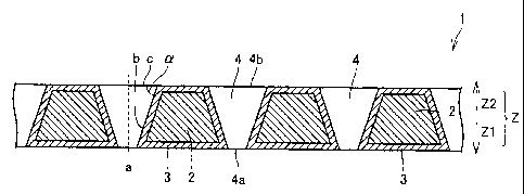
Fig. 1 is a sectional view schematically showing an exemplary preferred
diamond
electrode 1 according to the present invention, and Figs. 2(a) and 2(b) are a
top plan
view and a bottom plan view of diamond electrode 1 shown in Fig. 1
respectively. Fig.
1 is a sectional view taken along the cutting plane line I-I in Fig. 2(a).
Diamond
electrode 1 according to the present invention comprises a conductive silicon
substrate 2
having a plurality of pores 4 and a conductive diamond (diamond cover layer) 3
covering conductive silicon substrate 2.
Conductive silicon substrate 2 in the present invention means a substrate
consisting of silicon supplied with conductivity. "Conductivity" indicates
that
resistivity is not more than 20 )-cm (preferably not more than 1.0 Q=cm). Such
conductivity can be supplied by adding (doping) boron or the like to the
substrate
material. The thermal expansion coefficients of conductive silicon substrate 2
and the
conductive diamond described later are relatively close to each other, whereby
residual
stress resulting from thermal expansion coefficient difference is reduced,
separation of
-6-
CA 02630792 2008-05-22
the diamond can be suppressed and a practicable long life can be attained by
employing
a substrate of conductive silicon as the substrate covered with the diamond.
Conductive silicon substrate 2 in the present invention has plurality of pores
4.
While "plurality of' means at least two, conductive silicon substrate 2
according to the
present invention specifically has a large number of pores of 0.1 to 100/cm2
(more
preferably, 0.5 to 10/cm2), as shown in Examples described later. In diamond
electrode
I according to the present invention prepared by covering conductive silicon
substrate 2
having such plurality of pores 4 with conductive diamond 3, the upper surface
(Fig.
2(a)) and the lower surface (Fig. 2(b)) thereof are meshed.
A circular shape, a quadrangular shape such as a rhomboid shape, a triangular
shape or another polygonal shape can be listed as the opening shape of pores 4
provided
in conductive silicon substrate 2. While the opening shape may be an
indeterminate
shape or a mixture of these shapes, a shape enabling a formed gas to easily
escape from
the pores is preferable since contact between an electrolyte such as pure
water and the
electrode or the ion-exchange membrane is hindered, distribution is caused in
electrolysis and the electrolytic efficiency is reduced if a gas, such as
hydrogen gas, for
example, formed by electrolytic reaction remains in pores 4.
Pores 4 can be formed by ion etching, solution etching with fluoronitric acid
or
sandblasting. The conductive silicon is hard to mesh by a method laterally
pulling a flat
plate provided with a large number of small pores dissimilarly to niobium or
titanium,
and it has generally been impossible to obtain a meshed or porous conductive
silicon
substrate. However, conductive silicon substrate 2 having the plurality of
pores can be
obtained by the aforementioned method, and diamond electrode 1 according to
the
present invention has been obtained.
Ion etching is a method for etching the substrate by colliding ions against
the
conductive silicon substrate. Solution etching with fluoronitric acid is a
method for
etching the conductive silicon substrate by dissolving silicon with a
fluoronitric acid
solution. Sandblasting is a method for mechanically polishing the substrate by
colliding
-7-
CA 02630792 2008-05-22
hard particles of alumina or the like against the conductive silicon
substrate. The
plurality of pores passing through the conductive silicon substrate in
relation to the
thickness direction thereof can be formed by employing any of these methods.
More
specifically, portions of the conductive silicon substrate other than those
for forming the
pores are covered with a mask, and ion etching, solution etching with
fluoronitric acid
or sandblasting is performed. A mask of resin or metal is illustrated as the
mask.
While ion etching, solution etching with fluoronitric acid or sandblasting is
performed
until through-holes are formed, the shape, the size, the open area ratio, the
taper angle
and the aspect ratio of the pores described later can be adjusted by varying
the shape of
the mask and the conditions for ion etching, solution etching with
fluoronitric acid or
sandblasting.
Conductive silicon substrate 2 in the present invention can be produced by
employing a proper well-known unporous flat conductive silicon substrate
(commercially available flat conductive silicon substrate, for example) used
as a
substrate for a diamond electrode and forming pores therein in the
aforementioned
method. While the ranges of the thickness and the size of conductive silicon
substrate
2 in the present invention vary with the size of the electrode etc. and are
not particularly
restricted, a thickness causing no warping of the electrode (more
specifically, in the
range of 0.5 to 10 mm) is required.
Diamond electrode 1 according to the present invention is characterized in
that
the aforementioned conductive silicon substrate 2 is covered with conductive
diamond 3.
"Cover" means such a state that the diamond is chemically or physically in
close contact
with the silicon substrate to cover the same. In diamond electrode 1 according
to the
present invention, the surfaces of the conductive silicon substrate (including
the inner
wall surfaces of the pores, in addition to both main surfaces and the side
surfaces of the
substrate) are partially or entirely covered with the conductive diamond. In
this
specification, the layer of the conductive diamond covering the conductive
silicon
substrate is referred to as "diamond cover layer".
-8-
CA 02630792 2008-05-22
When all surfaces of the conductive silicon substrate are covered with the
conductive diamond in the diamond electrode according to the present
invention, the
surface area of the diamond cover layer is increased due to the plurality of
pores
provided in the conductive silicon substrate, and electrolytic efficiency is
improved.
When only a surface (described later) so provided as to come into contact with
the ion-
exchange membrane is covered with the conductive diamond in both surfaces of
the
conductive diamond substrate, it follows that a plurality of three-phase
contact portions
of pure water (electrolyte), the ion-exchange membrane and the diamond
electrode are
formed due to the plurality of pores provided in the conductive silicon
substrate, to
enable electrolysis of pure water or the like having high electrical
resistance. In this
specification, the electrolyte means a liquid subjected to the electrolysis,
and includes
pure water or extrapure water having high electrical resistance.
The "conductivity" of the conductive diamond in the present invention
indicates
that the resistivity is not more than 20 f). cm (preferably not more than 1.0
Q -cm),
similarly to the aforementioned "conductivity" of the silicon substrate. Such
conductivity is supplied by adding a dopant (impurity) to the diamond. While
phosphorus, nitrogen, boron or sulfur can be listed as the dopant added to the
diamond
for supplying conductivity, the type thereof is no object if the same is an
element having
a valence different from that of carbon and capable of supplying conductivity.
However, boron or phosphorus is added in general, and the content thereof is
preferably
1 to 10000 ppm, more preferably 100 to 10000 ppm. Boron oxide or diphosphorus
pentaoxide having small toxicity can be preferably used as the raw material
for this
added element.
While the thickness of diamond cover layer 3 in diamond electrode 1 according
to the present invention varies with conditions, environment etc. for use of
the electrode
and is not particularly restricted, this thickness is preferably 3 to 100 m
in view of
easiness in production and the cost. If the thickness of diamond cover layer 3
is less
than 3 m, there is a possibility that the silicon substrate is partially not
covered with the
-9-
CA 02630792 2008-05-22
diamond. If the thickness of diamond cover layer 3 exceeds 100 p.m, on the
other hand,
the thickness may be excessive, to increase the cost.
In the diamond electrode according to the present invention, the conductive
diamond preferably covers at least 90 % of the surfaces of the conductive
silicon
substrate. When electrolyzing a conductive electrolyte such as an aqueous
solution in
which sulfuric acid, sodium sulfate, sodium carbonate or fluoric acid is
dissolved, the
diamond electrode is generally not provided in close contact with the ion-
exchange
membrane or the like but used in a state where all surfaces thereof are
directly in contact
with the conductive electrolyte. In this case, wider surfaces of the
conductive silicon
substrate are preferably covered with the conductive diamond, in order to
improve the
electrolytic efficiency. When the electrolyte is an aqueous fluoric acid
solution or the
like dissolving silicon, dissolution of silicon can be prevented by covering
the surfaces of
the conductive silicon substrate with the conductive diamond, and wider
surfaces of the
conductive silicon substrate are preferably covered with the conductive
diamond also in
such a point of view.
More specifically, areas of at least 90 % of the surfaces of the substrate are
preferably covered, and all surfaces (100 % of the surfaces) of conductive
silicon
substrate 2 are particularly preferably covered with diamond cover layer 3, as
in the
example shown in Figs. 1 and 2.
Fig. 3 is a sectional view schematically showing another exemplary preferred
diamond electrode 11 according to the present invention. Diamond electrode 11
of the
example shown in Fig. 3 has a structure similar to that of diamond electrode 1
of the
example shown in Fig. 1 except a part, and portions having similar structures
are
denoted by the same reference signs, to omit redundant description. Diamond
electrode 11 of the example shown in Fig. 3 is characterized in that a
conductive
diamond (diamond cover layer 12) covers only a first surface (more
specifically, only a
surface of a first (Z 1) side in a thickness direction Z of diamond electrode
11) of a
conductive silicon substrate 2.
-10-
CA 02630792 2008-05-22
When an electrolyte is prepared from pure water or extrapure water having high
electrical resistance, the diamond electrode is so provided and used as to be
in close
contact with an ion-exchange membrane. As a method for directly forming ozone
water by electrolyzing pure water or the like, for example, and an excellent
method
capable of easily downsizing an apparatus, a method for directly forming ozone
water by
electrolyzing pure water or the like with an electrolytic cell formed by
holding an ion-
exchange membrane between an anode and a cathode is disclosed in Fig. 2 etc.
of
Japanese Patent Laying-Open No. 52-78788. A diamond electrode employed for the
anode or the like in this method disclosed in Japanese Patent Laying-Open No.
52-
78788 is so provided and used as to be in close contact with the ion-exchange
membrane.
As a result of a deep study, the inventors have found that, when the diamond
electrode is so provided and used as to be in close contact with the ion-
exchange
membrane (i.e., in the case of electrolysis of pure water or the like having
high electrical
resistance), electrolytic reaction such as reaction of ozone generation is
caused only on a
zone (three phase zone) where the three phases of the ion-exchange membrane,
the
anode wall surface (surface exposing the conductive diamond) and the pure
water are in
contact with each other and a portion of the electrode not in contact with the
ion-
exchange membrane does not contribute to the reaction, whereby the electrode
can
sufficiently function as the electrode also when only the first surface of the
conductive
silicon substrate is covered with the conductive diamond.
Even when the conductive silicon substrate is directly in contact with the
electrolyte, silicon is hardly dissolved in the electrolyte such as pure water
when pure
water or the like having high electrical resistance is electrolyzed, if the
conductive silicon
substrate is not in contact with the ion-exchange membrane. Therefore, diamond
cover
layer 12 is preferably so formed as to cover only the first surface of
conductive silicon
substrate 2 as in diamond electrode 11 of the example shown in Fig. 3, in
consideration
of easiness in production and the cost.
-11-
CA 02630792 2008-05-22
In diamond electrode 1 according to the present invention, the inner wall
surfaces of the said plurality of pores 4 are preferably at an angle of 45 to
90 with
respect to the said substrate surface. The angle (referred to as "taper angle"
in this
specification) of the inner wall surfaces with respect to the substrate
surface is an angle
(angle (x in Fig. 1) formed by, on a section (surface perpendicular to the
plane of Fig. 1)
including a center line (center line a in Fig. 1) passing through each pore 4,
a nodal line
(nodal line b in Fig. 1) between this section and the inner wall and a plane
(plane c in Fig.
1) extending the substrate surface (main surface) of conductive silicon
substrate 2 to the
opening of the pore.
When pores 4 are tapered as described later (in the case of the example shown
in
Fig. 1 or 3), the difference between opening diameters of the pores on both
main
surfaces of the conductive silicon substrate is excessively increased if the
taper angle is
less than 45 , and penetration of the pores may generally be difficult when
the larger
opening diameter is set in a practical range. If the pores are shaped as shown
in Fig. 4
(described later), sections of the pores at the center of the conductive
substrate in the
thickness direction may be so excessively reduced that it is difficult to
discharge bubbles
resulting from the electrolysis. If the taper angle exceeds 90 , on the other
hand, the
pores are unpreferably shaped to hinder discharge of the bubbles resulting
from the
electrolysis.
In diamond electrode 1 or 11 according to the present invention, the said
taper
angle is more preferably 60 to 85 . If the said taper angle is less than 60 ,
the
difference between the opening diameters of the pores on both surfaces of the
substrate
is remarkable when the pores are tapered and the smaller opening diameter may
generally be so excessively reduced that it is difficult to set the same to a
practical size
when the larger opening diameter is set in a practical range, while the
sections of the
pores at the center of the substrate in the thickness direction may be so
small that
bubbles resulting from the electrolysis hardly escape also when the pores are
shaped as
shown in Fig. 4 (described later). On the other hand, bubbles resulting from
the
-12-
CA 02630792 2008-05-22
electrolysis so hardly escape that the electrolytic efficiency tends to lower
with respect
to supplied power if the said taper angle exceeds 85 , and hence the said
taper angle is
preferably not more than 85 , in order to more effectively exhibit the
function of the
electrode. In the case of preparing the diamond electrode by covering all
surfaces of
the substrate with the conductive diamond, it is difficult to form the diamond
cover layer
on the inner wall surfaces by CVD and such a problem easily arises that the
diamond
cover layer on the inner wall surfaces is reduced in thickness or the inner
wall surfaces
are not entirely covered if the taper angle exceeds 85 . Therefore, the said
taper angle
is preferably not more than 85 , also in this point of view. More preferably,
the taper
angle is not more than 70 , or not more than 80 . Figs. 1 to 3 show such cases
that the
inner walls of pores 4 are in contact with substrate surfaces on second sides
Z2 in the
thickness directions with taper angles of about 70 .
While the taper angles of all pores provided in the conductive silicon
substrate
are preferably in the aforementioned range in the diamond electrode according
to the
present invention, at least 70 % of the pores provided in the conductive
silicon substrate
may be so implemented as to have at least the said taper angle. The diamond
electrode
according to the present invention having a plurality of pores having such a
preferable
taper angle can be produced by gradually engraving the conductive silicon
substrate
from the side of one surface by the aforementioned ion etching, solution
etching with
fluoronitric acid or sandblasting.
Preferably in diamond electrode 1 according to the present invention, the said
plurality of pores 4 have tapered inner walls, and the open area of the pores
on the first
substrate surface is smaller than the open area of the pores on the second
substrate
surface. "Have tapered inner walls." means that the sectional area of the
pores in a
section parallel to the substrate surfaces increases from the first substrate
surface toward
the second substrate surface. The sectional shape of the pores is not
restricted to a
circular shape. Also when the sectional shape of the pores is a polygonal or
indeterminate shape corresponding to the opening shape, the pores
correspondingly
- 13 -
CA 02630792 2010-06-03
"have tapered inner walls." if the sectional area increases from the first
substrate surface
toward the second substrate surface. Figs. I to 3 show such examples that
conductive
silicon substrates 2 have tapered inner walls and the areas of openings 4a on
first sides
Z I in the thickness directions are so implemented as to be smaller than the
areas of
openings 4b on second sides Z2 in the thickness directions. According to this
structure,
bubbles resulting from the electrolysis easily escape, and high electrolytic
efficiency is
attained.
Pores 4 of conductive silicon substrate 2 have the aforementioned tapered
inner
walls, whereby bubbles formed in the electrolysis easily escape from the
pores, no
distribution is caused in the electrolysis, and the electrolytic efficiency
with respect to
the supplied power is improved. While the present invention also includes a
diamond
electrode 21 prepared by covering all surfaces of a conductive silicon
substrate 22
having a plurality of pores 24 with a conductive diamond (diamond cover layer
23) so
that pores 24 are formed narrower than both opening portions on the centers in
the
thickness direction thereof as shown in Fig. 4, for example, bubbles formed in
electrolysis hardly escape from the pores and electrolytic efficiency tends to
lower as
compared with the examples shown in Figs. 1 to 3 when the pores are not so
shaped as
to "have tapered inner walls" in this manner. Conductive silicon substrate 22
employed
in the example of Fig. 4 can be produced by performing solution etching with
fluoronitric acid or sandblasting on both surfaces of the conductive silicon
substrate.
In the case of such a structure that diamond cover layer 12 covers only the
first
surface of conductive silicon substrate 2 as in the example shown in Fig. 3,
the open
areas of pores 4 are preferably so implemented as to be smaller on the side
(first Z1 side
in the thickness direction) of the main surface of the substrate covered with
diamond
cover layer 12 and to be larger on the opposite side (second Z2 side in the
thickness
direction). Thus, there are such advantages that bubbles formed on the three
phase
zone (zone where the three phases of diamond cover layer 12, the ion-exchange
membrane and pure water are in contact with each other) easily escape from the
pores
-14-
CA 02630792 2008-05-22
into the electrolyte (pure water), no distribution is caused in the
electrolysis, and the
electrolytic efficiency with respect to the supplied power is improved.
When the open area of the pores on the first substrate surface is so
implemented
as to be smaller than the open area of the pores on the second substrate
surface as
described above, it is specifically more preferable that the larger open area
is in the range
of 3 to 80 mm2 (more preferably in the range of 7 to 30 mm2) and the smaller
open area
is in the range of 1.5 to 40 mm2 (more preferably in the range of 3 to 20
mm2).
The preferred diamond electrode according to the present invention in which
the
aforementioned plurality of pores 4 have tapered inner walls and the open area
of the
pores on the first substrate surface is smaller than the open area of the
pores on the
second substrate surface can be produced by performing the aforementioned ion
etching,
solution etching with fluoronitric acid or sandblasting from the side of one
surface of the
conductive silicon substrate.
In the diamond electrode according to the present invention, the open area
ratio
of the plurality of pores provided in the conductive silicon substrate is
preferably 3 to
80 % on the respective substrate surfaces (main surfaces). The "open area
ratio"
means the ratio of the total of the open areas of all pores present on the
outer surface of
the electrode with respect to the electrode area (area including the substrate
main
surfaces and the openings of the pores) when the outer surface of the
electrode is
regarded as a plane. If this open area ratio is 3 to 80 % on each substrate
surface, the
electrolytic efficiency with respect to the supplied power is further
increased, and the
function as the electrode can be more efficiently exhibited. More preferably,
the said
open area ratio is 20 to 40 % on the side having the smaller open area as
described
above, and 30 to 70 % on the side having the large open area. When the pores
have
such open area ratios on the respective substrate surfaces respectively,
higher
electrolytic efficiency can be advantageously attained.
In the diamond electrode according to the present invention, the open areas of
the plurality of pores on the respective substrate surfaces are preferably
substantially
- 15 -
CA 02630792 2008-05-22
identical to each other. In other words, it is preferable that at least 60 %
(more
preferably at least 70 %) of the openings of the said plurality of pores on
the respective
substrate surfaces have open areas different from each other by not more than
10 %
(more preferably not more than 7 %). Thus, the volume of formation of ozone
water
or the like with respect to the supplied power can be easily controlled.
In the diamond electrode according to the present invention, the aspect ratio
of
the said plurality of pores is preferably in the range of 0.2 to 3. The
"aspect ratio" is
the ratio of the depth of the pores with respect to the opening diameter of
the pores.
The opening diameter means the diameter of the pores on the plane where the
pores
open if the pores are circular, while the diameter of a circle having an area
equal to the
open area of the pores is regarded as the open area of the pores if the
openings of the
pores are not circular. While the open areas may be different from each other
between
both substrate surfaces in the diamond electrode according to the present
invention, the
said aspect ratio indicates a value with reference to the opening diameter on
the side
having the larger open area.
If the aspect ratio of the said pores exceeds 3 (in other words, the diameter
of
the pores is excessively small with respect to the thickness of the
substrate), the pores
are so deep that bubbles formed in the electrolysis hardly escape from the
pores.
Consequently, the electrolyte such as pure water hardly comes into contact
with the
conductive diamond, and the electrolytic efficiency tends to lower. If the
aspect ratio
of the said pores is less than 0.2, i.e., when the diameter of the pores is
large with
respect to the thickness of the substrate, on the other hand, the substrate
tends to be
easily broken when covered with the diamond. More preferably, the aspect ratio
is 0.5
to not more than 2Ø Figs. 1 to 3 show such examples that the aspect ratios
with
reference to the opening diameters on the second Z2 sides in the thickness
directions are
about 1.
The diamond electrode according to the present invention can be produced by
covering the surfaces of the said conductive silicon substrate with the
conductive
-16-
CA 02630792 2008-05-22
diamond. Covering with the conductive diamond can be performed by chemical
vapor
deposition (CVD). The present invention also provides a method for producing
this
diamond electrode, including the step of covering the conductive silicon
substrate with
the conductive diamond by CVD, in addition to the aforementioned diamond
electrode.
When producing the diamond electrode (shown in Fig. 1, 2 or 4, for example)
according to the present invention prepared by covering all surfaces of the
conductive
silicon substrate with the conductive diamond, covering with the conductive
diamond by
CVD is preferably performed from the sides of both main surfaces of the
conductive
silicon substrate. In this case, covering may be simultaneously performed, or
covering
may be separately performed as to both main surfaces of the conductive silicon
substrate.
Thus, the inner wall surfaces of pores 4 can also be covered with the
conductive
diamond in a sufficient thickness.
When producing the diamond electrode (shown in Fig. 3, for example) prepared
by covering only the first surface of the conductive silicon substrate with
the conductive
diamond, covering with the conductive diamond by CVD is preferably performed
only
from the first main surface (main surface on the first Z1 side in the
thickness direction in
the example shown in Fig. 3) of the conductive silicon substrate. Also when
CVD is
performed only from the first main surface of the conductive silicon
substrate, pores 4
may be partially covered with the conductive diamond due to extension of
reactive gas.
CVD in the method for producing a diamond electrode according to the present
invention can be performed under conditions similar to those for well-known
diamond
covering by CVD. Hot filament CVD (chemical vapor deposition), microwave
plasma
CVD or the like can be listed as typical CVD.
Hot filament CVD can be performed by holding a carbon containing gas such as
methane or alcohol serving as a carbon source in a reducing atmosphere of
hydrogen gas
or the like in which a substrate (conductive silicon substrate) for carrying
diamond is set,
heating the same to a temperature of 1800 to 2400 C for forming carbon
radicals and
thereafter lowering the temperature of the reducing atmosphere to a level of
750 to
-17-
CA 02630792 2008-05-22
950 C easily depositing diamond. The concentration of the carbon containing
gas with
respect to the hydrogen gas is preferably 0.1 to 10 volume %, while a supply
speed of
0.01 to 1 1/min. and a pressure of 2000 to 100000 Pa are employed in general.
Microwave plasma CVD is a method employing hydrogen plasma generated by a
microwave for etching a non-diamond component. The output of the plasma is
preferably 1 to 5 kW, and a larger number of active species can be generated
and the
growth rate of diamond is increased as the output is increased. According to
this
method, a diamond film can be formed on a substrate having a large surface
area at a
high speed. The pressure in a chamber is 4000 to 15000 Pa, and an introduction
flow
rate of a gas mixture of hydrogen and the carbon source is preferably 10 to
100 ml/min.
in general.
When the conductive silicon substrate is covered with the conductive diamond,
pretreatment (for example, roughening of the conductive silicon substrate
surfaces by
blasting or seeding of applying nanodiamond particles having an average
particle
diameter of 1 to 50 nm onto the conductive silicon substrate with excellent
dispersibility) is preferably so performed as to increase adhesiveness between
the
conductive silicon substrate and the diamond cover layer.
Fig. 5 is a sectional view schematically showing an exemplary preferred
electrolytic cell 31 employing the aforementioned diamond electrode 11
according to the
present invention. The diamond electrode according to the present invention is
employed as an electrode in electrolysis of various electrolytes such as a
conductive
electrolyte and an electrolyte such as pure water having high electrical
resistance.
Particularly in a case of an electrolytic cell for directly forming ozone
water by
electrolyzing pure water with an electrolytic cell constituted of an ion-
exchange
membrane as well as an anode and a cathode provided in close contact
therewith, the
diamond electrode according to the present invention covered with the
conductive
diamond only on the first substrate surface is preferably employed. Fig. 5
shows
electrolytic cell 31 in the case of employing diamond electrode 11 of the
aforementioned
-18-
CA 02630792 2008-05-22
example shown in Fig. 3.
The present invention further provides an electrolytic cell employing the
diamond electrode according to the present invention, in addition to the
aforementioned
diamond electrode and the method for producing the same. In other words, the
electrolytic cell according to the present invention comprises a cation-
exchange
membrane, an anode and a cathode provided on both surfaces of the said cation-
exchange film respectively and collectors provided in contact with the said
anode and
the cathode in an electrically feedable manner, and is characterized in that
at least the
said anode is the aforementioned diamond electrode according to the present
invention
and the said collectors are composed of a conductive nonmetal allowing
permeation of
an electrolyte.
While pure water or extrapure water has high electrical resistance and is hard
to
electrolyze as such, electrolysis is enabled by providing the anode and
cathode in contact
with the respective surfaces of the cation-exchange membrane. While the type
of this
cation-exchange membrane is not particularly restricted so far as the same is
a
membrane having cation exchangeability, a perfluorosulfonic acid-based
fluororesin type
membrane is desirable. For example, a cation-exchange membrane Nafion No. 110
(by
E. I. du Pont de Nemours and Company) can be listed as a preferable specific
example.
The cation-exchange membrane also functions as a diaphragm.
The electrolytic cell according to the present invention is characterized in
that at
least the anode is formed by the diamond electrode according to the present
invention.
The diamond electrode has a large overvoltage as to hydroelectrolysis and the
optimum
oxidation, whereby the electrolytic efficiency can be further improved by
employing the
same as the anode. Further, the diamond electrode according to the present
invention
has the plurality of pores, thereby forming contact portions of water, the
cation-
exchange membrane and the conductive diamond and enabling electrolysis of pure
water
or the like.. Particularly when employing the diamond electrode covered with
the
conductive diamond only on the first substrate surface, the production cost
thereof is
-19-
CA 02630792 2008-05-22
low and the electrolytic efficiency is preferably not reduced.
The diamond electrode has high chemical stability and is hardly consumed by
electrolysis, and an element dissolved in water is not metal but carbon even
if slight
consumption takes place, whereby formed ozone water or the like can be used
also for
cleaning an electronic device or the like with no problem. Thus, the diamond
electrode
has high chemical stability and causes no mixing of a metal, and hence the
cathode is
preferably also formed by this diamond electrode.
Fig. 5 shows electrolytic cell 31 comprising a cation-exchange membrane 32 as
well as an anode 33 and a cathode 34 provided in close contact with cation-
exchange
membrane 32 in a case of employing diamond electrode 11 of the aforementioned
example shown in Fig. 3 as anode 33 and cathode 34. In other words, each of
anode
33 and cathode 34 employed in electrolytic cell 31 of the example shown in
Fig. 5
comprises the structure (Fig. 3) constituted of conductive silicon substrate 2
having
plurality of pores 4 of tapered inner walls and diamond cover layer 12
covering only the
first surface of conductive silicon substrate 2. In the example shown in Fig.
5, anode
33 and cathode 34 are so provided that the sides covered with diamond cover
layers 12
are in close contact with cation-exchange membrane 32.
In electrolytic cell 31 of the example shown in Fig. 5, anode 33 and cathode
34
are provided in close contact with cation-exchange membrane 32. "Close
contact"
means a state where the anode and the cathode are directly in contact with the
cation-
exchange membrane. The anode and the cathode may not be provided directly in
contact with the cation-exchange membrane, but films may be formed between the
anode, the cathode and the cation-exchange membrane by applying an ion-
exchange
resin liquid such as a Nafion dispersion and baking the same at 150 C to 350
C. These
films function as buffer materials in the electrolytic cell, can more
excellently bring the
electrodes and the cation-exchange membrane, bring the same closely and
homogeneously into contact with each other, and further improve the function
of the
electrodes.
-20-
CA 02630792 2008-05-22
In electrolytic cell 31 of the example shown in Fig. 5, an anode chamber and a
cathode chamber are formed on the side provided with anode 33 and the side
provided
with cathode 34 respectively around cation-exchange membrane 32, while a
collector 35
is provided in the anode chamber and a collector 36 is provided in the cathode
chamber
in contact with anode 33 and cathode 34 in an electrically feedable manner
respectively.
Collectors 35 and 36 have a function of holding the electrodes, and power is
fed to the
respective electrodes in electrolysis through these collectors. Power can be
uniformly
fed to anode 33 and cathode 34 by bringing anode 33 and cathode 34 which are
diamond electrodes into contact with conductive collectors 35 and 36
respectively and
. feeding power to collectors 35 and 36.
Electrolytic cell 31 according to the present invention is also characterized
in
that collectors 35 and 36 are composed of a conductive nonmetal allowing
permeation
of an electrolyte. Collectors 35 and 36 made of the conductive nonmetal are so
employed as to cause no problem of metal mixing into ozone water or the like.
The
electrolyte such as pure water subjected to electrolysis is generally fed to
the outer sides
of the respective electrodes through these collectors. Therefore, the
collectors are
preferably porous substances allowing permeation of the electrolyte such as
pure water.
Collectors of carbon can preferably be listed as conductors of such a
conductive
nonmetal. While the diamond electrode according to the present invention
obtained by
covering the conductive silicon substrate having the plurality of pores with
the
conductive diamond is so fragile that the same may be broken when assembled
into an
electrolytic cell or the like, porous collectors of carbon have elasticity and
low hardness,
whereby breakage of the diamond electrodes assembled into the electrolytic
cell is
suppressed.
Among the collectors of carbon, a molded body of graphite hard to degrade and
excellent in conductivity is more preferable. A material impregnated with
fluororesin
such as polytetrafluoroethylene resin (PTFE) in order to prevent degradation
of carbon
may be employed, or a material obtained by adding PTFE to graphite particles
as a
-21-
CA 02630792 2008-05-22
binder and molding the same may be employed. While the volume of PTFE in such
a
case is not particularly restricted, a volume of at least 10 weight % is
generally
preferable in order to obtain sufficient adhesive force, and a volume of not
more than 30
weight % is preferable in order not to reduce conductivity.
Electrolytic cell 31 according to the present invention can be produced by
mounting a substance obtained by further holding and fixing anode 33 and
cathode 34
holding cation-exchange membrane 32 therebetween with collectors 35 and 36
from the
outer sides and integrating the same with each other in an electrolytic cell
case 37.
While electrolytic cell case 37 employed for electrolytic cell 31 according to
the present
invention is not particularly restricted as to the material therefor, the same
is preferably
made of carbon. The electrolytic cell case may be integrated with the
collectors. In a
case of employing an electrolytic cell case of a metal, it is preferable to
perform
fluororesin treatment or the like on the metal portion for cutting off contact
between the
electrolyte and the metal portion, in order to prevent mixing of the metal
component.
While the films obtained by applying the ion-exchange resin liquid and baking
the
same function as buffer materials in the electrolytic cell as described above,
flexible
packing materials of graphite or the like can be held between the electrolytic
cell case
and the used collectors if the films are considered as insufficient as the
buffer materials.
The overvoltage of a carbon material such as graphite is by far smaller than
that
of the diamond electrode, whereby a conductive electrolyte cannot be
electrolyzed
through the diamond electrodes if the same is employed for the collectors or
other
electrolytic cell structure (such as the electrolytic cell case). If the
electrolyte is pure
water or extrapure water having high electrical resistance, however,
electrolysis is
performed only on the portions where the cation-exchange membrane and the
electrodes
are in contact with each other, whereby target reaction can be obtained also
in this
structure.
In the example shown in Fig. 5, an inlet 38 and an outlet 39 are provided on
the
lower end and the upper end of collector 35 provided in the anode chamber
respectively,
-22-
CA 02630792 2008-05-22
while an inlet 40 and an outlet 41 are provided on the lower end and the upper
end of
collector 36 provided in the cathode chamber respectively. In a case of
formation of
ozone water by electrolysis of pure water, pure water is supplied into
collectors 3 5 and
36 from inlets 38 and 40 respectively. Collectors 35 and 36 are preferably
porous,
whereby the pure water supplied from inlets 38 and 40 passes therethrough, and
electrolysis is performed by power fed to anode 33 and cathode 34 through
collectors
35 and 36. Oxidized water such as ozone water having a high oxidation-
reduction
potential and reduced water having a low oxidation-reduction potential are
formed on
the sides of anode 33 and cathode 34, and extracted from outlets 39 and 41
respectively.
Lead wires 42 and 43 are mounted on collectors 35 and 36 respectively, and
voltages are externally applied to lead wires 42 and 43. Collectors 35 and 36
have
conductivity, whereby power is uniformly fed to anode 33 and cathode 34
through these.
In the electrolytic cell used for electrolysis of a conductive electrolyte,
the
diamond electrode (shown in Fig. 1, for example) according to the present
invention in
which all surfaces of the conductive silicon substrate are covered with the
conductive
diamond is preferably employed. Such a diamond electrode is preferably
employed
particularly as the anode. In this case, each diamond electrode is provided
without in
close contact with the cation-exchange membrane, and electrolytic reaction is
caused on
the surface of the diamond electrode covering all surfaces of the conductive
silicon
substrate.
Fig. 6 is a sectional view schematically showing another exemplary preferred
electrolytic cell 51 employing diamond electrode 11 according to the present
invention.
The present invention also provides an electrolytic cell comprising a
diaphragm
separating the cell into two chambers as well as an anode and a cathode
provided in the
first chamber (anode chamber) and the second chamber (cathode chamber)
separated by
the diaphragm, characterized in that the said anode is composed of the
aforementioned
diamond electrode according to the present invention. Thus, the diamond
electrode
according to the present invention is also employed as an anode of the so-
called two-
- 23 -
CA 02630792 2008-05-22
chamber electrolytic cell. In this two-chamber electrolytic cell, the
aforementioned
diamond electrode according to the present invention may be further employed
as the
cathode.
In the present invention, the cation-exchange membrane can be implemented by
making the same function as the diaphragm separating the cell into the anode
chamber
and the cathode chamber as in this two-chamber electrolytic cell of the
example shown
in Fig. 6. In this case, electrolytes are so separately supplied to the anode
chamber and
the cathode chamber that strong oxidative water such as ozone water having a
high
ORP (oxidation-reduction potential) is obtained from the anode chamber while
the so-
called reduced water having a low ORP is obtained from the cathode chamber. In
electrolytic cell 51 of the example shown in Fig. 6, the cell is separated
into two
chambers (an anode chamber and a cathode chamber) by a diaphragm 52, and the
aforementioned diamond electrodes 11 according to the present invention are
provided
in the respective chambers in states electrically connected with lead wires 53
and 54, and
dipped in electrolytes 57 and 58 supplied from inlets 55 and 56 respectively.
Further,
electrolytic cell 51 of the example shown in Fig. 6 comprises outlets 59 and
60 for
discharging electrolyzed water from the respective chambers respectively, and
electrolyzed electrolytes 57 and 58 are implemented to be extracted from
outlets 59 and
60 respectively as strong oxidative water and reduced water respectively.
While the present invention is now described in more detail with reference to
Experimental Examples, the present invention is not restricted to these.
<Experimental Example 1>
A perforated substrate was prepared by working a conductive silicon substrate
(P-type silicon single-crystalline substrate) 50 mm square in size and 3 mm in
thickness
with a fluoronitric acid solution for forming a plurality of pores from a
single surface to
be arranged in a staggered manner (pores having an opening diameter of 2 mm on
the
worked surface were formed in staggered arrangement at a pitch of 3 mm). In
this
working, regions other than the portions (opening portions) provided with the
pores
-24-
CA 02630792 2008-05-22
were resin-masked by resist treatment generally employed in a semiconductor
fabrication
process. The worked surface subjected to fluoronitric acid treatment was
regarded as
a surface A, and another surface so worked that the pores pass through the
substrate
toward the outer surface was regarded as a surface B.
Perforated substrates having various pore sizes (pore diameters), taper
angles,
aspect ratios and open area ratios were prepared by varying working conditions
(samples Nos. 1 to 10). Thereafter the surface B of each substrate was covered
with a
conductive diamond having a boron concentration of 1000 ppm by hot filament
CVD to
have a thickness of 20 pm on the surface B, for preparing a diamond electrode.
Table
1 shows the pore diameters, the taper angles, the aspect ratios and the open
area ratios
of the respective samples.
Table 1
Sample Pore Diameter A Taper Angle ( ) Aspect Ratio Pore Diameter B Open Area
Ratio
No. (mm) (mm) (%)
1 2.0 80 1.50 0.9 6
2 3.0 70 1.00 0.8 3
3 3.0 80 1.00 1.9 17
4 4.0 70 0.75 1.8 10
5 4.0 80 0.75 2.9 27
6 5.0 70 0.60 2.8 16
7 5.0 80 0.60 3.9 31
8 5.0 85 0.60 4.5 40
9 3.0 90 1.00 3.0 41
10 4.0 90 0.75 4.0 50
Each of the samples Nos. 1 to 10 is a diamond electrode (in other words, the
diamond electrode according to the present invention) comprising a conductive
silicon
substrate having a plurality of pores and a conductive diamond covering only a
first
surface (surface B), and it is understood that such a diamond electrode is
obtained by
the aforementioned method.
The pore diameter A shown in Table 1 (and Table 3 described later) denotes the
diameter of the pores on the surface A, and the pore diameter B denotes the
diameter of
-25-
CA 02630792 2008-05-22
the pores on the surface B. The aspect ratio is expressed in the ratio of the
substrate
thickness to the diameter of the pores on the surface A. The open area ratio
denotes
the ratio of the total of the open areas of the pores on the surface B with
respect to the
area when the surface B is regarded as a plane. The pore diameter A >_ the
pore
diameter B due to the characteristic of the employed perforation.
<Experimental Example 2>
Samples of the electrolytic cell shown in Fig. 5 were prepared by employing
the
respective samples Nos. 1 to 10 prepared in Experimental Example 1 as anodes
and
cathodes. Pure water was electrolyzed through each electrolytic cell, for
conducting an
ozone generation experiment. A sulfonic acid-based ion-exchange membrane was
used
as an ion-exchange membrane, and current density was set to a condition of 1
A/ cm2.
Porous graphite plates were employed as collectors. Ozone generation
efficiency was
measured by a KI method. Table 2 shows the results.
Table 2
Sample Open Area Ozone Generation
No. Ratio % Efficiency
1 6 6
2 3 5
3 17 14
4 10 10
5 27 16
6 16 13
7 31 20
8 40 25
9 41 4
10 50 6
As obvious from Table 2, generation of ozone is recognized whichever diamond
electrode is employed, and it is understood that the electrolytic cell can be
used for
production of ozone water by electrolyzing pure water. In relation to the
samples Nos.
1 to 8 having taper angles of 70 to 85 , higher ozone generation efficiency
was obtained
as the open area ratios were increased in the range of open area ratios of 2
to 31 %, as
-26-
CA 02630792 2008-05-22
obvious from Table 2, From the results shown in Table 2, further, it is
understood that
practically desired ozone efficiency of at least 5 % can be obtained when
setting the
open area ratio to at least 3 %.
On the other hand, the samples Nos. 9 and 10 exhibit open area ratios of 41 %
and 50 % respectively, while ozone generation efficiency thereof is
substantially identical
to that of the sample No. 2 having the open area ratio of 3 %. This is
conceivably
because bubbles formed in electrolysis hardly escape from the pores since the
taper
angles of the pores exceed 85 , and the bubbles collected in the pores inhibit
the
electrolysis.
<Experimental Example 3>
Diamond electrodes having various pore diameters, taper angles, aspect ratios
and open area ratios were prepared similarly to Experimental Example 1, except
that
covering with conductive diamonds through hot filament CVD was performed not
only
from surfaces B of substrates but also from surfaces A for covering all of the
surfaces A
and the surfaces B of the substrates and inner wall surfaces of pores with the
conductive
diamonds (samples Ns. 11 to 22). Table 3 shows the respective pore diameters
(on
surfaces A), taper angles, aspect ratios and open area ratios. The average
thicknesses
of the conductive diamonds on the inner walls of the respective samples were
measured
by observing sections with an SEM. Table 3 also shows the results.
25
-27-
CA 02630792 2008-05-22
Table 3
Sample Pore Diameter Taper Angle Aspect Open Area Thickness of Conductive
No. A (mm) ( ) Ratio Ratio (%) Diamond on Inner Wall (m)
11 1.5 70 2.0 2 5
12 2.0 70 1.5 7 15
13 2.0 70 1.5 11 15
14 2.0 70 1.5 15 15
15 2.0 80 1.5 28 8
16 3.0 70 1.0 21 18
17 3.0 80 1.0 35 12
18 5.0 70 0.6 30 18
19 1.5 86 2.0 35 1(not entirely covered)
20 2.0 90 1.5 52 1(not entirely covered)
21 3.0 90 1.0 52 2(not entirely covered)
22 5.0 90 0.6 49 2(not entirely covered)
Each of the samples Nos. 11 to 22 is a diamond electrode (in other words, the
diamond electrode according to the present invention) comprising a conductive
silicon
substrate having a plurality of pores and a conductive diamond covering the
surfaces
thereof, and it is understood that such a diamond electrode is obtained by the
aforementioned method. As obvious from Table 3, the inner walls are not
covered
with conductive diamonds of sufficient thicknesses in the samples Nos. 19 to
22 having
taper angles exceeding 86 . In other words, it is understood from the results
shown in
Table 3 that the taper angle is preferably not more than 85 , in order to
prepare a
diamond electrode having a conductive silicon substrate covered with a
conductive
diamond in all surfaces.
<Experimental Example 4>
Samples of the electrolytic cell shown in Fig. 5 were prepared by employing
the
samples Nos. 11 to 22 prepared in Experimental Example 3 as anodes and
cathodes.
Pure water was electrolyzed through each electrolytic cell, for conducting an
ozone
generation experiment. A cation-exchange membrane, nonmetal collectors, a
current
density and a method for measuring ozone generation efficiency are similar to
those in
the case of Experimental Example 2.
-28-
CA 02630792 2008-05-22
Also as to the diamond electrode (sample No. 23) shown in Fig. 4 having the
pores spreading in the directions of both opposed substrate surfaces with the
open area
ratios of 10 % on both surfaces, an electrolytic cell employing the same as an
anode and
a cathode was prepared and an ozone generation experiment was similarly
conducted.
The diamond electrode of the sample No. 23 also comprises a conductive silicon
substrate and a conductive diamond covering the surfaces thereof and the inner
walls of
pores. Table 4 shows ozone generation efficiency levels in cases of using the
respective electrodes.
Table 4
Sample Open Area Ratio Ozone Generation
No. N Efficiency
11 2 3
12 7 6
13 11 8
14 15 10
28 15
16 21 13
17 35 20
18 30 17
23 10 4
As obvious from Table 4, higher ozone generation efficiency was obtained as
the
open area ratios were increased in the range of the open area ratios of 2 to
35 % in
relation to the samples Nos. 11 to 18. Comparing the ozone generation
efficiency
levels of the samples Nos. 12 and 13 having the open area ratios of about 10 %
and the
sample No. 23, the ozone generation efficiency of the sample No. 23 is about
half those
of the samples Nos. 12 and 13. This is conceivably because the open areas on
both
surfaces are substantially identical to each other in the sample No. 23, and
hence bubbles
formed in electrolysis hardly escape from the pores, and bubbles collected in
the pores
inhibit the electrolysis. In other words, it is shown that the case where the
pores have
tapered inner walls (unidirectional taper) and the open area on the first side
is larger than
the open area on the second side is more preferable.
-29-
CA 02630792 2008-05-22
<Experimental Example 5>
A perforated substrate was prepared by working a conductive silicon substrate
(P-type silicon single-crystalline substrate) 50 mm square in size and 3 mm in
thickness
with a fluoronitric acid solution for forming a plurality of pores from a
single surface to
be arranged in a staggered manner (pores having an opening diameter of 2 mm on
the
worked surface were formed in staggered arrangement at a pitch of 3 mm). In
this
working, regions other than the portions (opening portions) provided with the
pores
were resin-masked by resist treatment generally employed in a semiconductor
fabrication
process.
The surface of the obtained perforated substrate opposite to the worked
surface
was covered with a conductive diamond of about 10 pm in thickness doped with
2500
ppm of boron by hot filament CVD, for preparing a diamond electrode.
Two diamond electrodes obtained in this manner were provided in close contact
with both surfaces of a cation-exchange membrane. A perfluorocarbonsulfonic
acid-
type ion-exchange membrane Nafion No. 110 (by E. I. du Pont de Nemours and
Company) was employed as the cation-exchange membrane as a hydrogen type.
An aqueous PTFE solution E30 (by E. I. du Pont de Nemours and Company)
corresponding to 15 weight % of graphite was kneaded into graphite powder and
molded into a platelike body having grooves of 2 mm in width and 1 mm in depth
formed on a single surface at intervals of 1 mm, and the molded body was
sintered at
320 C for 15 minutes with pressurization at 1 kg/cm2, for forming a nonmetal
collector.
The said cation-exchange membrane was held by two collectors and set in an
electrolytic
cell case prepared by hollowing out graphite, for obtaining the electrolytic
cell shown in
Fig. 5.
Electrolysis was performed by feeding power while feeding ultrapure water to
an
anode side and a cathode side. An operating temperature was set to 25 C, and
the
electrolysis was performed at a current density of 0.5 A/cm2. Thus, hydrogen
water of
ORP = not more than -300 mV was obtained on the cathode side. Further, ozone
-30-
CA 02630792 2008-05-22
water slightly containing hydrogen peroxide was obtained from the cathode
side. The
ozone water concentration was 9 to 11 ppm, and electrolytic efficiency
corresponded to
6 %. No mixing of a metallic component was observed in the ozone water
obtained
from the anode side and the hydrogen water on the cathode side.
The embodiments and Experimental Examples disclosed this time must be
considered as illustrative in all points and not restrictive. The range of the
present
invention is shown not by the above description but by the scope of claims for
patent,
and it is intended that all modifications within the meaning and range
equivalent to the
scope of claims for patent are included.
-31-