Note: Descriptions are shown in the official language in which they were submitted.
CA 02630993 2013-01-11
71548-302
METHODS AND APPARATUS FOR REDUCING POWER CONSUMPTION OF AN
ACTIVE TRANSPONDER
100011 This application claims priority from United States
Application
Serial No. 11/408,774, entitled "Method and Apparatus For reducing Power
Consumption Of
An Active Transponder", which was filed on April 21, 2006, which application
claims the
benefit of U.S. Provisional Application No. 60/673,715, entitled "Method and
Device For
Reducing Power Consumption Of Active RFID Tags", which was filed on April 21,
2005.
This application also claims the benefit of U.S. Provisional Application No.
60/739,577,
entitled "Active RFID Tag Power Optimization Architecture", which was filed on
November 23, 2005.
FIELD OF THE INVENTION
[00021 The present invention relates to transponders, such as RFID tags, and
in
particular to methods and apparatus for reducing the power consumed by active
transponders.
BACKGROUND OF THE INVENTION
[0803] The use of radio frequency identification (RFID) systems is expanding
rapidly
in a wide range of application areas. RFID systems consist of a number of
radio frequency
tags or transponders (RFID tags) and one or more radio frequency readers or
interrogators
(RFID readers). The RFID tags include one or more integrated circuit (IC)
chips, such as a
complementary metal oxide semiconductor (CMOS) chip, and an antenna connected
thereto
for allowing the RID tag to communicate with an RFID reader over an air
interface by way of
RF signals. In a typical RFID system, one or more RFID readers query the RFID
tags for
information stored on them, which can be, for example, identification numbers,
user written
data, or sensed data. RFID systems have thus been applied in many application
areas to track,
monitor, and manage items as they move between physical locations.
[0004] RFID tags can generally be categorized as either passive tags or active
tags.
Passive RFID tags do not have an internal power supply. Instead, the
relatively small
electrical current induced in the antenna of a passive RFID tag by the
incoming RF signal
from the RFID reader provides enough power for the IC chip or chips in the tag
to power up
CA 02630993 2008-05-23
WO 2007/076191
PCT/US2006/061094
and transmit a response. Most passive RFID tags generate signals by
backscattering the
carrier signal sent from the RFID reader. Thus, the antenna of a passive RFID
tag has to be
designed to both collect power from the incoming RF signal and transmit (or
reflect, e.g.,
backscatter) the outbound backscatter signal. Due to power limitations, the
ability to provide
devices such as sensors or microprocessors on passive RFID tags is limited.
Passive RFID
tags do, however, have the advantage of a near unlimited lifetime as they
obtain their power
from the RF signal sent from the RFID reader.
[0005] Active RFID tags, on the other hand, have their own internal power
source,
such as, without limitation, a battery, a fuel cell or what is commonly known
as a super
capacitor. The internal power source is used to power the IC chip or chips and
discrete circuit
elements, which typically include an RF receiver, an RF transmitter, and some
type of
controller, such as a microcontroller or other processor, and any other
electronics provided on
the active RFID tag. As a result, active RFID tags can include relatively high
power devices
such as sensors, microprocessors, receivers and transmitters. Also, because of
the on-board
power, active RFID tags typically have longer ranges and larger memories than
passive RFID
tags. The internal power source, however, also means that active RFID tags
typically have a
lifetime that is limited by the lifetime of the power source. Thus, periodic
maintenance is
required.
[0006] As noted above, multiple active RFID tags may be used to track,
monitor, and
manage multiple items/assets as they move between physical locations. In such
an
application, each active RFID tag is affixed to an item/asset that is located
in a particular
location or environment, such as in a building. In current RFID systems, the
active RFID
tags, when deployed in such a manner, are done so in a state where (i) an RF
receiver of the
tag is in an active state for receiving RF signals, and (ii) the controller is
in a low power
inactive (sleep) state to preserve power. When one or more of the active RFID
tags are to be
queried, the RFID reader sends out a wake-up signal that is received by the RF
receiver of
each tag. Upon receipt of the signal, the RF receiver in each tag will then
send a signal to the
controller of the tag that causes it to move from the inactive state to an
active (wake-up) state.
For example, in RFID systems implemented according to the ISO 18000 Part 7
standard,
when one or more tags are to be queried, the reader will send out a 30 KHz
tone lasting for a
period of approximately 2.5 seconds. Upon receipt of the tone, the RF receiver
in each tag
will wake-up the controller in the tag. The RFID reader then sends out signals
intended for
particular ones of the tags. Those particular tags for which the signals are
intended will then
2
CA 02630993 2013-01-11
71548-302
perform the requested action, and the remaining tags (i.e., those tags not
currently of interest
to the reader) will move back to a sleep state. Alternatively, in some
implementations both
the RF receiver and the controller of each tag are in a constant active state
when deployed,
and therefore a wake-up signal is not required.
[0007] The multiple active RFID tag arrangements just described present at
least two
power management problems. First, each active RFID tag that is deployed is
required to have
at least one component in an active, relatively high power consuming state at
all times. In the
first described arrangement, an RF receiver of each tag is always "on" so that
it can listen for
the wake-up signal. In the second described arrangement, both the RF receiver
and controller
of each tag are always "on." Second, in the first described arrangement, when
the RFID
reader needs to query one or more particular tags, all of the tags that are
deployed are woken
up (for example, according to the ISO 18000, Part 7 standard), i.e., their
controllers are caused
to move to an active, relatively high power consuming state. Only when a
particular tag
determines that the query in question is not intended for it will it then move
back to the sleep
state. As will be appreciated, these problems result in unnecessary use of
power from the
power source (e.g., battery) of each tag, and therefore decreases the
continuous uninterrupted
operational lifetime of each tag by requiring periodic maintenance.
SUMMARY OF THE INVENTION
[0008]
Some aspects of the invention relate to a transponder apparatus having an
identifier
associated therewith that includes a receiver for receiving an RI signal
transmitted by an
interrogator, a power source, such as a battery or supercapacitor, and a
processing unit, such
as a microprocessor, a microcontroller or a custom electronic device, that is
operatively
coupled to the power source. The processing unit is capable of being in an
inactive, sleep
state (low current draw) and an active state. The transponder apparatus also
includes a buffer
device that is in electronic communication with the receiver and with the
processing unit. The
buffer device is structured to: (i) receive an information signal based on the
RF signal from
the receiver, (ii) determine whether the information signal includes the
identifier, and (iii)
cause the processing unit to move from the inactive state to the active state
and transmit at
least a portion of the information signal to the processing unit only if it is
determined that the
information signal includes the identifier.
[0009] In one embodiment, the buffer device is operatively coupled to and
powered
by the power source. The buffer device in this embodiment may be in an active
state at all
3
CA 02630993 2013-01-11
71548-302
times, or may be caused to move to an active state when the receiver receives
the RF
Similarly, the receiver may be operatively coupled to and powered by the power
source, and
.may be in an active state at all times. Alternatively, the buffer device
and/or the receiver may
be operatively coupled to and powered by an energy harvesting circuit that
receives energy
trammitted in space from afar-field source, such as the interrogator or a
radio station,
converts the received energy into a DC power signal, and provides the DC power
signal to the
buffer device and/or receiver.
100101 In one embodiment, the transponder apparatus is one of a plurality of
system
= transponder apparatuses in a transponder system, and the identifier is
unique to the
transponder apparatus in the system. In an alternative embodiment, the
transponder apparatus
is one of a plurality of system transponder apparatuses in a transponder
system, and the
identifier is common to a plurality of the system transponder apparatuses.
moving a processing unit included in a transponder apparatus from an inactive,
sleep
state to an active state, wherein the transponder apparatus has an identifier
associated therewith.
The method includes steps of receiving an RF signal from an interrogator,
converting the RF
signal into an information signal, determining whether the information signal
includes the
identifier, and causing the processing unit to move from the inactive state to
the active state and
transmitting at least a portion of the information signal to the processing
unit only if it is
determined that the information signal includes the identifier.
[0012] It is an object of some embodiments of the invention
to provide a
transponder apparatus and associated method that reduces the power consumed by
the transponder
apparatus from, for example, a battery or other power source associated
therewith.
[0013] It is a further object of some embodiments of the
invention to provide a
transponder apparatus and associated method that employs a processing unit
that may be moved
100141 It is still a further object of some embodiments of the invention to
provide a transponder apparatus and associated method that employs a buffer
device to determine
whether to wake-up the associated processing unit based upon the receipt of an
identifier
associated with the transponder apparatus.
[0015] It is still a further object of some embodiments of
the invention to
provide a transponder apparatus and associated method that employs a buffer
device to determine
whether to wake-up the associated processing unit that is powered by the
battery of the
transponder apparatus.
4
CA 02630993 2008-05-23
WO 2007/076191
PCT/US2006/061094
[0016] It is still a further object of the invention to provide a transponder
apparatus
and associated method that employs a buffer device to determine whether to
wake-up the
associated processing unit that is powered by the battery of the transponder
apparatus and that
may be moved from an inactive state to an active state when it is necessary to
determine
whether the processing unit should be woken up.
[0017] It is still a further object of the invention to provide a transponder
apparatus
and associated method that employs a buffer device to determine whether to
wake-up the
associated processing unit that is powered by harvesting energy transmitted in
space.
[0018] It is still a further object of the invention to provide a transponder
apparatus
and associated method that employs a receiver that is powered by harvesting
energy
transmitted in space.
[0019] Another embodiment of the invention provides a method of managing power
consumption in a transponder having a plurality of circuits including at least
a first circuit
having a first active state requiring at least a first level of power, and a
second circuit having a
second active state requiring at least a second level of power, wherein the
second level of
power is greater than the first level of power. The method includes receiving
a reader signal
sent by a reader device in the first circuit, determining in the first
circuit, based on information
included in the reader signal, whether the reader signal requires one of the
plurality of circuits
other than the first circuit to operate, and causing the first circuit to
provide a wake-up signal
to the second circuit and causing the first circuit to provide the reader
signal to the second
circuit if it is determined that the reader signal requires one of the
plurality of circuits other
than the first circuit to operate. The wake-up signal causes the second
circuit to move from an
inactive state to the second active state.
[0020] In one particular embodiment, the plurality of circuits further
includes a third
circuit having a third active state requiring at least a third level of power,
wherein the third
level of power is greater than the second level of power. In this embodiment,
the method
further includes determining in the second circuit, based on the information
included in the
reader signal, whether the reader signal requires one of the plurality of
circuits other than the
second circuit to operate, and causing the second circuit to provide a second
wake-up signal to
the third circuit and causing the second circuit to provide the reader signal
to the third circuit
if it is determined that the reader signal requires one of the plurality of
circuits other than the
second circuit to operate. The second wake-up signal causes the third circuit
to move from an
inactive state to the third active state. The method may also further include
causing the
CA 02630993 2008-05-23
WO 2007/076191
PCT/US2006/061094
second circuit to move back to the inactive state after the step of causing
the second circuit to
provide a second wake-up signal to the third circuit and causing the second
circuit to provide
the reader signal to the third circuit.
[0021] Alternatively, the method may include receiving the reader signal in
the third
circuit, causing the third circuit to provide a second wake-up signal to the
first circuit in
response to receipt of the reader signal, the second wake-up signal causing
the first circuit to
move from an inactive state to the first active state, and causing the third
circuit to provide the
reader signal to the first circuit.
[0022] In still another embodiment, the invention provides a transponder
apparatus
that includes a plurality of circuits including at least a first circuit
having a first active state
requiring at least a first level of power, and a second circuit having a
second active state
requiring at least a second level of power, wherein the second level of power
is greater than
the first level of power. The first circuit is structured to: (i) receive a
reader signal sent by a
reader device, (ii) determine, based on information included in the reader
signal, whether the
reader signal requires one of the plurality of circuits other than the first
circuit to operate, and
(iii) provide a wake-up signal to the second circuit and provide the reader
signal to the second
circuit if it is determined that the reader signal requires one of the
plurality of circuits other
than the first circuit to operate, the wake-up signal causing the second
circuit to move from an
inactive state to the second active state. The plurality of circuits may
further include a third
circuit having a third active state requiring at least a third level of power,
wherein the third
level of power is greater than the second level of power, and wherein the
second circuit is
structured to: (i) determine, based on the information included in the reader
signal, whether
the reader signal requires one of the plurality of circuits other than the
second circuit to
operate, and (ii) provide a second wake-up signal to the third circuit and
provide the reader
signal to the third circuit if it is determined that the reader signal
requires one of the plurality
of circuits other than the second circuit to operate, the second wake-up
signal causing the third
circuit to move from an inactive state to the third active state.
Alternatively, third circuit may
be structured to: (i) receive the reader signal, (ii) provide a second wake-up
signal to the first
circuit in response to receipt of the reader signal, the second wake-up signal
causing the first
circuit to move from an inactive state to the first active state, and (iii)
provide the reader
signal to the first circuit.
6
CA 02630993 2008-05-23
WO 2007/076191
PCT/US2006/061094
BRIEF DESCRIPTION OF THE DRAWINGS
[0023] The accompanying drawings illustrate presently preferred embodiments of
the
invention, and together with the general description given above and the
detailed description
given below, serve to explain the principles of the invention. As shown
throughout the
drawings, like reference numerals designate like or corresponding parts.
[0024] Figure 1 is a block diagram of an RF transponder according to one
embodiment of the present invention;
[0025] Figure 2 is a block diagram of a system, such as an RFID system, that
utilizes
a plurality of RF transponders as described herein;
[0026] Figure 3 is a block diagram of an RF transponder according to an
alternative
embodiment of the present invention;
[0027] Figure 4 is a block diagram of a preferred energy harvesting circuit
used by
certain of the RF transponder embodiments described herein;
[0028] Figure 5 is a block diagram of an RF transponder according to a further
alternative embodiment of the present invention;
[0029] Figure 6 is a schematic representation of a transponder according to
another
embodiment of the present invention; and
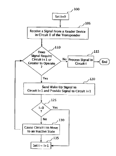
[0030] Figure 7 is a flowchart of a method for managing power consumption in
the
transponder of Figure 6 according to a preferred embodiment of the invention.
DESCRIPTION OF THE PREFERRED EMBODIMENTS
[0031] Figure 1 is a block diagram of an RF transponder 5 according to one
embodiment of the present invention. The RF transponder 5 includes a receiver
10
operatively coupled to an antenna 15. The receiver 10 may be any suitable RF
receiver that is
capable of demodulating an incoming RF signal such as, for example, the
rfRXDO420 UHF
ASK/FSK/FM receiver sold by Microchip Technology Inc. of Chandler Arizona. The
receiver 10 is in electronic communication with a buffer device 20, the
functionality of which
is described in greater detail below. The buffer device 20 is in electronic
communication with
a processing unit 25, which may be, without limitation, a microprocessor, a
microcontroller,
or some other type of processor device. The processing unit 25 may further be
another type
of electronic device, such as a CMOS device or any other electronic circuit
element provided
on, for example, a semiconductor substrate or printed circuit board (PCB),
which performs a
7
CA 02630993 2008-05-23
WO 2007/076191
PCT/US2006/061094
particular function or functions. The processing unit 25 is capable of being
placed into an
inactive, sleep state where the current drawn by it is at a minimum. In
addition, the
processing unit 25 may be woken up, i.e., moved from the inactive, sleep state
to an active
state, upon receipt of an external input signal. An RF transmitter 30, such as
the model
rfPIC12F675F sold by Microchip Technology Inc. of Chandler Arizona, is in
electronic
communication with the processing unit 25. The RF transmitter 30 is, in
response to
commands received from the processing unit 25, able to transmit RF signals
through an
antenna 35 operatively coupled thereto. Like the processing unit 25, the RF
transmitter 30 is
capable of being placed into an inactive, sleep state where the current drawn
by it is at a
minimum, and can be woken up by receipt of an external input signal provided
by the
processing unit 25. The RF transponder 5 also includes a battery 40 which
provides the
power required for the operation of the receiver 10, the buffer device 20, the
processing unit
25 and the transmitter 30. The battery 40 may alternatively be replaced by
another power
source, such as, without limitation, a fuel cell or a so called
supercapacitor.
[0032] The RF transponder 5 is particularly adapted to be utilized in a
transponder
system 50, as shown in Figure 2, wherein a plurality of similarly structured
RF transponders 5
are deployed in a particular location, such as within a building. The
transponder system 50
further includes an interrogator unit 55 which is in electronic communication
with a host
(central) computer system 60. Under the control of the host computer system
60, the
interrogator unit 55 generates the RF signals that are required to selectively
awaken the RF
transponders 5 in the manner described below. In addition, for reasons to be
described below,
each of the RF transponders 5 is assigned at least one identifier, such as a
unique
identification number, that allows the RF transponder 5 to be selectively
identified. That
identifier is stored by the buffer device 20 in each transponder device 5.
Each RF transponder
may, in one embodiment, have a unique identifier that uniquely identifies the
RF
transponder 5 in the system 50. Alternatively or additionally, one or more RF
transponders 5
may share a common identifier so that they may be grouped and identified
together.
[0033] In operation, each of the RF transponders 5, in one embodiment, is
deployed
in a state wherein the receiver 10 and the buffer device 20 thereof are
active, meaning they are
drawing current from the associated battery 40 at a level that allows them to
be fully
functional. In addition, the processing unit 25 and the transmitter 30 of each
RF transponder
5 are, in this embodiment, in the inactive, sleep state. As such, the extent
to which they draw
power from the associated battery 40 will be at a minimum. When it is desired
to "wake-up"
8
CA 02630993 2008-05-23
WO 2007/076191
PCT/US2006/061094
a particular RF transponder 5, such as when it is desired to obtain
information from the RF
transponder 5, an RF information signal of an appropriate frequency that
includes, without
limitation, the particular identifier assigned to the RF transponder 5 of
interest and any
appropriate commands is generated by the interrogator unit 55 and transmitted
to each RF
transponder 5 in the system 50. The information just described may be included
in the RF
information signal by any known technique, such as a known modulation
technique like
frequency shift keying (FSK) or amplitude shift keying (ASK). The RF
information signal is
received by the receiver 10 of each RF transponder 5, where it is demodulated
to obtain a
corresponding information (digital) signal. The information signal, which
includes the
identifier and other information such as one or more commands, is then
provided to the buffer
device 20 of each RF transponder 5.
[0034] The buffer device 20 of each RF transponder 5 receives the information
signal
and compares the identifier identifiers included within the information signal
to the identifier
that is stored in the buffer device 20. In each case, if the buffer device 20
determines that the
received identifier does not match a stored identifier, then no further action
is taken. In the
case or cases where the buffer device 20 of a transponder 5 determines that
the two identifiers
do match, the buffer device 20 generates a DC wake-up signal and provides the
DC wake-up
signal to the sleep input (pin) of the associated processing unit 25. The DC
wake-up signal
causes the processing unit 25 to move from the inactive, sleep state to its
active state. Once
the processing unit 25 has moved to the active state, the buffer device 20
will then provide the
other information, such as one or more commands, based on data included in the
information
signal received from the associated receiver 10 to the processing unit 25. In
the active state,
the processing unit 25 is able to perform any action that is required by the
received
commands, such as waking up the associated RF transmitter 20 and causing it to
transmit an
information signal to the interrogator unit 55. When finished (or after some
predetermined
period of time), the processing unit 25 can return to an inactive, sleep state
until subsequently
woken up as described herein. The buffer device 20 may be any type of device
that includes
electronic circuitry for performing the functionality just described. For
example, the buffer
device 20 may be a PICFXX8 flash microcontroller sold by Microchip Technology
Inc. of
Chandler Arizona or a custom designed electronic circuit, such as a custom
CMOS circuit.
[0035] Thus, as will be appreciated, the system 5 provides improved
performance by
maximizing the life of the batteries 40 included in the RF transponders 5 by
awakening the
9
CA 02630993 2008-05-23
WO 2007/076191
PCT/US2006/061094
processing units 25 of only the one or more RF transponders 5 for which an
information
signal generated by the interrogator unit 55 is intended.
[0036] In an alternative embodiment of the RF transponder 5, the buffer device
20 is
capable of being placed into an inactive, sleep state where the current drawn
by it is at a
minimum, and may be woken up, i.e., moved from the inactive, sleep state to an
active state,
upon receipt of an external input signal. The receiver 10 in this alternative
embodiment of the
RF transponder 5 is adapted to generate a wake-up signal for the buffer device
20 when it
receives a information signal as described above. Thus, in operation, the
buffer device 20 in
this embodiment will remain in a low power sleep state until the information
signal is
received by the receiver 10, at which time it will be awakened to perform the
comparison
described above. As a result, less power will be continuously consumed by the
RF
transponder 5 in this embodiment.
[0037] Figure 3 is a block diagram of an RF transponder 5' according to an
alternative embodiment of the present invention. The RF transponder 5' is
similar in
operation to the RF transponder 5 shown in Figure 1 and may be substituted for
the RF
transponder 5 in the system 50 shown in Figure 2. Like the RF transponder 5,
the RF
transponder 5' includes a receiver 10, an antenna 15, a buffer device 20, a
processing unit 25,
a transmitter 30, an antenna 35 and a battery 40 which function as described
in connection
with Figure 1. The RF transponder 5' differs from the RF transponder 5,
however, in that
instead of having a buffer device 20 that is operatively coupled to and
continuously powered
by the battery 40, the buffer device 20 receives operational power from an
energy harvesting
circuit 65 that harvests energy that is transmitted in space. As employed
herein, the term "in
space" means that energy or signals are being transmitted through the air or
similar medium
regardless of whether the transmission is within or partially within an
enclosure, as contrasted
with transmission of electrical energy by a hard wired or printed circuit
boards. A number of
methods and apparatus for harvesting energy from space and using the harvested
energy to
power an electronic device are described in United States Patent No.
6,289,237, entitled
"Apparatus for Energizing a Remote Station and Related Method," United States
Patent No.
6,615,074, entitled "Apparatus for Energizing a Remote Station and Related
Method," United
States Patent No. 6,856,291, entitled "Energy Harvesting Circuits and
Associated Methods,"
and United States Patent Application Publication No. 2005/0030181, entitled
"Antenna on a
Wireless Untethered Device such as a Chip or Printed Circuit Board for
Harvesting Energy
CA 02630993 2013-01-11
71548-302
from Space", each assigned to the assignee hereof.
[0038] The preferred energy harvesting circuit 65 is shown in Figure 4 and
includes
an antenna 70, which may be, without limitation, a square spiral antenna. The
antenna 70 is
electrically connected to a matching network 75, which in turn is electrically
connected to a
voltage boosting and rectifying circuit in the form of a charge pump 80.
Charge pumps are
well known in the art. Basically, one stage of a charge pump essentially
doubles the effective
= amplitude of an AC input voltage and-stores the resulting increased DC
voltage on an output
capacitor. The voltage could also be stored using a rechargeable battery.
Successive stages of
a charge pump, if present, will essentially increase the voltage from the
previous stage
resulting in an increased output voltage. In operation, the antenna 70
receives energy, such as
RF energy, that is transmitted in space by a far-field source, such as an RF
source. The RF
source may be, for example, the interrogator unit 55, in which case the RF
energy may be the
information signal transmitted by the interrogator unit 55, or a local radio
station, in which
case the RF energy comprises ambient RF energy in the vicinity of the RF
transponder 5'.
The RF energy received by the antenna 70 is provided, in the form of an AC
signal, to the
charge pump 80 through the matching network 75. The charge pump 80 amplifies
and
rectifies the received AC signal to produce a DC signal. The matching network
75 preferably
matches the impedance of the charge pump 80 to the impedance of the antenna 70
in a manner
= that optimizes the amount of energy that is harvested (i.e., maximum DC
output). In one
particular embodiment, the matching network 75 is an LC tank circuit formed by
the inherent
distributed inductance and inherent distributed capacitance of the conducing
elements of the
antenna 70. Such an LC tank circuit has a non-zero resistance R which results
in the
retransmission of some of the incident RF energy. This retransmission of
energy may cause
the effective area of the antenna 70 to be greater than the physical area of
the antenna 70. The
DC signal generated by the charge pump 80 is provided to the buffer device 20
provided in
the RF transponder 5' for powering the buffer device 20. Thus, the buffer
device 20 in the RF
transponder 5' is able to be powered remotely without the need, as in the case
of the RF
-transponder 5, to continuously consume power from the battery 40. As will be
appreciated,
this is advantageous in that it further extends the life of the RF transponder
5' by finther
minimizing consumption of power from the battery 40.
[00391 Figure 5 is a block diagram of an RF transponder 5" according to a
further
alternative embodiment of the present invention. The RF transponder 5" is
similar in
11
CA 02630993 2008-05-23
WO 2007/076191
PCT/US2006/061094
operation to the RF transponder 5 shown in Figure 1 and the RF transponder 5'
shown in
Figure 3 and may be substituted for the RF transponder 5 or the RF transponder
5' in the
system 50 shown in Figure 2. Like the RF transponder 5, the RF transponder 5"
includes an
antenna 15, a processing unit 25, a transmitter 30, an antenna 35 and a
battery 40 which
function as described in connection with Figure 1. The RF transponder 5"
differs from the RF
transponder 5 in that instead of having a receiver 10 and a buffer device 20
that are
operatively coupled to and continuously powered by the battery 40, it includes
a combination
receiver/buffer device 20' that combines the functionality of the receiver 10
and the buffer
device 20 described elsewhere herein in a single device. The receiver/buffer
device 20'
receives operational power from an energy harvesting circuit 65 that harvests
energy that is
transmitted in space. As will be appreciated, this configuration is
advantageous in that it still
further extends the life of the RF transponder 5" by even further minimizing
the consumption
of power from the battery 40.
100401 Figure 6 is a schematic representation of a transponder 70 according to
another embodiment of the present invention. The transponder 70 includes n
circuits 75
(labeled circuit 0 through circuit n-1 in Figure 6), each of which is
connected to a source of
power, such as a single power supply 80 (e.g., a battery, fuel cell or
supercapacitor) as shown
in Figure 6, or alternatively, any one of multiple power supplies provided as
part of
transponder 70. Each circuit 75 may be, without limitation, an integrated
circuit chip or other
electronic device. For example, and without limitation, each circuit 75 may an
RF receiver,
an RF transmitter, a 30 KHz tone circuit, a buffer device (as described
elsewhere herein), a
custom integrated circuit (e.g., a custom CMOS circuit), or a processing unit
such as a
microprocessor or microcontroller, among other devices. In addition, each
circuit 75 has a
power requirement p(i) which represents the power that is required/consumed
during
operation of the particular circuit 75. In the transponder 70, p(0) < p(1) <
p(2) < ...< p(n-1),
or put another way, p(i-1) < p(i). As such, the nth circuit 75 (labeled
circuit n-1), which may
be, for example, a processing unit, has the highest power requirement and the
1st circuit 75
(labeled circuit 0) has the lowest power requirement. Also, as seen in Figure
6, the circuits 75
are connected to one another in a sequence that corresponds to their
respective power levels,
meaning that circuit 0 is connected to circuit 1, circuit 1 is connected to
circuit 2, and so on.
Furthermore, each circuit 75 may be provided on a separate substrate or die,
or, alternatively,
one or more (or all) of the circuits 75 may be provided on the same (common)
substrate or
die. Finally, at least each of the circuits 75 after circuit 0 in the sequence
is capable of being
12
CA 02630993 2008-05-23
WO 2007/076191
PCT/US2006/061094
placed into an inactive, sleep state where the current drawn by it is at a
minimum, and is able
to be woken up, i.e., moved from the inactive, sleep state to an active state,
upon receipt of an
input signal (a wake-up signal). Preferably, the 1st circuit 75 (labeled
circuit 0) remains in an
active state at all times to be able to receive incoming signals from a reader
device, such as
the interrogator unit 55 shown in Figure 2, although it is possible for the
1st circuit 75 (labeled
circuit 0) to also be capable of moving from an inactive, sleep state to an
active state upon
receipt of an input (wake-up) signal.
[0041] According to this embodiment of the invention, the objective is to
awaken
each circuit 75 in the sequence 0, 1, 2, ..., n-1 only as necessary. In
particular, in response to
receiving a inquiry signal from a reader device, such as the interrogator unit
55 shown in
Figure 2, a wake up signal is only given to the next highest circuit 75 if it
is determined by the
current circuit 75 that the inquiry signal may be intended for/require the
operation of the next
circuit 75 or greater in the sequence. Thus, through this sequence of
increasing power circuits
75, only that power that is necessary is actually consumed (as opposed to
unnecessarily
awakening higher power circuits 75 which are not required for processing the
inquiry signal).
Also, as the itit circuit 75 in the sequence is awakened, the ith-1 circuit 75
in the sequence may
be caused to move back to an inactive state, such as in response to the logic
of the circuit or in
response to a command received from the reader device as part of a protocol.
As a result, the
transponder 70, including the circuits 75, implements a power optimized ladder
architecture.
[0042] Figure 7 is a flowchart of a method for managing power consumption in
the
transponder 70 (based on the power optimized ladder architecture described
above) according
to a preferred embodiment of the invention. The method begins at step 100,
wherein a
counter I is et to zero. Next, at step 105, a signal from a reader device,
such as the
interrogator unit 55 shown in Figure 2, is received in the circuit 75 labeled
as circuit 0 (this
circuit 75 may be, for example, an RF transmitter or a 30 KHz tone receiving
circuit). Next,
at step 110, the circuit 75 labeled as circuit i (which initially is circuit
0) makes a
determination, based on information included in the received signal, as to
whether the
received signal requires the circuit 75 labeled as circuit i+1 or higher to
operate (i.e., process
the signal). If the answer at step 110 is no, then, at step 115, the received
signal is processed
in the circuit 75 labeled as circuit i. If, however, the answer at step 110 is
yes, then, at step
120, the circuit 75 labeled as circuit i sends a wake-up signal to the circuit
75 labeled as
circuit i+1 and provides the received signal to the circuit 75 labeled as
circuit i+1. Next, at
step 125, a determination is made as to whether the counter i equals zero. If
the answer at
13
CA 02630993 2013-01-11
71548-302
step 125 is no, then, at step 130, the circuit 75 labeled as circuit i is
caused to move to an
inactive state. Then, at step 135, the counter i is set equal to i+1. If,
however, the answer at
step 125 is yes, then the method proceeds directly to step 135. Following step
135, the
method returns to step 110 for further processing as described herein.
[0043] While preferred embodiments of the invention have been described and
illustrated above, it should be understood that these are exemplary of the
invention and are not
to be considered as limiting. Additions, deletions, substitutions, and other
modifications can
be made without departing from the scope of the present invention.
Accordingly, the
invention is not to be considered as limited by the foregoing description but
is only limited by
the scope of the appended claims.
=
14